 | –≠–ª–µ–∫—Ç—Ä–æ–Ω–Ω—ã–π –∫–æ–º–ø–æ–Ω–µ–Ω—Ç: MSA-0786 | –°–∫–∞—á–∞—Ç—å:  PDF PDF  ZIP ZIP |
Document Outline
- List of Figures
- 1. Typical Power Gain vs. Frequency
- 2. Device Current vs. Voltage
- 3. Output Power at 1 dB Gain Compression, NF and Power Gain vs. Case Temperature
- 4. Output Power at 1 dB Gain Compression vs. Frequency
- 5. Noise Figure vs. Frequency
- Features
- Typical Biasing Configuration
- Description
- 86 Plastic Package
- MSA-0786 Absolute Maximum Ratings
- Electrical Specifications
- Part Number Ordering Information
- MSA-0786 Typical Scattering Parameters
- Typical Performance
- 86 Plastic Package Dimensions
6-406
Cascadable Silicon Bipolar
MMIC Amplifier
Technical Data
Features
∑ Cascadable 50
Gain Block
∑ Low Operating Voltage:
4.0 V Typical V
d
∑ 3 dB Bandwidth:
DC to 2.0 GHz
∑ 12.5 dB Typical Gain at
1.0 GHz
∑ Unconditionally Stable
(k>1)
∑ Surface Mount Plastic
Package
∑ Tape-and-Reel Packaging
Option Available
[1]
MSA-0786
86 Plastic Package
Description
The MSA-0786 is a high perfor-
mance silicon bipolar Monolithic
Microwave Integrated Circuit
(MMIC) housed in a low cost,
surface mount plastic package.
This MMIC is designed for use as a
general purpose 50
gain block.
Applications include narrow and
broad band IF and RF amplifiers
in commercial and industrial
applications.
The MSA-series is fabricated using
HP's 10 GHz f
T
, 25 GHz f
MAX
,
silicon bipolar MMIC process
which uses nitride self-alignment,
ion implantation, and gold metalli-
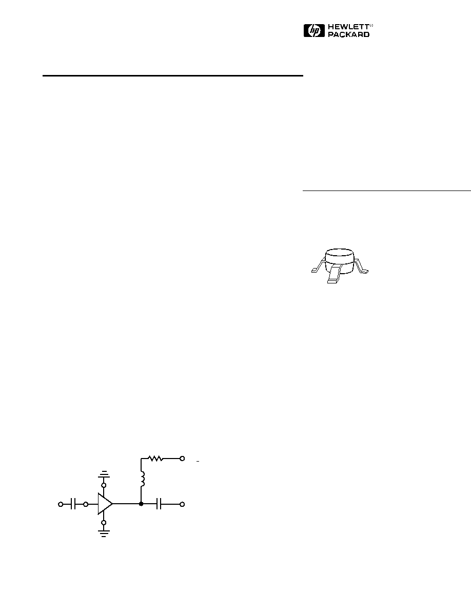
Typical Biasing Configuration
C
block
C
block
R
bias
V
CC
>
5 V
V
d
= 4.0 V
RFC (Optional)
IN
OUT
MSA
4
1
2
3
Note:
1. Refer to PACKAGING section "Tape-
and-Reel Packaging for Semiconduc-
tor Devices."
zation to achieve excellent
performance, uniformity and
reliability. The use of an external
bias resistor for temperature and
current stability also allows bias
flexibility.
5965-9594E

6-407
MSA-0786 Absolute Maximum Ratings
Parameter
Absolute Maximum
[1]
Device Current
60 mA
Power Dissipation
[2,3]
275 mW
RF Input Power
+13 dBm
Junction Temperature
150
∞
C
Storage Temperature
≠65 to 150
∞
C
Thermal Resistance
[2,4]
:
jc
= 120
∞
C/W
Notes:
1. Permanent damage may occur if any of these limits are exceeded.
2. T
CASE
= 25
∞
C.
3. Derate at 8.3 mW/
∞
C for T
C
> 117
∞
C.
4. See MEASUREMENTS section "Thermal Resistance" for more information.
Part Number Ordering Information
Part Number
No. of Devices
Container
MSA-0786-TR1
1000
7" Reel
MSA-0786-BLK
100
Antistatic Bag
For more information, see "Tape and Reel Packaging for Semiconductor Devices".
G
P
Power Gain (|S
21
|
2
)
f = 0.1 GHz
dB
13.5
f = 1.0 GHz
10.5
12.5
G
P
Gain Flatness
f = 0.1 to 1.3 GHz
dB
±
0.7
f
3 dB
3 dB Bandwidth
GHz
2.0
Input VSWR
f = 0.1 to 2.5 GHz
1.7:1
Output VSWR
f = 0.1 to 2.5 GHz
1.7:1
NF
50
Noise Figure
f = 1.0 GHz
dB
5.0
P
1 dB
Output Power at 1 dB Gain Compression
f = 1.0 GHz
dBm
2.0
IP
3
Third Order Intercept Point
f = 1.0 GHz
dBm
19.0
t
D
Group Delay
f = 1.0 GHz
psec
150
V
d
Device Voltage
V
3.2
4.0
4.8
dV/dT
Device Voltage Temperature Coefficient
mV/
∞
C
≠7.0
Note:
1. The recommended operating current range for this device is 15 to 40 mA. Typical performance as a function of current
is on the following page.
Electrical Specifications
[1]
, T
A
= 25
∞
C
Symbol
Parameters and Test Conditions: I
d
= 22 mA, Z
O
= 50
Units
Min.
Typ.
Max.
VSWR

6-408
MSA-0786 Typical Scattering Parameters (Z
O
= 50
, T
A
= 25
∞
C, I
d
= 22 mA)
Freq.
GHz
Mag
Ang
dB
Mag
Ang
dB
Mag
Ang
Mag
Ang
0.1
.05
175
13.5
4.74
174
≠18.7
.116
1
.14
≠12
0.2
.05
174
13.4
4.71
169
≠18.7
.117
3
.14
≠22
0.4
.04
167
13.3
4.64
158
≠18.4
.120
4
.15
≠44
0.6
.04
175
13.1
4.52
148
≠18.3
.122
7
.16
≠65
0.8
.05
≠156
12.9
4.39
138
≠18.0
.126
8
.17
≠84
1.0
.06
≠134
12.6
4.25
127
≠17.5
.134
10
.18
≠102
1.5
.08
≠142
11.6
3.79
103
≠16.6
.148
9
.21
≠139
2.0
.15
≠159
10.5
3.34
80
≠15.7
.164
7
.23
≠164
2.5
.25
≠176
9.2
2.89
63
≠15.1
.176
5
.24
174
3.0
.33
166
7.8
2.45
44
≠14.7
.185
1
.24
159
3.5
.41
150
6.5
2.11
27
≠14.9
.179
≠5
.24
149
4.0
.49
137
5.2
1.82
12
≠15.1
.177
≠9
.23
145
5.0
.60
116
3.0
1.41
≠14
≠15.4
.169
≠14
.26
145
Note:
1. A model for this device is available in the DEVICE MODELS section.
S
11
S
21
S
12
S
22
G
p
(dB)
0.1
0.3 0.5
1.0
3.0
6.0
FREQUENCY (GHz)
Figure 1. Typical Power Gain vs.
Frequency.
1
0
2
3
4
5
V
d
(V)
Figure 2. Device Current vs. Voltage.
0
2
4
6
8
10
12
16
14
0
10
20
30
40
Gain Flat to DC
I
d
(mA)
T
C
= +85
∞
C
T
C
= +25
∞
C
T
C
= ≠25
∞
C
0.1
0.2 0.3
0.5
2.0
1.0
4.0
FREQUENCY (GHz)
Figure 4. Output Power at 1 dB Gain
Compression vs. Frequency.
≠3
0
3
6
15
12
9
P
1 dB
(dBm)
I
d
= 22 mA
I
d
= 40 mA
I
d
= 15 mA
I
d
= 22 mA
I
d
= 40 mA
I
d
= 15 mA
5.0
4.5
5.5
6.0
6.5
NF (dB)
FREQUENCY (GHz)
Figure 5. Noise Figure vs. Frequency.
0.1
0.2 0.3
0.5
2.0
1.0
4.0
4
5
6
4
5
6
12
13
14
≠25
+25
0
+55
+85
P
1 dB
(dBm)
NF (dB)
Gp (dB)
TEMPERATURE (
∞
C)
Figure 3. Output Power at 1 dB Gain
Compression, NF and Power Gain vs.
Case Temperature, f = 1.0 GHz,
I
d
=22mA.
NF
P
1 dB
G
P
I
d
= 15 mA
I
d
= 22 mA
I
d
= 40 mA
Typical Performance, T
A
= 25
∞
C
(unless otherwise noted)
6-409
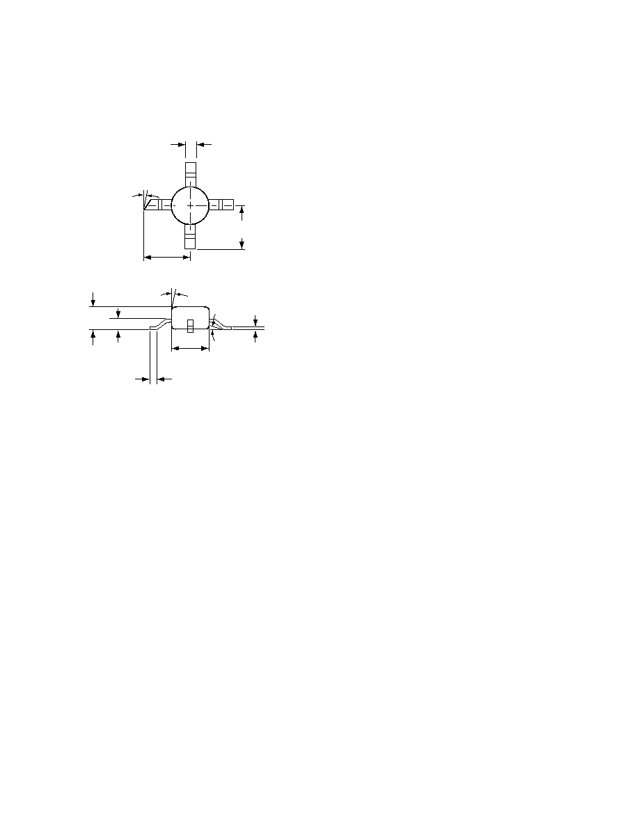
86 Plastic Package Dimensions
4
0.51
±
0.13
(0.020
±
0.005)
2.34
±
0.38
(0.092
±
0.015)
2.67
±
0.38
(0.105
±
0.15)
1
3
2
2.16
±
0.13
(0.085
±
0.005)
DIMENSIONS ARE IN MILLIMETERS (INCHES)
1.52
±
0.25
(0.060
±
0.010)
0.66
±
0.013
(0.026
±
0.005)
0.203
±
0.051
(0.006
±
0.002)
0.30 MIN
(0.012 MIN)
C
L
45
∞
5
∞
TYP.
8
∞
MAX
0
∞
MIN
GROUND
RF INPUT
RF OUTPUT
AND DC BIAS
GROUND
A07