AIC1570
5-bit DAC, Synchronous PWM Power Regulator
with LDO and Linear Controller
Analog Integrations Corporation
4F, 9 Industry E. 9th Rd, Science-Based Industrial Park, Hsinchu, Taiwan
DS-1570-01 012102
TEL: 886-3-5772500
FAX: 886-3-5772510
www.analog.com.tw
1
n
FEATURES
l
Compatible with HIP6018.
l
Provides 3 Regulated Voltages for Micro-
processor Core, Clock and GTL Power.
l
Simple Voltage-Mode PWM Control.
l
Dual N-Channel MOSFET Synchronous Driver.
l
Operates from +3.3V, +5V and +12V Inputs.
l
Fast Transient Response.
l
Full 0% to 100% Duty Ratios.
l
±1.0% Output Voltage for VCORE and
±
2.0%
Output Voltage Reference for VCLK and VGTL.
l
TTL Compatible 5-bit Digital-to-Analog Core
Output Voltage Selection. Range from 1.3V to
3.5V.
0.1V Steps from 2.1V to 3.5V.
0.05V Steps from 1.3V to 2.05V.
l
Adjustable Current Limit without External Sense
Resistor.
l
Microprocessor Core Voltage Protection against
Shorted MOSFET.
l
Power Good Output Voltage Monitor.
l
Over-Voltage and Over-Current Fault Monitors.
l
200KHz Free-Running Oscillator Programmable
up to 350KHz.
n
APPLICATIONS
l
Full Motherboard Power Regulation for
Computers.
n
DESCRIPTION
The AIC1570 combines a synchronous voltage
mode controller with a low dropout linear regulator
and a linear controller as well as the monitoring and
protection functions in this chip. The PWM
controller regulates the microprocessor core
voltage with a synchronous rectified buck converter.
The linear controller regulates power for the GTL
bus and the linear regulator provides power for the
clock driver circuit.
An integrated 5 bit D/A converter that adjusts the
core PWM output voltage from 2.1V to 3.5V in 0.1V
increments and from 1.3V to 2.05V in 0.05V
increments. The linear regulator uses an internal
driver device to provide 2.5V±2.5%. The linear
controller drives with an external N-channel
MOSEFET to provide 1.5V±2.5%.
This chip monitors all the output voltages. Power
Good signal is issued when the core voltage is
within ±10% of the DAC setting and the other levels
are above their under-voltage levels. Over-voltage
protection for the core output uses the lower N-
channel MOSFET to prevent output voltage above
115% of the DAC setting.
The PWM over-current function monitors the output
current by using the voltage drop across the upper
MOSFET's R
DS(ON)
, eliminating the need for a
current sensing resistor.

AIC1570
3
n
ORDERING INFORMATION
PACKING TYPE
TR: TAPE & REEL
TB: TUBE
PACKAGING TYPE
S: SMALL OUTLINE
AIC1570 CXX X
Example: AIC1570CSTR
ý
in SO-24 Package & Taping & Reel
Packing Type
PIN CONFIGURATION
1
3
4
2
5
7
6
8
9
10
11
12
VID0
VID4
VID3
VID2
VCC
VID1
RT
PGOOD
S S
FAULT
VIN2
FB2
16
15
24
22
23
21
20
19
17
18
14
13
LGATE
UGATE
PHASE
VSEN
P GND
OCSET
FB1
GATE3
COMP1
FB3
VOUT2
GND
SO-24
TOP VIEW
n
ABSOLUTE MAXIMUM RATINGS
Supply Voltage, V
CC
.................. ... ... ... ... ........ ... ... ... ............ ..... ... ..................... +15V
PGOOD, FAULT and GATE Voltage
........ ... ........ ... ... ..... .... GND -0.3V to V
CC
+0.3V
Input, Output , or I/O Voltage ......... ...... ... ... ... ... ... ... ... ..... ... ............ GND -0.3V to 7V
Recommended Operating Conditions
Supply Voltage; VCC
... ... .................. ................... +12V±10%
Ambient temperature Range
... ... ..... ... ... ... ... ................. 0
∞
C~70
∞
C
Maximum Operation Junction Temperature ... ... ......... ... ... ..... 100
∞
C
Thermal Information
Thermal Resistance,
JA
SOIC package
... ... ... ... ... ... ... ... ... ... ... ... ... ..... ............... 100
∞
C/W
SOIC package (with 3in
2
of copper)
... ...... ... ... .......... ......... 90
∞
C/W
Maximum Junction Temperature (Plastic Package)
... ... ... ... ... ... ..... ... ...... 150
∞
C
Maximum Storage Temperature Range ... ... ... ... ... ... ... ... ... ... ... .... -65
∞
C ~ 150
∞
C
Maximum Lead Temperature (Soldering 10 sec)
... ... ... ... ... ... ... ... ... ..... ... 300
∞
C
n
TEST CIRCUIT
Refer to TYPICAL APPLICATION CIRCUIT.
AIC1570
4
n
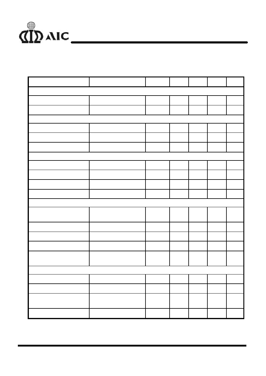
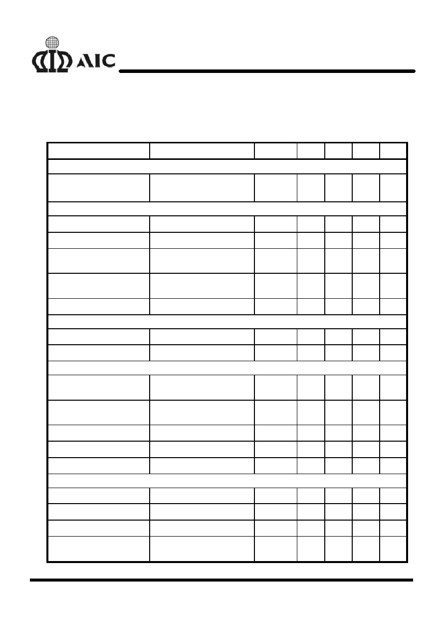
ELECTRICAL CHARACTERISTICS
(V
cc
=12V, T
A
=25
∞
C, Unless otherwise
specified)
PARAMETER
TEST CONDITIONS
SYMBOL
MIN.
TYP.
MAX.
UNIT
VCC SUPPLY CURRENT
Supply Current
UGATE, LGATE, GATE3 and
VOUT2 open
I
CC
1.8
5
mA
POWER ON RESET
Rising VCC Threshold
V
OCSET
=4.5V
VCC
THR
8.6
9.5
10.4
V
Falling VCC Threshold
V
OCSET
=4.5V
VCC
THF
8.2
9.2
10.2
V
Rising VIN2 Under-Voltage
Threshold
VIN2
THR
2.5
2.6
2.7
V
VIN2 Under-Voltage
Hysteresis
VIN2
HYS
130
mV
Rising V
OCSET1
Threshold
V
OCSETH
1.3
V
OSCILLATOR
Free Running Frequency
RT=Open
F
170
200
230
KHz
Ramp. Amplitude
RT=open
V
OSC
1.3
V
P-P
REFERENCE AND DAC
DAC (VID0~VID4) Input Low
Voltage
VID
L
0.8
V
DAC (VID0~VID4) Input
High Voltage
VID
H
2
V
DACOUT Voltage Accuracy
VDAC=1.8V~3.5V
-1.0
+1.0
%
FB2 Reference Voltage
V
REF2
1.240
1.265
1.290
V
FB3 Reference Voltage
V
REF3
1.250
1.275
1.300
V
LINEAR REGULATOR
Regulation
10mA<I
OUT2
<150mA
-1
+1
%
Under-Voltage Level
FB2 falling
FB2
UV
70
82
%
Over-Current Protection
430
570
mA
Over-Current Protection
During Start-up
750
mA