AIC1580/L
Simple PWM Power Regulator with Shutdown
Analog Integrations Corporation
4F, 9, Industry E. 9th Rd, Science Based Industrial Park, Hsinchu Taiwan, ROC
www.analog.com.tw
DS-1580-00 Sep 5, 00
TEL: 886-3-5772500
FAX: 886-3-5772510
1
FEATURES
Operation Voltage up to 15V.
Simple Voltage-Mode PWM Control.
Fast Transient Response.
2V and 1.3V
± 2% Feedback Voltage Reference
Option.
Adjustable Current Limit without External Sense
Resistors.
200KHz Free-Running Oscillator.
Short-Circuit Protection with Low Short Circuit
Output Current.
Low Shutdown Current
Built-in Soft Start.
APPLICATIONS
Power Supply for Motherboard V
GTL
(1.5V Output)
Power Supply for Motherboard V
I/O
.
High-Power 5V to 3.xV DC/DC Regulators.
Low-Voltage Distributed Power Supplies.
DESCRIPTION
The AIC1580 is a high-power, high-efficiency
voltage-mode switching regulator controller for
motherboard V
I/O
power supply applications.
Designed to drive a N-channel MOSFET in a
standard buck topology, the AIC1580 features a
high voltage CMOS output driver, short-circuit
protection, and 8-pin package.
An external 4-bit Digital-to-Analog Converter
(DAC) can be used along with the AIC1580 to
adjust the output voltage from 2.0V to 3.5V in
0.1V increments. Table 1 on the following page
specifies the corresponding output voltage for
16 combinations of DAC inputs as in the typical
application circuit.
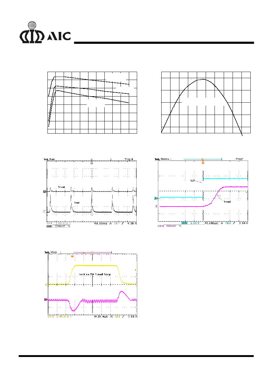
The 200KHz switching frequency allows for
using small external components while
maintaining high conversion efficiency. The
11MHz bandwidth and 6V/
µS slew rate of the
error amplifier ensures high converter
bandwidth and fast transient response.
The AIC1580 provides adjustable overcurrent
and short-circuit protections by sensing the
output current across the on resistance of the
external N-channel MOSFET rather than an
external low value sense resistor.
The AIC1580L provides lower reference voltage
(1.30V) than the default (2.00V, AIC1580) for
lower V
OUT
requirement.
AIC1580/L
2
ORDERING INFORMATION
ORDER NUMBER
AIC1580CN
AIC1580LCN
(PLASTIC DIP)
AIC1580CS
AIC1580LCS
(PLASTIC SO)
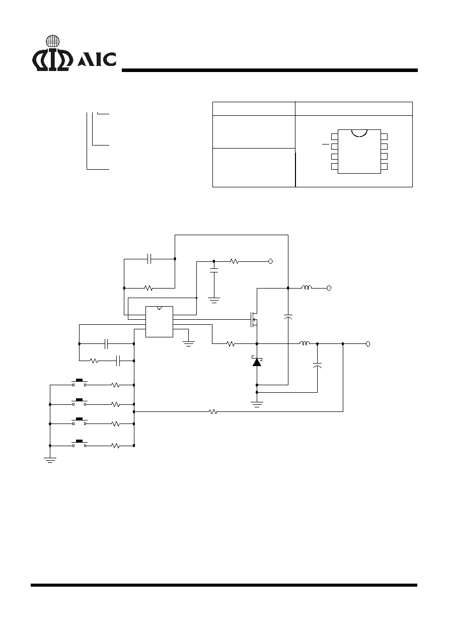
PIN CONFIGURATION
TOP VIEW
PHASE
1
3
4
2
VCC
SD
COMP
FB*
UGATE
GND
8
6
5
7
OCSET
PACKAGE TYPE
N: PLASTIC DIP
S: SMALL OUTLINE
TEMPERATURE RANGE
C=0
∞C~+70∞C
REFERENCE VOLTAGE
DEFAULT: 2.00V
L: 1.30V
AIC1580 XXX
*AIC1580: 2.00V
AIC1580L: 1.30V
TYPICAL APPLICATION CIRCUIT
VID2
VID1
VID0
VID3
AIC1580
FB
GND
PHASE
SD
VCC
CLSET
COMP
UDRI
C1
1U
C7
33P C6
1000P
C9
1000P
+
C4
6000UF
+
C3
3000UF
R5
3.01K
R9
5K
R4
15.0K
R8
30.1K
R7
6.04K
R6
90.9K
R3
7.5K
R1
10
R2
2.2K
L2
7U
L1
1.5U
D1
SRA1620
M1
IR3303
*C1 MUST BE VERY CLOSE TO VCC PIN
VOUT
5V
12V
Switching Regulator for Pentium
V
CORE
Supply

AIC1580/L
3
Table 1. Output Voltage Program
VID3
VID2
VID1
VID0
VOUT
1
1
1
1
2.00V
1
1
1
0
2.10V
1
1
0
1
2.20V
1
1
0
0
2.30V
1
0
1
1
2.40V
1
0
1
0
2.50V
1
0
0
1
2.60V
1
0
0
0
2.70V
0
1
1
1
2.80V
0
1
1
0
2.90V
0
1
0
1
3.00V
0
1
0
0
3.10V
0
0
1
1
3.20V
0
0
1
0
3.30V
0
0
0
1
3.40V
0
0
0
0
3.50V
ABSOLUTE MAXIMUM RATINGS
Supply Voltage, V
CC
.................................................................................................... 15V
Input, Output, or I/O Voltage .................................................... GND - 0.3V to VCC+0.3V
ESD Classification ................................................................................................. Class 2
Recommended Operating Conditions
Supply Voltage, V
CC
........................................................................................... 12V
±10%
Ambient Temperature Range ............................................................................ 0
∞C~70∞C
Junction Temperature Range ......................................................................... 0
∞C~ 100∞C
Thermal Information
Thermal Resistance,
JA
(Typical, Note 1)
SOIC Package ....................................................................................... 100
∞C/W
SOIC Package (with 3 in
2
of Copper) ..................................................... 90
∞C/W
Maximum Junction Temperature (Plastic Package) .............................................. 150
∞C
Maximum Storage Temperature Range ................................................... ≠65
∞C~150∞C
Maximum Lead Temperature (Soldering 10 Sec) ................................................ 300
∞C
Note 1:
JA
is measured with the component mounted on an evaluation PC board in free air.
TEST CIRCUIT
Refer to TYPICAL APPLICATION CIRCUIT.