 | –≠–ª–µ–∫—Ç—Ä–æ–Ω–Ω—ã–π –∫–æ–º–ø–æ–Ω–µ–Ω—Ç: AIC1628 | –°–∫–∞—á–∞—Ç—å:  PDF PDF  ZIP ZIP |

AIC1628
3-Cell, High-Efficiency, Step-Up DC/DC Converter
Analog Integrations Corporation
4F, 9, Industry E. 9th Rd, Science Based Industrial Park, Hsinchu Taiwan, ROC
www.analog.com.tw
DS-1628-00
TEL: 886-3-5772500
FAX: 886-3-5772510
1
FEATURES
4V to 24V Input Voltage Operation.
Adjustable Output Voltage.
Low Quiescent Current at 100
µA.
Pulse-Skipping and Pulse-Frequency Modulation
Maintain High Efficiency (max. 95%).
90KHz to 250KHz Oscillator Frequency.
Power-Saving Shutdown Mode (8
µA Typical).
Push-Pull Driver Output.
APPLICATIONS
Flash Memory Programming Power Supply.
Positive LCD Contrast Bias for Notebook &
Palmtop Computers.
Step-Up DC/DC Converter Module.
Telecom Power Supply.
DESCRIPTION
The AIC1628 is a high performance step-up
DC/DC converter, designed to drive an external
power switch to generate programmable posi-
tive voltages. In the particularly suitable LCD
contrast bias and flash memory programming
power supply applications, typical full-load effi-
ciencies are 85% to 95%. 4V to 24V input op-
eration range allows the AIC1628 to be powered
directly by the battery pack in the most battery-
operated applications for greater efficiency.
Output voltage can be scaled to 40V or greater
by two external resistors. A Pulse-Frequency
Modulation scheme is employed to maintain
high efficiency conversion under wide input
voltage range. Quiescent current is about
100
µA and can be reduced to 8µA in shutdown
mode. Switching frequency being around 90KHz
to 250KHz range, small size switching compo-
nents are ideal for battery powered portable
equipments, like notebook and palmtop com-
puters.
TYPICAL APPLICATION CIRCUIT
AIC1628
CL
DHI
DLOW
FB
GND
SHDN
VIN
VREF
+36V
>50mA
V
OUT
1N5819
C5
+
C6
V
IN
+5V ~ 24V
C1
120
µF
+
5V
*Buss Fuse MCR-2A
**Sumida CDR105
*Fuse
60m
68
µH
0.047
µ
F
C2
R1
470K
R2
16.5K 0.033µF
C3
220
µF
0.1
µF
D1
2SK940
0.01
µF
C4
**L1
Q1
Load Current (mA)
Ef
f
i
ci
e
n
c
y
(
%
)
V
IN
=13V
0
50
100
150
200
80
85
90
95
V
IN
=18V
V
IN
=9V
V
IN
=5V
V
OUT
=36V
Color LCD Contrast Bias Supply
Efficiency vs. Output Current
AIC1628
2
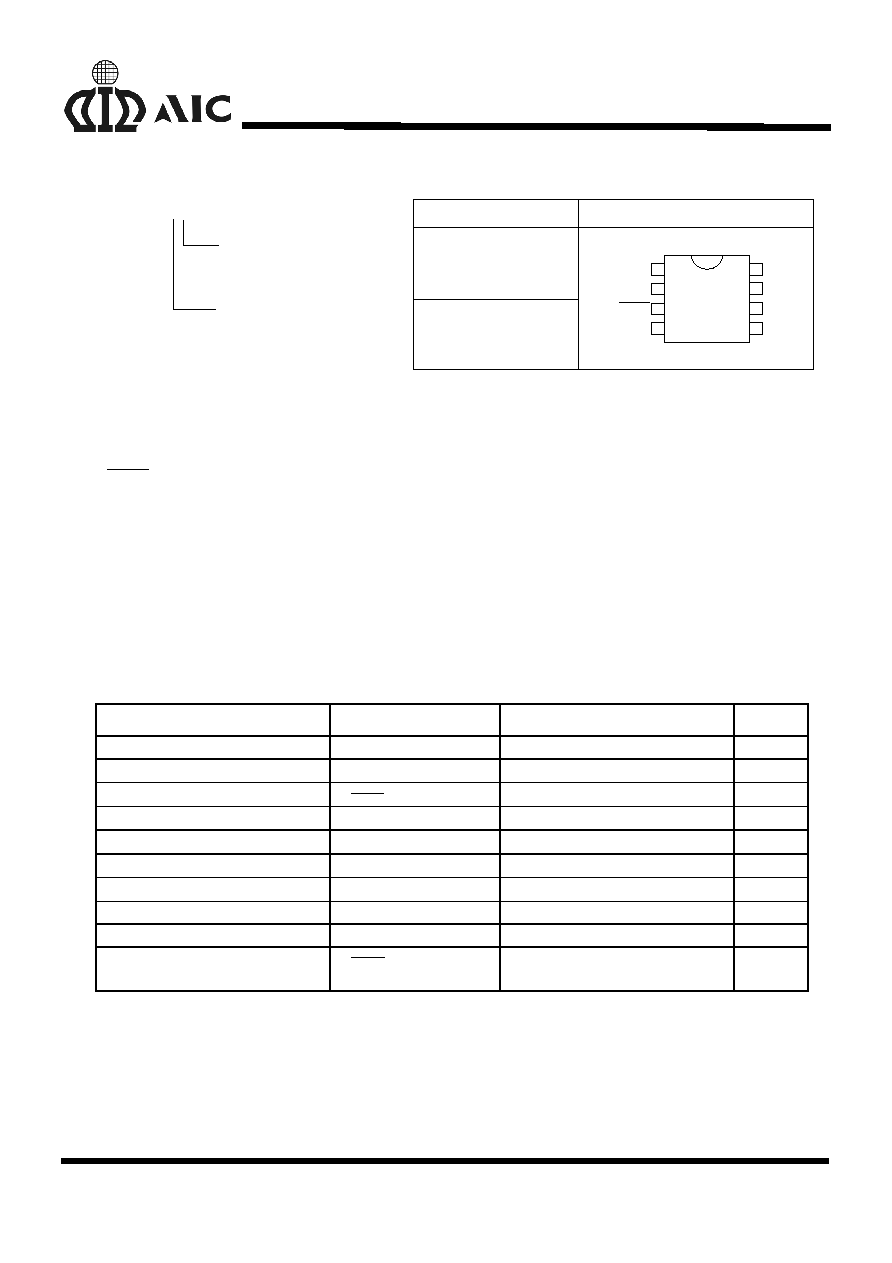
ORDERING INFORMATION
AIC1628 XX
PACKAGE TYPE
N: PLASTIC DIP
S: SMALL OUTLINE
TEMPERATURE RANGE
C=0
∞C~+70∞C
ORDER NUMBER
AIC1628CN
(PLASTIC DIP
)
PIN CONFIGURATION
AIC1628CS
(PLASTIC SO)
TOP VIEW
DLOW
1
3
4
2
8
6
5
7
CL
VREF
SHDN
FB
DHI
GND
VIN
ABSOLUTE MAXIMUM RATINGS
VIN Supply Voltage (V
IN
Pin)
........................................................................................
24V
SHDN Pin Voltage
........................................................................................................
15V
Operating Temperature Range
............................................................................
0
∞C~70∞C
Storage Temperature Range
........................................................................
-65
∞C~ 150∞C
TEST CIRCUIT
Refer to Typical Application Circuit
ELECTRICAL CHARACTERISTICS
(V
IN
= 13V, Ta=25
∞
∞
∞
∞C, unless otherwise
specified.)
PARAMETERS
TEST CONDITIONS
MIN.
TYP.
MAX.
UNIT
Input Voltage
4
24
V
Quiescent Current
V
FB
= 1.5V
100
200
µA
Shutdown Mode Current
V
SHDN
= 0V
8
20
µA
V
REF
Voltage
I
SOURCE
= 250
µA
1.16
1.22
1.28
V
V
REF
Source Current
250
µA
DLOW "ON Resistance"
15
DHI "ON Resistance"
10
CL Threshold
V
IN
- V
CL
45
60
75
mV
Shutdown Threshold
0.8
1.5
2.4
V
Shutdown Input Leakage
Current
V
SHDN
< 15V
1
µA
AIC1628
3
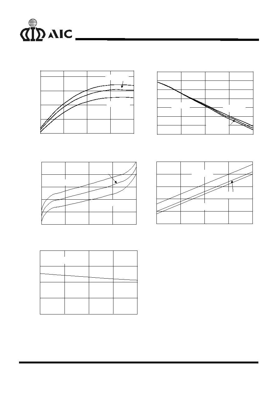
TYPICAL PERFORMANCE CHARACTERISTICS
Frequency vs V
IN
Voltage
V
IN
(V)
4
9
14
19
24
80
130
180
230
280
Ta= 0
∞C
Ta= 25
∞C
Ta= 70
∞C
Fr
equenc
y
(
K
Hz)
Duty Cycle vs V
IN
Voltage
100
V
IN
(V)
30
40
50
60
70
80
90
4
9
14
19
24
Ta= 70
∞C
Ta= 25
∞C
Duty
Cy
cle (
%
)
Ta= 0
∞C
Quiescent Current vs V
IN
Voltage
60
70
80
90
100
110
4
9
14
19
24
Ta= 0
∞C
Ta= 25
∞C
Ta= 70
∞C
V
IN
(V)
Q
u
i
e
s
c
ent
Cur
r
ent
(
µ
A)
Current Limit Threshold vs Temperature
Temperature (
∞C)
C
L
T
h
r
e
s
hol
d
(
m
V)
0
20
40
60
80
50
55
60
65
70
75
V
IN
= 5V
V
IN
= 20V
V
IN
= 13V
Reference Voltage vs Temperature
0
20
40
60
80
1.1
1.15
1.2
1.25
1.3
Temperature (
∞C)
Re
f
e
rence V
o
l
t
ag
e
(V
)
V
IN
= 5V
AIC1628
4
BLOCK DIAGRAM
+
-
+
-
ERROR COMPARATOR
LATCH
CURRENT LIMIT
COMPARATOR
1.22V
REFERENCE
VOLTAGE
PFM
OSCILLATOR
VREF
VIN
SHDN
4
3
2
1
FB
OUTPUT DRIVER
V
IN
VIN
60mV
DHI
DLOW
CL
8
7
6
5
GND
PIN DESCRIPTIONS
PIN 1: VIN
- 4V to 24V input supply voltage.
PIN 2: VREF - 1.22V reference output. Bypass
with a 0.047
µ
F capacitor to GND.
Sourcing capability is guaran-
teed to be greater than 250
µ
A.
PIN 3:
SHDN
- Logical input to shutdown the
chip.
>1.5V = normal operation,
GND = Shutdown,
Can not be floating or forced
greater than 15V. In shutdown
mode DLOW and DHI pins are
at low level.
PIN 4: FB-
Feedback signal input to sense
VREF. Connecting a resistance
R1 to V
OUT
and a resistance R2
to GND yields the output voltage:
V
OUT
= (R1+R2)/R2 x VREF
(Refer to typical application cir-
cuit)
PIN 5: GND - Power ground.
PIN 6: DLOW -Driver sinking output. Connected to
gate of the external N-channel MOS-
FET or base of the NPN bipolar tran-
sistor.
PIN 7: DHI
- Driver sourcing output. Connected to
DLOW when using an external N-
channel MOSFET. When using an
external NPN bipolar transistor, con-
nect a base resistance RB from this
pin to DLOW. RB value depends on
V
IN
, inductor and NPN current gain.
PIN 8: CL
- Current-limit input. Threshold voltage
is 60mV from V
IN
. This pin clamps
the switch peak current to prevent
over-current damage to the external
switch, under abnormal conditions.

AIC1628
5
APPLICATION EXAMPLES
*
Buss Fuse MCR-2A
**
Sumida RCH108
AIC1628
CL
DHI
DLOW
FB
SHDN
VIN
VREF
2SK940
Q1
+12V
>150mA
V
OUT
D1 1N5819
300
µ
F
C3
+
V
IN
+5V ~ 11V
C1
120
µF
+
*Fuse
60m
**L1
47
µH
GND
R1
100K
R2
11.3K
C2
0.
047
µ
F
Load Current (mA)
E
f
fi
ci
ency (
%
)
0
50
100
150
200
250
300
350
85
90
95
100
V
IN
=11V
V
IN
=9V
V
IN
=7V
V
IN
=5V
Efficiency vs Load Current
Fig. 1 Flash memory programming supply
Battery
Powered
180
µF
*L1
47
µH
+2V~ 5V
+
C1
150
µF
>50mA
+12V
D1 1N5819
V
OUT
*Sumida RCH108
+
C4
AIC1628
CL
DHI
DLOW
FB
GND
SHDN
VIN
VREF
+
C2
5V
0.047
µF
C3
33
µF
2SK940
Q1
R2
20K
R1
470K
Load Current (mA)
E
ffi
c
i
e
n
c
y
(
%
)
0
50
100
150
75
80
85
90
V
IN
=2V
Efficiency vs Load Current
V
IN
=3V
V
IN
=4V
Fig. 2 2-cells to +12V Flash memory programmer
C4
C6
0.033
µF
C5
0.1
µF
RB
910
R2
17.5K
500K
C3
220
µF
+
V
IN
+
C2
0.047
µF
0.1
µF
*L1
150
µH
+4V~ 6V
C1
150
µF
+30V
D1 1N5819
V
OUT
*Sumida CD54
AIC1628
CL
DHI
DLOW
FB
GND
SHDN
VIN
VREF
2SC4672
Q1
R1
75
80
95
90
0
10
20
30
40
50
Load Current (mA)
E
ffi
c
i
e
n
c
y
(
%
)
V
IN
=4V
Efficiency vs Load Current
V
IN
=5V
V
IN
=6V
Fig. 3 4-cells to +30V power supply