
AIC1650
High-Efficiency, Inverting DC/DC Controller
Analog Integrations Corporation 4F, 9 Industry E. 9th Rd, Science-Based Industrial Park, Hsinchu, Taiwan
DS-1650-03 012102
TEL: 886-3-5772500
FAX: 886-3-5772510
www.analog.com.tw
1
n
FEATURES
l
4V to 20V Input Voltage Operation.
l
Adjustable Output Voltage up to -40V.
l
Low Quiescent Current at 100
µ
A.
l
Pulse Frequency Modulation Maintains High
Efficiency (max. 90%).
l
100KHz to 320KHz Switching Frequency.
l
Power-Saving Shutdown Mode (8
µ
A Typical).
l
High Efficiency with Low Cost External PNP
Bipolar Transistor.
n
APPLICATIONS
l
Negative LCD Contrast Bias for
1. Notebook & Palmtop Computers.
2. Pen-Based Data System.
3. Portable Data Collection Terminals.
4. Personal Digital Assistants.
l
Negative Voltage Supply.
n
DESCRIPTION
The AIC1650 is a high performance inverting
DC/DC controller, designed to drive an external
power switch to generate programmable negative
voltages. In the particularly suitable LCD bias
contrast application, maximum efficiency of 90%
can be achieved with low cost PNP bipolar tran-
sistor drivers. 4V to 20V input operation range
allows the AIC1650 to be powered directly by the
battery pack in most battery-operated applica-
tions for greater efficiency. Output voltage can be
scaled to -40V or greater by two external resis-
tors. A pulse frequency modulation scheme is
employed to maintain high efficiency conversion
under wide input voltage range. Quiescent cur-
rent is about 100
µ
A and can be reduced to 8
µ
A
in shutdown mode. Switching frequency being
around 100KHz to 320KHz range, small size
switching components are ideal for battery pow-
ered portable equipments, like notebook and
palmtop computers.
n
TYPICAL APPLICATION CIRCUIT
D1
1N5819
AIC1650
CL
DHI
DLOW
FB
GND
SHDN
VIN
VREF
C3
10nF
C4
0.047
µ
F
*L
150
µ
H
Q1
2N2907A
R
CL
1.5K~12K
R1
1M
C2
C1
V
OUT
-12V~ -40V
5V
100
µ
F
* Sumida CD-54 SERIES
V
OUT
= -1.22V x R1/R2
100
µ
F
+
+
R2
100K
+4V~20V
VIN
Negative LCD Contrast Bias Power Supply

AIC1650
2
n
ORDERING INFORMATION
8
6
5
7
DLOW
1
3
4
2
CL
VREF
SHDN
FB
DHI
GND
VIN
PACKING TYPE
TR: TAPE & REEL
TB: TUBE
PACKAGE TYPE
N: PLASTIC DIP
S: SMALL OUTLINE
AIC1650C XXX
Example: AIC1650CSTR
ý
in SO-8 Package & Tape & Reel Packing
Type
(CN is not available in TR packing type.)
PIN CONFIGURATION
DIP-8
SO-8
TOP VIEW
n
ABSOLUTE MAXIMUM RATINGS
Supply Voltage
.....................
............................... ... ... ... ..................................
20V
SHDN Voltage
................................................ ... ... ... ... ....................................
15V
Operating Temperature Range
............................. ... ... ...........................
0
∞
C~
70
∞
C
Storage Temperature Range
..
................................... ... ... ...............
. -65
∞
C~
150
∞
C
n
TEST CIRCUIT
Refer to Typical Application Circuit.
n
ELECTRICAL CHARACTERISTICS
(V
IN
=13V, T
A
=25
∞
C, unless otherwise speci-
fied.)
PARAMETER
TEST CONDITIONS
MIN.
TYP.
MAX.
UNIT
Input Voltage
4
20
V
Switch Off Current
V
FB
= -50mV
100
200
µ
A
V
REF
Voltage
I
SOURCE
= 250
µ
A
1.16
1.22
1.28
V
V
REF
Source Current
250
µ
A
DLOW "ON Resistance"
15
DHI "ON Resistance"
10
CL Threshold
50
70
90
mV
Shutdown Threshold
0.8
1.5
2.4
V
Shutdown Mode Current
V
SHDN
=0V
8
20
µ
A
AIC1650
3
n
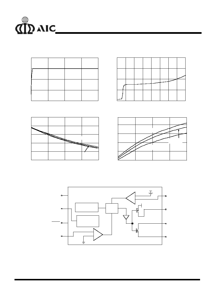
TYPICAL PERFORMANCE CHARACTERISTICS
(T
A
=25
∞
C)
V
IN
(V)
150
200
250
300
350
Source Current (
µ
A)
Fig. 1 V
REF
Source Current vs. V
IN
4
8
12
20
16
V
IN
(V)
0
5
10
15
20
Shutdown Current (
µ
A)
Fig. 2 Shutdown Current vs. V
IN
4
6
8
10
12
14
16
18
20
V
IN
(V)
Duty Cycle (%)
Fig. 3 Duty Cycle vs. V
IN
Voltage
T
A
=
25
∞
C
T
A
=
0
∞
C
4
8
12
16
20
50
60
70
80
90
100
T
A
=
70
∞
C
V
IN
(V)
Frequency (kHz)
Fig. 4 Frequency vs. V
IN
Voltage
4
8
12
16
20
80
130
180
230
280
330
T
A
=0
∞
C
T
A
=25
∞
C
T
A
=70
∞
C
n
BLOCK DIAGRAM
+
-
+
-
ERROR COMPARATOR
LATCH
CURRENT LIMIT
COMPARATOR
1.22V
REFERENCE
VOLTAGE
PFM
OSCILLATOR
VREF
VIN
SHDN
4
3
2
1
FB
OUTPUT DRIVER
V
IN
V
IN
70mV
DHI
DLOW
CL
8
7
6
5
GND
AIC1650
4
n
PIN DESCRIPTIONS
PIN 1: VIN
- Input Supply Voltage (4V~20V)
PIN 2: VREF - Reference Output (1.22V) By-
pass with a 0.047
µ
F capacitor to
GND. Sourcing capability is
guaranteed to be greater than
250
µ
A.
PIN 3:
SHDN - Logic input to shutdown the chip.
>1.5V (normal operation),
GND (shutdown mode)
In shutdown mode DLOW and
DHI pins are at high level.
PIN 4: FB
- Feedback signal input to sense
ground. Connecting a resistor R1
to V
OUT
and a resistor R2 to
V
REF
pin yields the output volt-
age:
V
OUT
= -(R1/R2 ) x V
REF
PIN 5: GND - Power ground.
PIN 6: DLOW - Driver sinking output. Connected
to DHI when using an external P-
channel MOSFET. When using
an external PNP bipolar transis-
tor, connect a resistor RB from
this pin to DHI. RB value de-
pends on V
IN
, inductor and PNP
bipolar transistor. By adjusting
the RB value, efficiency can be
optimized.
PIN 7: DHI
- Driver sourcing output. Connect
to gate of the external P-channel
MOSFET or base of the PNP bi-
polar transistor.
PIN 8: CL
- Current-limit input. This pin
clamps the switch peak current
to prevent over-current damage to
the external switch.
n
APPLICATION INFORMATIONS
4
6
8
10
12
14
16
18
20
V
IN
(V)
0
0.2
0.4
0.6
0.8
1
1.2
1.4
1.6
1.8
Max. Output Power vs V
IN
Max. Output Power (W)
Typical Application Circuit
Inductor Value
100
µ
H
270
µ
H
120
µ
H
150
µ
H
180
µ
H
220
µ
H
300
µ
H
330
µ
H
The typical application circuit generates an adjustable
negative voltage for contrast bias of LCD displays. Effi-
ciency and output power can be optimized by using
appropriate inductor and switch. The following formulas
provide a guideline for determining the optimal com-
ponent values:
L
=
(11.1 0.15
V )
V
I
V
IN
IN
OUT
OUT
-
◊
◊
◊
PNP :
V
V
V
CEO
IN
OUT
>
+
I
200
I
V
C,MAX
OUT
IN
◊
V
I
200
=
I
at
0.4V
V
IN
OUT
C
CE
◊
<
and
10
=
RB
3 x L x (V
IN
- 0.8)
where, V
IN
(V), V
OUT
(V), I
OUT
(A), L(
µ
H), R
B
(
)

AIC1650
5
n
APPLICATION CIRCUIT
(Refer to TYPICAL APPLICATION CIRCUIT)
0
5
10
15
20
25
30
Load Current (mA)
75
80
85
90
95
Fig. 5 Efficiency vs. Load Current
V
OUT
= -15V
L =220
µ
H
V
IN
=13V
V
IN
=18V
Efficiency (%)
V
IN
=8V
4
6
8
10
12
14
16
18
20
V
IN
(V)
80
85
90
95
Fig. 6 Efficiency vs. V
IN
L=300
µ
H
L=220
µ
H
L=150
µ
H
V
OUT
=-15V
I
OUT
=-10mA
Efficiency (%)
0
5
10
15
20
25
30
Load Current (mA)
75
80
85
90
95
Fig. 7 Efficiency vs. Load Current
V
OUT
=-22V
L =220
µ
H
V
IN
=18V
V
IN
=13V
V
IN
=8V
Efficiency (%)
V
IN
(V)
Fig. 8 Efficiency vs. V
IN
Efficiency (%)
4
6
8
10
12
14
16
18
20
80
85
90
95
L=150
µ
H
L=220
µ
H
L=300
µ
H
V
OUT
=-22V
I
OUT
=-10mA
0
5
10
15
20
25
30
Load Current (mA)
75
80
85
90
95
Fig. 9 Efficiency vs. Load Current
V
OUT
= -30V
L = 220
µ
H
V
IN
=18V
V
IN
=13V
V
IN
=8V
Efficiency (%)
V
IN
(V)
Fig. 10 Efficiency vs. V
IN
Efficiency (%)
4
6
8
10
12
14
16
18
20
80
85
90
95
L=300
µ
H
L=220
µ
H
L=150
µ
H
V
OUT
= -30V
I
OUT
= -10mA