 | –≠–ª–µ–∫—Ç—Ä–æ–Ω–Ω—ã–π –∫–æ–º–ø–æ–Ω–µ–Ω—Ç: AIC1652CS | –°–∫–∞—á–∞—Ç—å:  PDF PDF  ZIP ZIP |

AIC1652
MICROPOWER INVERTING DC/DC CONVERTER
SPEC NO: DS-1652-02 DEC 27, 00
ANALOG INTEGRATIONS CORPORATION
www.analog.com.tw
4F, 9 Industry E. 9th Road, Science-based Industrial Park , Hsinchu, Taiwan, R.O.C. TEL: (8863)577-2500 FAX:(8863)577-2510
1
n
FEATURES
l
2.4V to 7V Input Voltage Operation.
l
Adjustable Output Voltage up to -40V.
l
Low Quiescent Current at 80
µ
A.
l
Pulse Frequency Modulation Maintains High
Efficiency (87%).
l
70KHz to 160KHz Switching Frequency.
l
Power-Saving Shutdown Mode (0.7
µ
A Typical).
l
High Efficiency with Low Cost External PNP
Bipolar Transistor.
n
APPLICATIONS
l
Negative LCD Contrast Bias for
1. Notebook & Palmtop Computers.
2. Pen-Based Data System.
3. Portable Data Collection Terminals.
4. Personal Digital Assistants.
l
Negative Voltage Supply.
n
DESCRIPTION
The AIC1652 is a high performance inverting
DC/DC converter, designed to drive an external
power switch to generate programmable negative
voltages. In the particularly suitable LCD bias con-
trast application, efficiency of 87% can be
achieved with low cost PNP bipolar transistor driv-
ers. Output voltage can be scaled to -40V or
greater by two external resistors. A pulse frequen-
cy modulation scheme is employed to maintain
high efficiency conversion under wide input voltage
range. Quiescent current is about 80
µ
A and can
be reduced to 0.7
µ
A in shutdown mode. Switching
frequency being around 70KHz to 160KHz range,
small size switching components are ideal for bat-
tery powered portable equipments, like notebook
and palmtop computers.
n
TYPICAL APPLICATION CIRCUIT
D1 1N5819
AIC1652
CL
DHI
DLOW
FB
GND
SHDN
VIN
VREF
C3
10nF
C4
0.047
µ
F
150
µ
H
*L
Q1
9012
RB
470~1.8K
R1
1M
C2
C1
V
IN
2.4V ~ 7V
V
OUT
-12V~ -40V
-10mA
100
µ
F
*
Sumida CD-54 Series
V
OUT
= -1.22V x R1/R2
100
µ
F
+
+
R2
100K
Negative LCD Contrast Bias Power Supply
n
ORDERING INFORMATION
PACKAGE TYPE
N: PLASTIC DIP
S: SMALL OUTLINE
TEMPERATURE RANGE
C=0
∞
C~+70
∞
C
ORDER NUMBER
AIC1652CN
(PLASTIC DIP)
PIN CONFIGURATION
AIC1652CS
(PLASTIC SO)
TOP VIEW
DLOW
1
3
4
2
8
6
5
7
CL
VREF
SHDN
FB
DHI
GND
VIN
AIC1652 XX
AIC1652
MICROPOWER INVERTING DC/DC CONVERTER
SPEC NO: DS-1652-02 DEC 27, 00
ANALOG INTEGRATIONS CORPORATION
www.analog.com.tw
4F, 9 Industry E. 9th Road, Science-based Industrial Park , Hsinchu, Taiwan, R.O.C. TEL: (8863)577-2500 FAX:(8863)577-2510
2
n
ABSOLUTE MAXIMUM RATINGS
Supply Voltage .....................
................................................ ... ... ... ... ... ... ............
7V
SHDN Voltage
.................................................. ... ... ... ... .....................................
7V
Operation Temperature Range
................................... ... ... ..........................
0
∞
C~70
∞
C
Storage Temperature Range
..
.................................. ... ... ... ................
. -65
∞
C~
150
∞
C
n
TEST CIRCUIT
Refer to Typical Application Circuit.
n
ELECTRICAL CHARACTERISTICS
(V
IN
=5V, Ta=25
∞
C, unless otherwise specified.)
PARAMETER
TEST CONDITIONS
MIN.
TYP.
MAX.
UNIT
Input Voltage
2.4
7
V
Switch Off Current
V
FB
=-50mV
80
150
µ
A
V
REF
Voltage
I
SOURCE
= 250
µ
A
1.16
1.22
1.28
V
V
REF
Source Current
250
µ
A
DLOW "ON Resistance"
5
DHI "ON Resistance"
7
CL Threshold
70
mV
Shutdown Threshold
0.8
1.5
2.4
V
Shutdown Mode Current
V
0V
SHDN
=
0.7
2
µ
A

AIC1652
MICROPOWER INVERTING DC/DC CONVERTER
SPEC NO: DS-1652-02 DEC 27, 00
ANALOG INTEGRATIONS CORPORATION
www.analog.com.tw
4F, 9 Industry E. 9th Road, Science-based Industrial Park , Hsinchu, Taiwan, R.O.C. TEL: (8863)577-2500 FAX:(8863)577-2510
3
n
TYPICAL PERFORMANCE CHARACTERISTICS
2
3
4
5
6
7
8
0
50
100
150
200
250
300
350
V
IN
(V)
Source Current (
µ
A)
V
REF
Source Current vs V
IN
1
2
3
4
5
6
7
8
0
0.5
1
1.5
V
IN
(V)
Shutdown Current (
µ
A)
Shutdown Current vs V
IN
Ta=0
∞
C
70
90
110
130
50
150
V
IN
(V)
Frequency (KHz)
Frequency vs V
IN
Voltage
2
3
4
5
6
7
Ta=25
∞
C
Ta=70
∞
C
2
3
4
5
6
7
80
85
90
95
100
V
IN
(V)
Duty Cycle (%)
Duty Cycle vs V
IN
Voltage
Ta=0
∞
C
Ta=70
∞
C
Ta=25
∞
C
n
BLOCK DIAGRAM
+
-
+
-
ERROR COMPARATOR
LATCH
CURRENT LIMIT
COMPARATOR
1.22V
REFERENCE
VOLTAGE
PFM
OSCILLATOR
VREF
VIN
SHDN
4
3
2
1
FB
OUTPUT DRIVER
V
IN
V
IN
70mV
DHI
DLOW
CL
8
7
6
5
GND
AIC1652
MICROPOWER INVERTING DC/DC CONVERTER
SPEC NO: DS-1652-02 DEC 27, 00
ANALOG INTEGRATIONS CORPORATION
www.analog.com.tw
4F, 9 Industry E. 9th Road, Science-based Industrial Park , Hsinchu, Taiwan, R.O.C. TEL: (8863)577-2500 FAX:(8863)577-2510
4
n
PIN DESCRIPTIONS
PIN 1: VIN
- 2.4V to 7V input supply voltage.
PIN 2: VREF - 1.22V reference output. Bypass with
a 0.047
µ
F capacitor to GND.
Sourcing capability is guaranteed to
be greater than 250
µ
A.
PIN 3:
SHDN - Logic input to shutdown the chip.
>1.5V = normal operation,
GND = shutdown
In shutdown mode DLOW and DHI
pins are at high level.
PIN 4: FB
- Feedback signal input to sense
ground. Connecting a resistor R1 to
V
OUT
and a resistor R2 to V
REF
pin
yields the output voltage:
V
OUT
= -(R1/R2 ) x V
REF
PIN 5: GND - Power ground.
PIN 6: DLOW - Driver sinking output. Connected to
DHI when using an external P-
channel MOSFET. When using an
external PNP bipolar transistor,
connect a resistor RB from this pin
to DHI. RB value depends on V
IN
,
inductor and PNP bipolar transistor.
By adjusting the RB value, efficiency
can be optimized.
PIN 7: DHI
- Driver sourcing output. Connect to
gate of the external P-channel
MOSFET or base of the PNP bipolar
transistor.
PIN 8: CL
- Current-limit input. This pin clamps
the switch peak current to prevent
over-current damage to the external
switch.
n
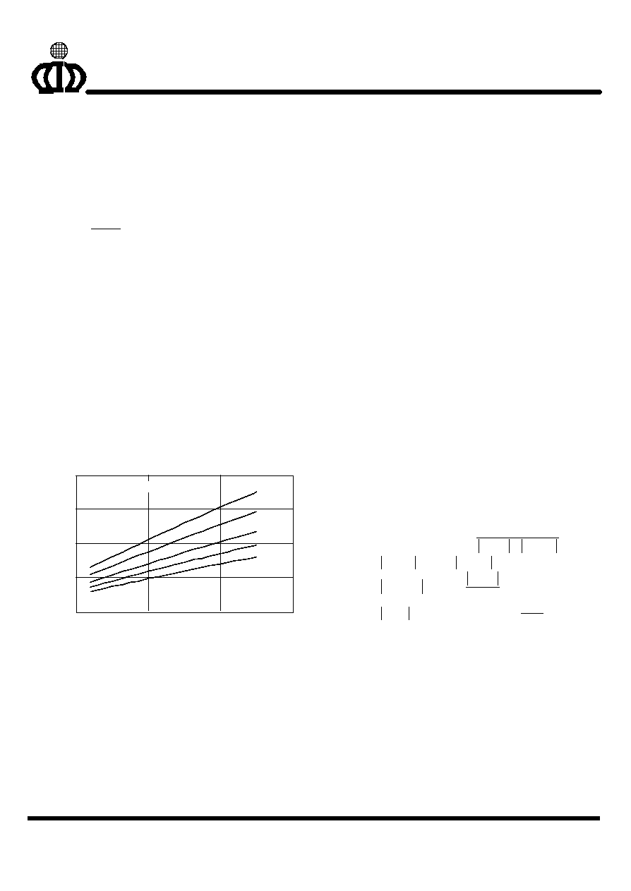
APPLICATION INFORMATIONS
2
4
6
8
0
0.2
0.4
0.6
0.8
100
µ
H
120
µ
H
150
µ
H
180
µ
H
220
µ
H
V
IN
(V)
Max. Output Power vs V
IN
Inductor Value
Typical Application Circuit
Max. Output Power (W)
The typical application circuit generates an adjustable
negative voltage for contrast bias of LCD displays. Effi-
ciency and output power can be optimized by using ap-
propriate inductor and switch. The following formulas
provide a guideline for determining the optimal component
values:
L
=
(11.1 0.15
V )
V
I
V
IN
IN
OUT
OUT
-
◊
◊
◊
PNP :
V
V
V
CEO
IN
OUT
>
+
I
200
I
V
C,MAX
OUT
IN
◊
V
0.4 V at I = 200
I
V
CE
C
OUT
IN
<
◊
and
10
=
RB
3 x L x (V
IN
- 0.8)
where, units: V
IN
& V
OUT
in V, I
OUT
in A, L in
µ
H,
RB in
AIC1652
MICROPOWER INVERTING DC/DC CONVERTER
SPEC NO: DS-1652-02 DEC 27, 00
ANALOG INTEGRATIONS CORPORATION
www.analog.com.tw
4F, 9 Industry E. 9th Road, Science-based Industrial Park , Hsinchu, Taiwan, R.O.C. TEL: (8863)577-2500 FAX:(8863)577-2510
5
n
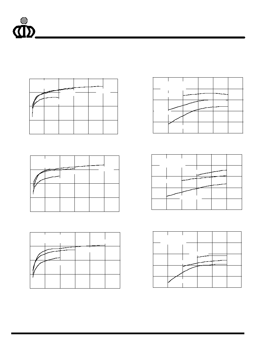
APPLICATION EXAMPLES
0
5
10
15
20
25
30
70
75
80
85
90
Load Current (mA)
Efficiency vs Load Current
V
OUT
= -15V
L
=150
µ
H
V
IN
=5V
V
IN
=7V
V
IN
=3V
Efficiency (%)
2
3
4
5
6
7
8
80
82
84
86
88
90
L=220
µ
H
L=150
µ
H
L=100
µ
H
V
IN
(V)
Efficiency vs V
IN
V
OUT
=
-15V
I
OUT
=
-
10mA
Efficiency (%)
0
5
10
15
20
25
30
70
75
80
85
90
Load Current (mA)
Efficiency vs Load Current
V
OUT
=
-
22V
L
=120
µ
H
V
IN
=3V
V
IN
=7V
V
IN
=5V
Efficiency (%)
2
3
4
5
6
7
8
80
82
84
86
88
90
V
IN
(V)
Efficiency vs V
IN
L=220
µ
H
L=150
µ
H
L=100
µ
H
V
OUT
=
-
22V
I
OUT
=
-
10mA
Efficiency (%)
0
5
10
15
20
25
30
70
75
80
85
90
Load Current (mA)
Efficiency vs Load Current
V
OUT
=
-
30V
L
=100
µ
H
V
IN
=3V
V
IN
=5V
V
IN
=7V
Efficiency (%)
2
3
4
5
6
7
8
80
82
84
86
88
90
V
IN
(V)
Efficiency vs V
IN
Efficiency (%)
L=150
µ
H
L=120
µ
H
L=100
µ
H
V
OUT
=
-30V
I
OUT
=
-
10mA