
ASAHI KASEI
[AK4120]
MS0134-E-00
2002/1
- 1 -
GENERAL DESCRIPTION
The AK4120 is a stereo asynchronous sample rate converter. The input sample rate range is from 8kHz
to 48kHz. The output sample rate is fixed at 32kHz, 44.1kHz, 48kHz or 96kHz. AK4120 includes a
digital mixer and digital volume control. Applications for this device include pro audio mastering,
consumer format conversion and desktop audio production and playback.
FEATURES
o
Stereo Asynchronous Sample Rate Converter
o
Digital Mixer
o
Digital Volume
o
Input Sample Rate Range (FSI): 8kHz to 48kHz
o
Output Sample Rate (FSO): 32kHz, 44.1kHz, 48kHz and 96kHz
o
Input to Output Sample Rate Ratio: FSO/FSI = 0.667 to 6
o
THD+N: �113dB at 1kHz input
o
I/F format: MSB justified (20bit), LSB justified (16bit/20bit), I
2
S
o
Master clock: 256/512fs
o
3-wire Serial or I
2
C Bus �P I/F for mode setting
o
Power Supply: 2.7 to 3.6V
Sample Rate Converter with Mixer and Volume
AK4120
Input#1
Audio
I/F
Sample
Rate
Converter
Input#2
Audio
I/F
Output
Audio
I/F
Volume#1
ILRCK1
IBICK1
SDTI1
ILRCK2
IBICK2
SDTI2
IMCLK1
OLRCK
OBICK
SDTO
OMCLK
VDD
VSS
I2C
PDN
I2MODE
OMODE
CSN/CAD1 CCLK/SDL CDTI/SDA
I2S
IMCLK2
TEST
�
P I/F
CAD0
Volume#2

ASAHI KASEI
[AK4120]
MS0134-E-00
2002/1
- 2 -
n
Ordering Guide
AK4120VF
-40
+85
�
C
24pin VSOP (0.65mm pitch)
AKD4120
Evaluation Board for AK4120
n
Pin Layout
6
5
4
3
2
1
IMCLK1
SDTI1
ILRCK1
IBICK1
TEST
I2S
I2C
7
CAD0
8
IMCLK2
SDTI2
IBICK2
ILRCK2
I2MODE
VDD
VSS
OMODE
Top
View
10
9
CSN/CAD1
CCLK/SCL
CDTI/SDA
11
PDN
12
OMCLK
SDTO
OBICK
OLRCK
19
20
21
22
23
24
18
17
15
16
14
13
ASAHI KASEI
[AK4120]
MS0134-E-00
2002/1
- 3 -
PIN/FUNCTION
No.
Pin Name
I/O
Function
1
IMCLK1
I
Master Clock Input Pin for Input#1
2
SDTI1
I
Audio Serial Data Input Pin for Input#1
3
IBICK1
I
Audio Serial Data Clock Pin for Input#1
4
ILRCK1
I
L/R Clock Pin for Input#1
5
TEST
I
Test Pin. Connect to VSS.
6
I2S
I
Audio I/F Select Pin
"L": Set by Register, "H": I
2
S
7
I2C
I
I
2
C Select Pin. "L": 3-wire, "H": I
2
C
8
CAD0
I
Chip Address 0 Pin
CSN
I
Chip Select Pin in 3wire serial control mode in 3-wire Serial Control Mode.
9
CAD1
I
Chip Address 1 Pin in I
2
C control mode.
CCLK
I
Control Data Clock Pin in 3wire serial control mode in 3-wire Serial Control
Mode.
10
SCL
I
Control Data Clock Pin in I
2
C control mode.
CDTI
I
Control Data Input Pin in 3wire serial control mode in 3-wire Serial Control
Mode.
11
SDA
I/O
Control Data Pin in I
2
C serial control mode in I
2
C control mode.
12
PDN
I
Power-Down pin
When "L", the AK4120 is powered-down and reset.
13
OLRCK
I/O
L/R Clock Pin for Output
14
OBICK
I/O
Audio Serial Data Clock Pin for Output
15
SDTO
O
Audio Serial Data Pin for Output
16
OMCLK
I
Master Clock Pin for Output
17
OMODE
I
Master/Slave select pin for Output Audio Data
"L": Slave, "H": Master
18
VSS
I
Digital Ground Pin
19
VDD
I
Digital Power Supply Pin, 3.3V
20
I2MODE
I
Master/Slave select pin for Input Audio Data #2
"L": Slave, "H": Master
21
ILRCK2
I/O
L/R Clock Pin for Input#2
22
IBICK2
I/O
Audio Serial Data Clock Pin for Input#2
23
SDTI2
I
Audio Serial Data Input Pin for Input#2
24
IMCLK2
I
Master Clock Input Pin for Input#2

ASAHI KASEI
[AK4120]
MS0134-E-00
2002/1
- 4 -
ABSOLUTE MAXIMUM RATINGS
(VSS=0V; Note 1)
Parameter
Symbol
min
max
Units
Power Supplies
VDD
-0.3
4.6
V
Input Current, Any Pin Except Supplies
IIN
-
�
10
mA
Input Voltage
VIN
-0.3
VDD+0.3
V
Ambient Temperature (Power applied)
Ta
-40
85
�
C
Storage Temperature
Tstg
-65
150
�
C
Note 1: All voltages with respect to ground.
WARNING: Operation at or beyond these limits may result in permanent damage to the device.
Normal operation is not guaranteed at these extremes.
RECOMMENDED OPERATING CONDITIONS
(VSS=0V; Note 2)
Parameter
Symbol
min
typ
max
Units
Power Supplies
VDD
2.7
3.3
3.6
V
Note 2: All voltages with respect to ground.
SRC PERFORMANCE
(Ta=-40
85
�
C; VDD = 2.7
3.6V; data = 20bit; measurement bandwidth = 20Hz~ FSO/2; unless otherwise specified.)
Parameter
Symbol
min
typ
max
Units
Resolution
20
Bits
Input Sample Rate (Note 3)
FSI
8
48
kHz
Output Sample Rate (Note 4)
FSO
32
96
kHz
Dynamic Range (Input= 1kHz, -60dBFS, Note 5)
FSO/FSI=44.1kHz/48kHz
FSO/FSI=48kHz/44.1kHz
FSO/FSI=32kHz/48kHz
FSO/FSI=96kHz/32kHz
Worst Case (FSO/FSI=32kHz/48kHz)
Dynamic Range (Input= 1kHz, -60dBFS, A-weighted, Note 5)
FSO/FSI=44.1kHz/48kHz
-
-
-
-
112
-
115
116
114
119
-
117
-
-
-
-
-
-
dB
dB
dB
dB
dB
dB
THD+N (Input= 1kHz, 0dBFS, Note 5)
FSO/FSI=44.1kHz/48kHz
FSO/FSI=48kHz/44.1kHz
FSO/FSI=32kHz/48kHz
FSO/FSI=96kHz/32kHz
Worst Case (FSO/FSI=48kHz/8kHz)
-
-
-
-
-
-112
-113
-111
-111
-
-
-
-
-
-103
dB
dB
dB
dB
dB
Ratio between Input and Output Sample Rate
(FSO/FSI, Note 6, Note 7)
FSO/FSI
0.667
6
-
Note 3. 32kHz~96kHz for INPUT#2 at Path Mode 0. 8kHz~96kHz at Path Mode 2 and 3.
Note 4. Min = 8kHz at Path Mode 2 and 3.
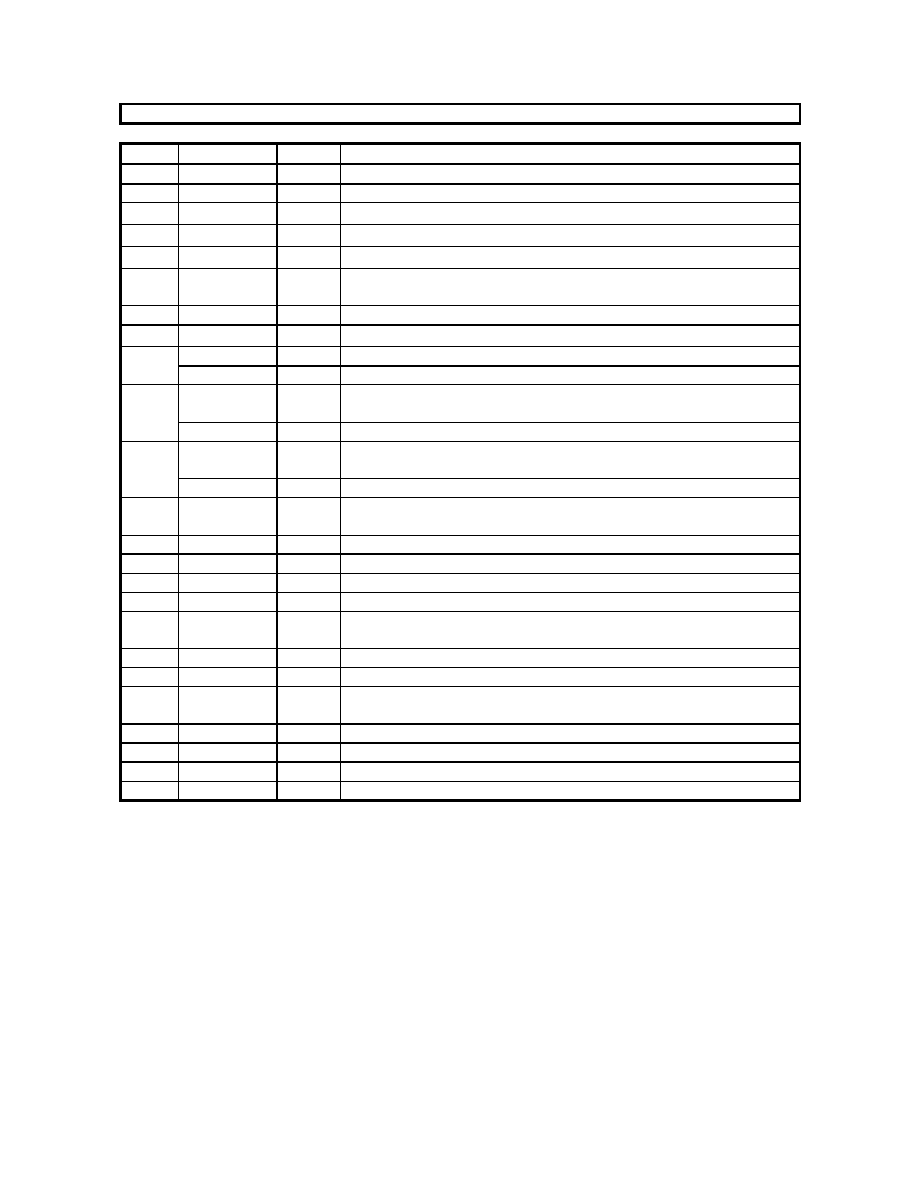
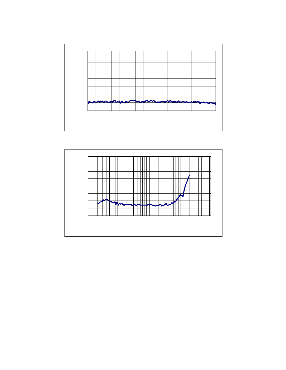
Note 5. Measured by Rohde & Schwarz UPD04, Rejection Filter= wide, 8192point FFT. Refer Figure 1 and Figure 2.
Note 6. The "0.667" is the ratio of FSO/FSI when FSI is 48kHz and FSO is 32kHz
Note 7. The "6" is the ratio when FSI is 8kHz and FSO is 48kHz.
ASAHI KASEI
[AK4120]
MS0134-E-00
2002/1
- 5 -
-115
-113
-111
-109
-107
-105
-103
-101
32
37
42
47
FSI [kHz]
THD+N [dB]
Figure 1: Input Sample Rate (FSI) vs. THD+N (FSO=48kHz)
-120
-115
-110
-105
-100
-95
-90
-85
-80
10
100
1000
10000
100000
Input Frequency [Hz]
THD+N [dB]
Figure 2: Input Frequency vs. THD+N (FSI=44.1kHz, FSO=48kHz)