 | –≠–ª–µ–∫—Ç—Ä–æ–Ω–Ω—ã–π –∫–æ–º–ø–æ–Ω–µ–Ω—Ç: UCN5804B | –°–∫–∞—á–∞—Ç—å:  PDF PDF  ZIP ZIP |
Combining low-power CMOS logic with high-current and high-voltage
bipolar outputs, the UCN5804B and UCN5804LB BiMOS II translator/
drivers provide complete control and drive for a four-phase unipolar stepper-
motor with continuous output current ratings to 1.25 A per phase (1.5 A
startup) and 35 V.
The CMOS logic section provides the sequencing logic, DIRECTION
and OUTPUT ENABLE control, and a power-on reset function. Three
stepper-motor drive formats, wave-drive (one-phase), two-phase, and half-
step are externally selectable. The inputs are compatible with standard
CMOS, PMOS, and NMOS circuits. TTL or LSTTL may require the use of
appropriate pull-up resistors to ensure a proper input-logic high.
The wave-drive format consists of energizing one motor phase at a time
in an A-B-C-D (or D-C-B-A) sequence. This excitation mode consumes the
least power and assures positional accuracy regardless of any winding
inbalance in the motor. Two-phase drive energizes two adjacent phases in
each detent position (AB-BC-CD-DA). This sequence mode offers an
improved torque-speed product, greater detent torque, and is less susceptible
to motor resonance. Half-step excitation alternates between the one-phase
and two-phase modes (A-AB-B-BC-C-CD-D-DA), providing an eight-step
sequence.
The bipolar outputs are capable of sinking up to 1.5 A and withstanding
50 V in the off state (sustaining voltages up to 35 V). Ground-clamp and
flyback diodes provide protection against inductive transients. Thermal
protection circuitry disables the outputs when the chip temperature is exces-
sive.
Both devices are rated for operation over the temperature range of -20
∞C
to +85
∞C. The UCN5804B is supplied in a 16-pin dual in-line plastic batwing
package with a copper lead frame and heat-sinkable tabs for improved power
dissipation capabilities; the UCN5804LB is supplied in a 16-lead plastic
SOIC batwing package with a copper lead frame and heat-sinkable tabs.
FEATURES
I 1.5 A Maximum Output Current
I 35 V Output Sustaining Voltage
I Wave-Drive, Two-Phase, and Half-Step Drive Formats
I Internal Clamp Diodes
I Output Enable and Direction Control
I Power-On Reset
I Internal Thermal Shutdown Circuitry
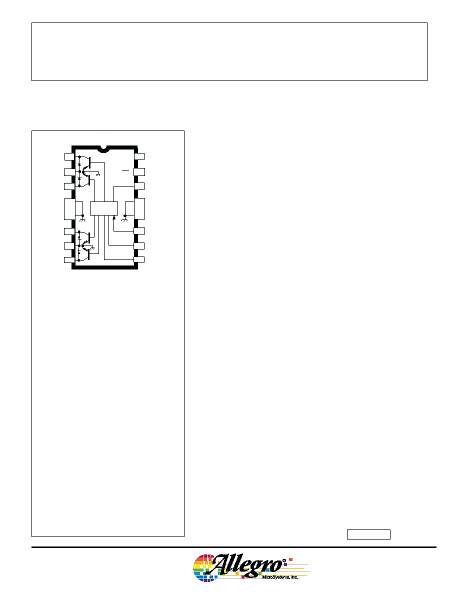
BiMOS II UNIPOLAR
STEPPER-MOTOR TRANSLATOR/DRIVER
Always order by complete part number, e.g., UCN5804B .
Dwg. W-194
SUPPLY
DIRECTION
OUTPUT
ENABLE
GROUND
GROUND
GROUND
GROUND
STEP INPUT
HALF-STEP
ONE-PHASE
OUTPUT
OUTPUT
OUTPUT
OUTPUT
B
BD
D
K
C
AC
A
K
LOGIC
OE
16
DD
V
15
14
13
12
11
10
9
8
7
6
5
4
3
2
1
ABSOLUTE MAXIMUM RATINGS
Output Voltage, V
CE
............................... 50 V
Output Sustaining Voltage,
V
CE (sus)
............................................ 35 V
Output Sink Current, I
OUT
.................... 1.5 A
Logic Supply Voltage, V
DD
.................... 7.0 V
Input Voltage, V
IN
.................................. 7.0 V
Package Power Dissipation,
P
D
......................................... See Graph
Operating Temperature Range,
T
A
.................................. -20
∞
C to +85
∞
C
Storage Temperature Range,
T
S
................................ -55
∞
C to +150
∞
C
Data Sheet
26184.12C*
Note that the UCN5804B (dual in-line package)
and UCN5804LB (small outline IC package) are
electrically identical and share a common
terminal number assignment.
5804

115 Northeast Cutoff, Box 15036
Worcester, Massachusetts 01615-0036 (508) 853-5000
5804
BiMOS II UNIPOLAR
STEPPER-MOTOR
TRANSLATOR/DRIVER
TRUTH TABLE
Drive Format
Pin 9
Pin 10
Two-Phase
L
L
One-Phase
H
L
Half-Step
L
H
Step-Inhibit
H
H
TYPICAL INPUT CIRCUIT
Dwg. EP-021-4
OUT
K
TYPICAL OUTPUT DRIVER
Dwg. EP-010-5
IN
V
DD
Copyright © 1987, 2000 Allegro MicroSystems, Inc.
50
75
100
125
150
5
1
0
ALLOWABLE PACKAGE POWER DISSIPATION IN WATTS
TEMPERATURE IN
∞C
4
3
2
25
Dwg. GP-049-2A
R = 6.0
∞C/W
JT
SUFFIX 'B', R = 43
∞C/W
JA
SUFFIX 'LB', R = 63
∞C/W
JA
5804
BiMOS II UNIPOLAR
STEPPER-MOTOR
TRANSLATOR/DRIVER
www.allegromicro.com
ELECTRICAL CHARACTERISTICS at T
A
= 25
∞
C, T
J
150
∞
C, V
DD
= 4.5 V to 5.5 V
(unless otherwise noted).
Limits
Characteristic
Symbol
Test Conditions
Min.
Typ.
Max.
Units
Output Leakage Current
I
CEX
V
OUT
= 50 V
--
10
50
µA
Output Sustaining Voltage
V
CE(sus)
I
OUT
= 1.25 A, L = 3 mH
35
--
--
V
Output Saturation Voltage
V
CE(SAT)
I
OUT
= 700 mA
--
1.0
1.2
V
I
OUT
= 1 A
--
1.1
1.4
V
I
OUT
= 1.25 A
--
1.2
1.5
V
Clamp Diode Leakage Current
I
R
V
R
= 50 V
--
10
50
µA
Clamp Diode Forward Voltage
V
F
I
F
= 1.25 A
--
1.5
3.0
V
Input Current
I
IN(1)
V
IN
= V
DD
--
0.5
5.0
µA
I
IN(0)
V
IN
= 0.8 V
--
-0.5
-5.0
µA
Input Voltage
V
IN(1)
V
DD
= 5 V
3.5
--
5.3
V
V
IN(0)
-0.3
--
0.8
V
Supply Current
I
DD
2 Outputs ON
--
20
30
mA
Turn-Off Delay
t
ON
50% Step Inputs to 50% Output
--
--
10
µs
Turn-On Delay
t
OFF
50% Step Inputs to 50% Output
--
--
10
µs
Thermal Shutdown Temperature
T
J
--
165
--
∞C
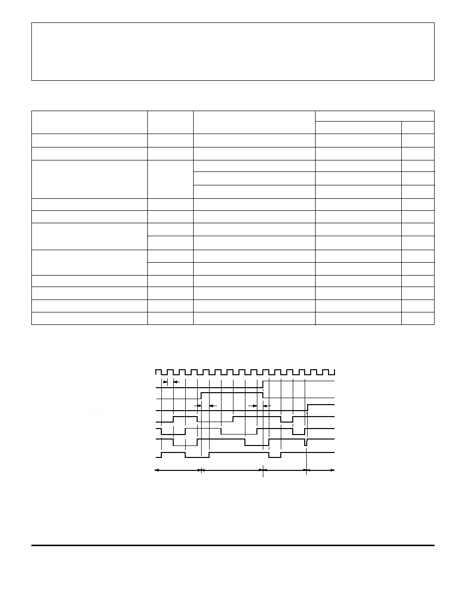
TIMING CONDITIONS
A. Minimum Data Set Up Time . . . . . . . . . . . . . . . . . . . . . . . . 100 ns
B. Minimum Data Hold Time . . . . . . . . . . . . . . . . . . . . . . . . . . 100 ns
C. Minimum Step Input Pulse Width . . . . . . . . . . . . . . . . . . . . . 3.0
µ
s
Dwg. W-110A
ONE PHASE
HALF STEP
OUTPUT A
OUTPUT B
OOUTPUT ENABLE
OUTPUT C
OUTPUT D
TWO -PHASE HALF-STEP WAVE DRIVE
OUTPUT
DISABLED
A
B
C
CLOCK
115 Northeast Cutoff, Box 15036
Worcester, Massachusetts 01615-0036 (508) 853-5000
5804
BiMOS II UNIPOLAR
STEPPER-MOTOR
TRANSLATOR/DRIVER
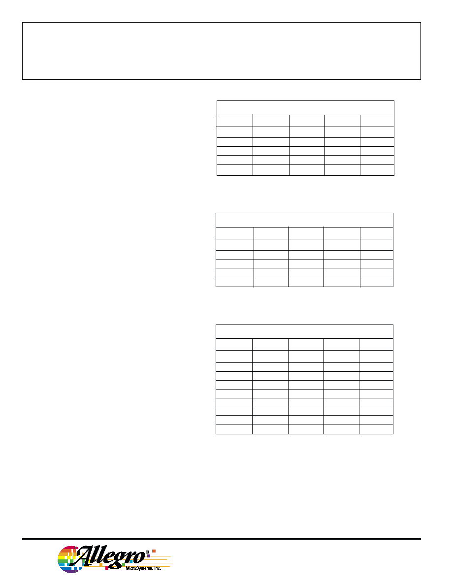
WAVE-DRIVE SEQUENCE
Half Step = L, One Phase = H
Step
A
B
C
D
POR
ON
OFF
OFF
OFF
1
ON
OFF
OFF
OFF
2
OFF
ON
OFF
OFF
3
OFF
OFF
ON
OFF
4
OFF
OFF
OFF
ON
TWO-PHASE DRIVE SEQUENCE
Half Step = L, One Phase = L
Step
A
B
C
D
POR
ON
OFF
OFF
ON
1
ON
OFF
OFF
ON
2
ON
ON
OFF
OFF
3
OFF
ON
ON
OFF
4
OFF
OFF
ON
ON
HALF-STEP DRIVE SEQUENCE
Half Step = H, One Phase = L
Step
A
B
C
D
POR
ON
OFF
OFF
OFF
1
ON
OFF
OFF
OFF
2
ON
ON
OFF
OFF
3
OFF
ON
OFF
OFF
4
OFF
ON
ON
OFF
5
OFF
OFF
ON
OFF
6
OFF
OFF
ON
ON
7
OFF
OFF
OFF
ON
8
ON
OFF
OFF
ON
APPLICATIONS INFORMATION
Internal power-on reset (POR) circuitry resets
OUTPUT
A
(and OUTPUT
D
in the two-phase
drive format) to the on state with initial applica-
tion of the logic supply voltage. After reset, the
circuit then steps according to the tables.
The outputs will advance one sequence
position on the high-to-low transition of the STEP
INPUT pulse. Logic levels on the HALF-STEP
and ONE-PHASE inputs will determine the drive
format (one-phase, two-phase, or half-step). The
DIRECTION pin determines the rotation se-
quence of the outputs. Note that the STEP
INPUT must be in the low state when changing
the state of ONE-PHASE, HALF-STEP, or
DIRECTION to prevent erroneous stepping.
All outputs are disabled (off) when OUTPUT
ENABLE is at a logic high. If the function is not
required, OUTPUT ENABLE should be tied low.
In that condition, all outputs depend only on the
state of the step logic.
During normal commutation of a unipolar
stepper motor, mutual coupling between the
motor windings can force the outputs of the
UCN5804B below ground. This condition will
cause forward biasing of the collector-to-substrate
junction and source current from the output. For
many L/R applications, this substrate current is
high enough to adversely affect the logic circuitry
and cause misstepping. External series diodes
(Schottky are recommended for increased
efficiency at low-voltage operation) will prevent
substrate current from being sourced through the
outputs. Alternatively, external ground clamp
diodes will provide a preferred current path from
ground when the outputs are pulled below ground.
Internal thermal protection circuitry disables
all outputs when the junction temperature reaches
approximately 165
∞C. The outputs are enabled
again when the junction cools down to approxi-
mately 145
∞C.
5804
BiMOS II UNIPOLAR
STEPPER-MOTOR
TRANSLATOR/DRIVER
www.allegromicro.com
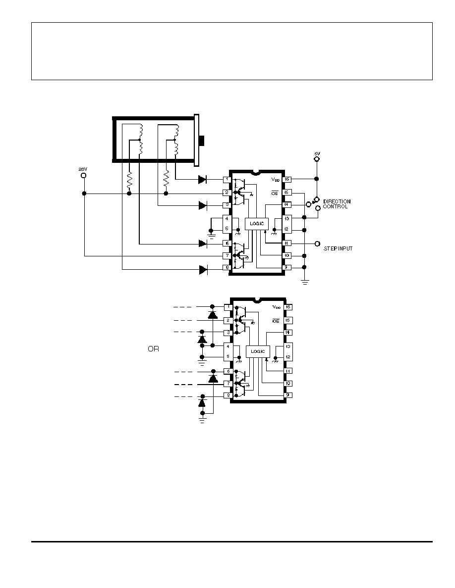
TYPICAL APPLICATION
L/R Stepper-Motor Drive
The products described here are manufactured under one or more
U.S. patents or U.S. patents pending.
Allegro MicroSystems, Inc. reserves the right to make, from time to
time, such departures from the detail specifications as may be
required to permit improvements in the performance, reliability, or
manufacturability of its products. Before placing an order, the user is
cautioned to verify that the information being relied upon is current.
Allegro products are not authorized for use as critical components
in life-support devices or systems without express written approval.
The information included herein is believed to be accurate and
reliable. However, Allegro MicroSystems, Inc. assumes no responsi-
bility for its use; nor for any infringement of patents or other rights of
third parties which may result from its use.