 | –≠–ª–µ–∫—Ç—Ä–æ–Ω–Ω—ã–π –∫–æ–º–ø–æ–Ω–µ–Ω—Ç: UCN5815 | –°–∫–∞—á–∞—Ç—å:  PDF PDF  ZIP ZIP |
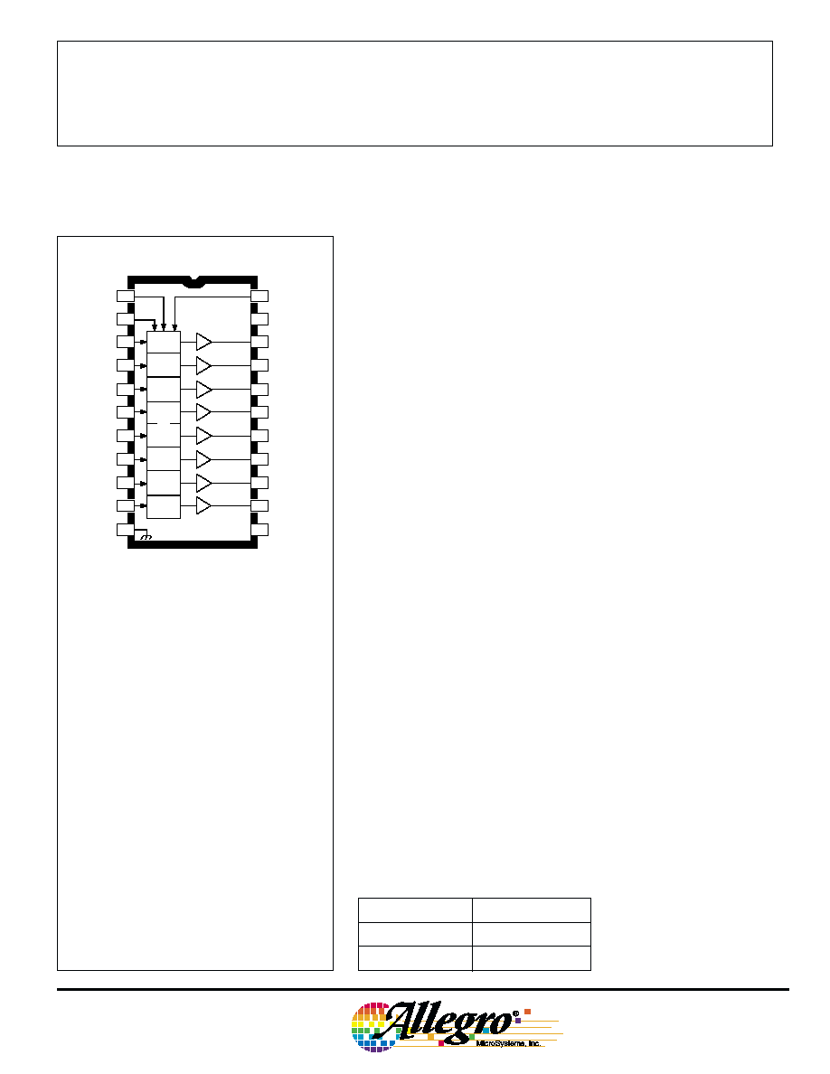
Designed primarily for use with high-voltage vacuum-fluorescent
displays, the UCN5815A and UCN5815EP BiMOS II integrated
circuits consist of eight npn Darlington source drivers with output pull-
down resistors, a CMOS latch for each driver, and common STROBE,
BLANKING, and ENABLE functions.
BiMOS II devices have considerably better data-input rates than
the original BiMOS circuits. With a 5 V logic supply, they will operate
to at least 4.4 MHz. With a 12 V supply, significantly higher speeds
are obtained. The CMOS inputs cause minimum loading and are
compatible with standard CMOS and NMOS logic commonly found in
microprocessor designs. TTL circuits may require the use of appropri-
ate pull-up resistors.
The bipolar outputs may be used as segment, dot (matrix), bar, or
digit drivers in vacuum-fluorescent displays. All eight outputs can be
activated simultaneously at ambient temperatures in excess of 75
∞C.
To simplify printed wiring board layout, output connections are
opposite the inputs. A minimum component display subsystem,
requiring few or no discrete components, can be assembled using the
UCN5815A/EP with the UCN5810AF/EPF/LWF, UCN5812AF/EPF,
or UCN5818AF/EPF serial-to-parallel latched drivers.
Suffix `A' devices are furnished in a standard 22-pin plastic DIP;
suffix `EP' indicates a 28-lead PLCC.
BiMOS II 8-BIT
LATCHED SOURCE DRIVERS
UCN5815A
FEATURES
I To 4.4 MHz Date-lnput Rate
I High-Voltage Source Outputs
I CMOS, NMOS, TTL Compatible Inputs
I Low-Power CMOS Latches
I Internal Pull-Down Resistors
I Wide Supply-Voltage Range
Always order by complete part number:
Part Number
Package
UCN5815A
22-Pin DIP
UCN5815EP
28-Lead PLCC
ABSOLUTE MAXIMUM RATINGS
at +25
∞C Free-Air Temperature
Output Voltage, V
OUT
. . . . . . . . . . . . . . 60 V
Logic Supply Voltage Range,
V
DD
. . . . . . . . . . . . . . . . . . 4.5 V to 15 V
Load Supply Voltage Range,
V
BB
. . . . . . . . . . . . . . . . . . 5.0 V to 60 V
Input Voltage Range,
V
IN
. . . . . . . . . . . -0.3 V to V
DD
+ 0.3 V
Continuous Output Current,
I
OUT
. . . . . . . . . . . . . . . . . . . . . . -40 mA
Package Power Dissipation, P
D
(UCN5815A) . . . . . . . . . . . . . . . 2.5 W*
(UCN5815EP) . . . . . . . . . . . . . 2.27 W*
Operating Temperature Range,
T
A
. . . . . . . . . . . . . . . . . -20
∞
C to +85
∞
C
Storage Temperature Range,
T
S
. . . . . . . . . . . . . . . . -55
∞
C to +150
∞
C
* Derate linearly to 0 W at +150
∞C.
Caution: CMOS devices have input static
protection but are susceptible to damage
when exposed to extremely high static
electrical charges.
Data Sheet
26183.10A*
5815
2
21
22
LOGIC
SUPPLY
ENABLE
1
BLANKING
STROBE
V
DD
3
4
5
6
7
16
17
18
19
20
OUT
1
OUT
2
OUT
3
OUT
4
IN
1
IN
2
IN
3
IN
4
7
8
9
10
11
12
13
14
15
GROUND
OUT
5
OUT
6
OUT
7
Dwg. PP-015-3
OUT
8
LOAD
SUPPLY
IN
5
IN
6
IN
7
IN
8
LATCHES
V
BB
5815
BiMOS II
8-BIT LATCHED
SOURCE DRIVERS
115 Northeast Cutoff, Box 15036
Worcester, Massachusetts 01615-0036 (508) 853-5000
ELECTRICAL CHARACTERISTICS at T
A
= +25
∞
C, V
BB
= 60 V, V
DD
= 5 V and 12 V
(unless otherwise noted).
Limits
Characteristic
Symbol
Test Conditions
Min.
Max.
Units
Output Off Voltage
V
OUT
--
1.0
V
Output On Voltage
V
OUT
I
OUT
= -25 mA, V
BB
= 60 V
57.5
--
V
Output Pull-Down Current
I
OUT
V
OUT
= V
BB
400
850
µA
Output Leakage Current
I
OUT
T
A
= 70
∞C
--
-15
µA
Input Voltage
V
IN(1)
V
DD
= 5.0 V
3.5
5.3
V
V
DD
= 12 V
10.5
12.3
V
V
IN(0)
-0.3
+0.8
V
Input Current
I
IN(1)
V
DD
= V
IN
= 5.0 V
--
100
µA
V
DD
= V
IN
= 12 V
--
240
µA
Input lmpedance
Z
IN
V
DD
= 5.0 V
50
--
k
Supply Current
l
BB
All outputs on, All outputs open
--
10.5
mA
All outputs off, All outputs open
--
100
µA
l
DD
V
DD
= 5.0 V, All outputs off, All inputs = 0 V
--
100
µA
V
DD
= 12 V, All outputs off, All inputs = 0 V
--
200
µA
V
DD
= 5.0 V, One output on, All inputs = 0 V
--
1.0
mA
V
DD
= 12 V, One output on, All inputs = 0 V
--
3.0
mA
NOTE: Positive (negative) current is defined as going into (coming out of) the specified device pin.
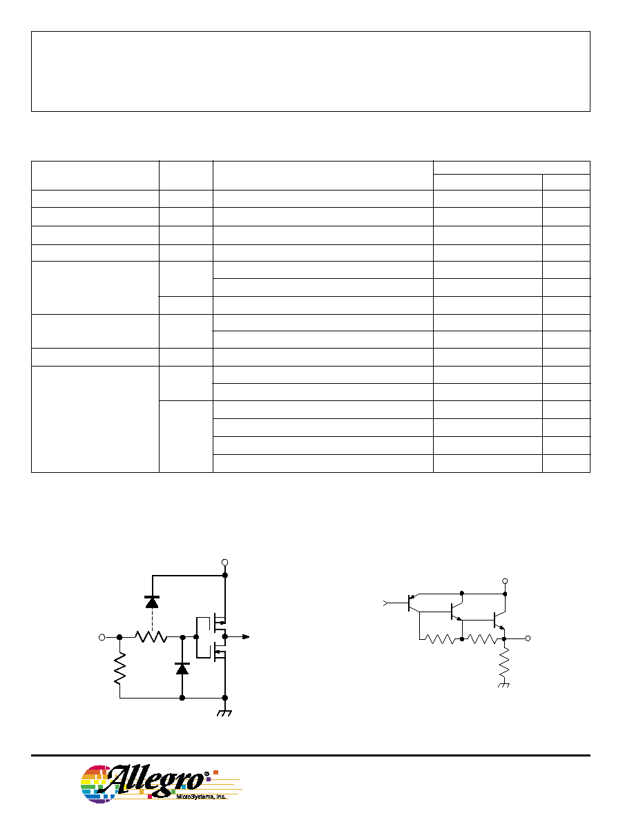
TYPICAL INPUT
CIRCUIT
TYPICAL OUTPUT
DRIVER
IN
V
DD
Dwg. No. EP-010-4A
Dwg. No. EP-021-3
OUT
100 K
VBB
Copyright © 1984, 2000 Allegro MicroSystems, Inc.
5815
BiMOS II
8-BIT LATCHED
SOURCE DRIVERS
UCN5815EP
Dwg. No. A-14,357
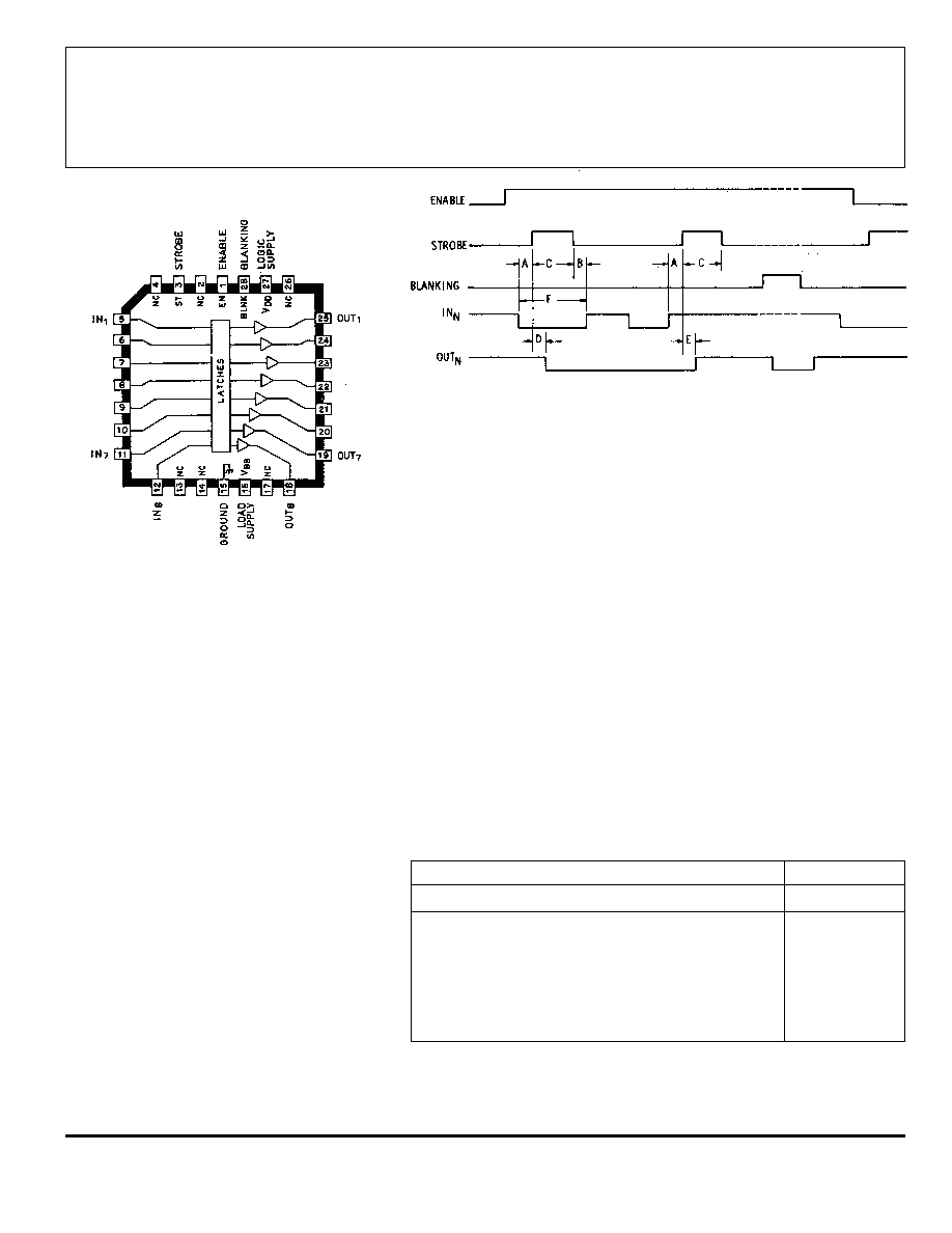
Information present at an input is trans-
ferred to its latch when the STROBE and
ENABLE are high. The latches will continue
to accept new data as long as both STROBE
and ENABLE are held high. With either
STROBE or ENABLE in the low state, no
information can be loaded into the latches.
When the BLANKING input is high, all
of the output buffers are disabled (off)
without affecting the information stored in
the latches. With the BLANKING input low,
the outputs are controlled by the state of the
latches.
Dwg. No. A-10,991
TIMING CONDITIONS
(V
DD
= 5 V, T
A
= +25
∞C, Logic Levels are V
DD
and Ground)
A.
Minimum Data Active Time Before Strobe Enabled
(Data Set-Up Time) . . . . . . . . . . . . . . . . . . . . . . . . . . . . . . . . . . 50 ns
B.
Minimum Data Active Time After Strobe Disabled
(Data Hold Time) . . . . . . . . . . . . . . . . . . . . . . . . . . . . . . . . . . . . 50 ns
C.
Minimum Strobe Pulse Width . . . . . . . . . . . . . . . . . . . . . . . . . . . . . 125 ns
D.
Typical Time Between Strobe Activation and Output
ON to OFF Transition . . . . . . . . . . . . . . . . . . . . . . . . . . . . . . . . . 5.0
µ
s
E.
Typical Time Between Strobe Activation and Output
OFF to ON Transition . . . . . . . . . . . . . . . . . . . . . . . . . . . . . . . . 500 ns
F.
Minimum Data Pulse Width . . . . . . . . . . . . . . . . . . . . . . . . . . . . . . . 225 ns
INPUTS
OUT
N
IN
N
STROBE
ENABLE
BLANK
T-1
T
0
1
1
0
X
0
1
1
1
0
X
1
X
X
X
1
X
0
X
0
X
0
1
1
X
0
X
0
0
0
X
X
0
0
1
1
X
X
0
0
0
0
X = irrelevant
T-1 = previous output state
T = present output state
TRUTH TABLE
Timing is representative of a 4.4 MHz data input rate. Higher speeds may be
attainable with increased supply voltage; operation at high temperatures will
reduce the specified maximum clock frequency.
5815
BiMOS II
8-BIT LATCHED
SOURCE DRIVERS
115 Northeast Cutoff, Box 15036
Worcester, Massachusetts 01615-0036 (508) 853-5000
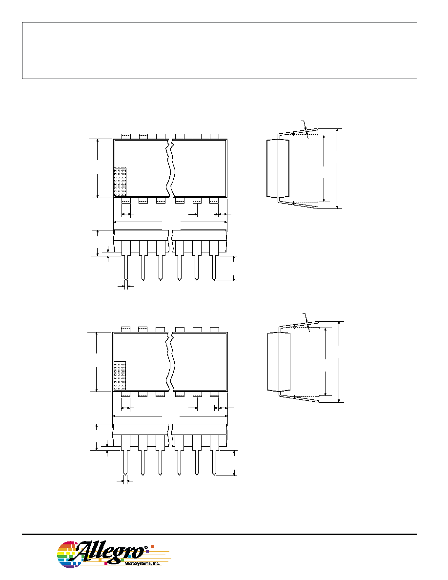
UCN5815A
Dimensions in Inches
(cvontrolling dimensions)
Dimensions in Millimeters
(for reference only)
NOTES: 1. Exact body and lead configuration at vendor's option within limits shown.
2. Lead spacing tolerance is non-cumulative.
3. Lead thickness is measured at seating plane or below.
4. Supplied in standard sticks/tubes of 17 devices.
22
1
2
3
11
0.380
0.330
0.210
MAX
0.070
0.030
0.015
MIN
0.022
0.014
0.100
BSC
0.005
MIN
0.160
0.115
0.015
0.008
0.400
BSC
Dwg. MA-002-22 in
0.500
MAX
12
1.120
1.050
22
1
2
3
11
9.65
8.39
5.33
MAX
0.070
0.030
28.44
26.67
0.39
MIN
0.558
0.356
2.54
BSC
0.13
MIN
4.06
2.93
0.381
0.204
10.16
BSC
Dwg. MA-002-22 mm
12.70
MAX
12

5815
BiMOS II
8-BIT LATCHED
SOURCE DRIVERS
UCN5815EP
Dimensions in Inches
(controlling dimensions
NOTES: 1. Exact body and lead configuration at vendor's option within limits shown.
2. Lead spacing tolerance is non-cumulative.
3. Supplied in standard sticks/tubes of 38 devices or add "TR" to part number for tape and reel.
Dimensions in Millimeters
(for reference only)
18
12
0.020
MIN
0.050
BSC
1
28
INDEX AREA
Dwg. MA-005-28A in
0.026
0.032
0.013
0.021
26
25
19
11
4
5
0.165
0.180
0.495
0.485
0.456
0.450
0.495
0.485
0.456
0.450
0.219
0.191
0.219
0.191
0.51
MIN
4.57
4.20
1.27
BSC
12.57
12.32
11.582
11.430
1
28
INDEX AREA
Dwg. MA-005-28A mm
0.812
0.661
0.331
0.533
12.57
12.32
26
25
19
18
12
11
4
5
11.58
11.43
5.56
4.85
5.56
4.85