
ASM809, ASM810
Alliance Semiconductor
2575 Augustine Drive . Santa Clara, CA 95054 . Tel: 408.855.4900 . Fax: 408.855.4999 . www.alsc.com
Notice: The information in this document is subject to change without notice
October 2003
rev 1.0
3 Pin Microcontroller Power Supply Supervisor
General Description
The ASM809/ASM810 are cost effective 3.0V, 3.3V and 5.0V
power supply supervisor circuits optimized for low-power
microprocessor (µP), microcontroller (µC) and digital systems.
They provide a reset output during power-up, power-down and
brown-out conditions. They provide excellent reliability by
eliminating external components and adjustments. The
ASM809/810 are improved drop-in replacements for the Maxim
MAX809/810 and feature 60% lower supply current.
A reset signal is issued if the power supply voltage drops below
a preset reset threshold and is asserted for at least 140ms after
the supply has risen above the reset threshold. The ASM809
has an active-low RESET output that is guaranteed to be in the
correct logic state for V
CC
down to 1.1V. The ASM810 has an
active-high RESET output. The reset comparator is designed to
ignore fast transients on V
CC
.
Low supply current makes the ASM809/ASM810 ideal for use
in portable and battery operated equipment. The
ASM809/ASM810 are available in a compact, industry standard
3-pin SOT23 package.
Six voltage thresholds are available to support 3V to 5V
systems:
Features:
∑
Monitor 5V, 3.3V and 3V supplies
∑
140ms min. reset pulse width
∑
Active-low reset valid with 1.1V supply (ASM809)
∑
Small 3-pin SOT-23 package
∑
No external components
∑
Specified over full temperature range - -40∞C to 105∞C
RESET THRESHOLD
Suffix
Voltage
L
4.63
M
4.38
J
4.00
T
3.08
S
2.93
R
2.63
Applications
∑
Embedded controllers
∑
Portable/Battery operated systems
∑
Intelligent instruments
∑
Wireless communication systems
∑
PDAs and handheld equipment
∑
Computers
Typical Operating Circuit
V
CC
V
CC
V
CC
µP
RESET
Input
RESET
(RESET)
GND
GND
(RESET)

2 of 10
Notice: The information in this document is subject to change without notice
3 Pin Microcontroller Power Supply Supervisor
ASM809, ASM810
October 2003
rev 1.0
Pin Diagram
Block Diagram
Pin Description
Pin #
Pin
Name
Function
ASM809
ASM810
1
-
GND
Ground.
2
-
RESET
RESET is asserted LOW if V
CC
falls below V
TH
and remains LOW for T
RST
after V
CC
exceeds the
threshold.
-
2
RESET
RESET is asserted HIGH if V
CC
falls below V
TH
and remains HIGH for T
RST
after V
CC
exceeds the
threshold.
3
-
V
CC
Power supply input voltage (3.0V, 3.3V, 5.0V).
Detailed Description
A proper reset input enables a microprocessor /
microcontroller to start in a known state. ASM809/810 assert
reset to prevent code execution errors during power-up,
power-down and brown-out conditions.
Reset Timing
The reset signal is asserted- LOW for the ASM809 and HIGH
for the ASM810- when the V
CC
supply voltage falls below the
threshold trip voltage and remains asserted for 140ms
minimum after the V
CC
has risen above the threshold.
1
2
3
SOT23
ASM809
(ASM810)
GND
RESET
V
CC
(RESET)
ASM809
ASM810
RESET
RESET
0V
5V
0V
5V
0V
5V
V
CC
V
TH
T
RST
Figure 1: Reset TIming Diagram
+
-
RESET Generator
-
+
V
CC
RESET
(RESET)
GND
ASM809
(ASM810)
4.38V
4.00V
3.08V
2.93V
2.63V
4.63V

3 of 10
Notice: The information in this document is subject to change without notice
3 Pin Microcontroller Power Supply Supervisor
ASM809, ASM810
October 2003
rev 1.0
Application Information
Negative V
CC
Transients
The ASM809/810 protect µPs from brownouts and low V
CC
.
Short duration transients of 100mV amplitude and 20µs or
less duration typically do not cause a false RESET.
Valid Reset with V
CC
under 1.1V
When V
CC
is under 1.1V, to ensure logic inputs connected to
the ASM809 RESET pin are in a known state, a 100k
pull-
down resistor is needed at RESET . The value of the resistor
is not critical. A 100k
pull-up resistor to V
CC
at RESET is
needed with the ASM810.
Bidirectional Reset Pin Interfacing
The ASM809/810 can interface with µP / µC bi-directional
reset pins by connecting a 4.7k
resistor in series with the
ASM809/810 reset output and the µP/µC bi-directional reset
pin.
V
CC
Power Supply
ASM809
RESET
GND
100k
V
CC
Power Supply
ASM810
RESET
GND
100k
Power supply
BUF
Buffered
RESET
V
CC
ASM809
GND
GND
RESET
RESET
Input
µC or µP
4.7k
Bi-directional I/O Pin
Figure 2: RESET valid with V
CC
under 1.1V
Figure 3: RESET valid with V
CC
under 1.1V
Figure 4: Bidirectional Reset Pin Interfacing

ASM809, ASM810
4 of 10
Notice: The information in this document is subject to change without notice
3 Pin Microcontroller Power Supply Supervisor
October 2003
rev 1.0
Absolute Maximum Ratings Table 1:
Absolute Maximum Ratings Table 2:
Parameter
Min
Max
Units
Pin Terminal Voltage With Respect To Ground
V
CC
-0.3
6.0
V
RESET, RESET
-0.3
V
CC
+ 0.3
V
Input current at V
CC
20
mA
Output current: RESET, RESET
20
mA
Rate of Rise at V
CC
100
V/µs
Note: These are stress ratings only and the functional operation is not implied. Exposure
to absolute maximum ratings for prolonged time periods may affect device reliability.
Parameter
Min
Max
Units
Power Dissipation (T
A
= 70∞C)
320
uW
Operating temperature range
-40
105
∞C
Storage temperature range
-65
160
∞C
Lead temperature (Soldering, 10 sec)
300
∞C
Note: These are stress ratings only and the functional operation is not implied. Exposure to absolute
maximum ratings for prolonged time periods may affect device reliability.
ASM809, ASM810
5 of 10
Notice: The information in this document is subject to change without notice
3 Pin Microcontroller Power Supply Supervisor
October 2003
rev 1.0
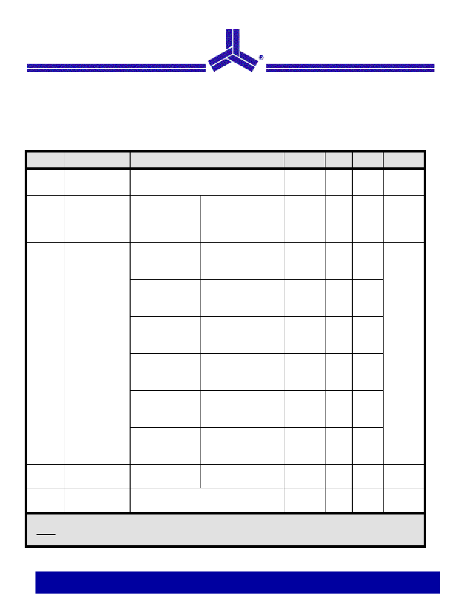
Electrical Characteristics:
Unless otherwise noted, V
CC
is over the full voltage range, T
A
= -40∞C to 105∞C.
Typical values at T
A
= 25∞C, V
CC
= 5V for L/M/J devices, V
CC
= 3.3V for T/S devices and V
CC
= 3V for R devices.
Symbol
Parameter
Conditions
Min
Typ
Max
Unit
V
CC
Input Voltage
Range
T
A
= 0∞C to 70∞C
T
A
= -40∞C to 105∞C
1.1
1.2
5.5
5.5
V
V
I
CC
Supply Current
T
A
= -40∞C to 85∞C
T
A
= -40∞C to 85∞C
T
A
= 85∞C to 105∞C
T
A
= 85∞C to 105∞C
V
CC
< 5.5V, L/M/J
V
CC
< 3.6V, R/S/T
V
CC
< 5.5V, L/M/J
V
CC
< 3.6V, R/S/T
9
6.8
15
10
25
20
µA
V
TH
Reset Threshold
L devices
T
A
= 25∞C
T
A
= -40∞C to 85∞C
T
A
= 85∞C to 105∞C
4.56
4.50
4.40
4.63
4.70
4.75
4.86
V
M devices
T
A
= 25∞C
T
A
= -40∞C to 85∞C
T
A
= 85∞C to 105∞C
4.31
4.25
4.16
4.38
4.45
4.50
4.56
J devices
T
A
= 25∞C
T
A
= -40∞C to 85∞C
T
A
= 85∞C to 105∞C
3.93
3.89
3.80
4.00
4.06
4.10
4.20
T devices
T
A
= 25∞C
T
A
= -40∞C to 85∞C
T
A
= 85∞C to 105∞C
3.04
3.00
2.92
3.08
3.11
3.15
3.23
S devices
T
A
= 25∞C
T
A
= -40∞C to 85∞C
T
A
= 85∞C to 105∞C
2.89
2.85
2.78
2.93
2.96
3.00
3.08
R devices
T
A
= 25∞C
T
A
= -40∞C to 85∞C
T
A
= 85∞C to 105∞C
2.59
2.55
2.50
2.63
2.66
2.70
2.76
Reset Threshold
Temp Coefficient
30
ppm/∞C
V
CC
to Reset
Delay
V
CC
= V
TH
to V
TH
-100mV
60
µs
Notes:
1. Production testing done at T
A
= 25∞C. Over-temperature specifications guaranteed by design only, using six sigma design limits.
2. RESET output is active LOW for the ASM809 and RESET output is active HIGH for the ASM810.