ASM811, ASM812
Alliance Semiconductor
2575 Augustine Drive . Santa Clara, CA 95054 . Tel: 408.855.4900 . Fax: 408.855.4999 . www.alsc.com
Notice: The information in this document is subject to change without notice
October 2003
rev 1.0
4 Pin µP Voltage Supervisor with Manual Reset
General Description
The ASM811/ASM812 are cost effective low power supervisors
designed to monitor voltage levels of 3.0V, 3.3V and 5.0V
power supplies in low-power microprocessor (µP),
microcontroller (µC) and digital systems. They provide excellent
reliability by eliminating external components and adjustments.
A reset signal is issued if the power supply voltage drops below
a preset reset threshold and is asserted for at least 140ms after
the supply has risen above the reset threshold. The ASM811
has an active-low output RESET that is guaranteed to be in the
correct state for V
CC
down to 1.1V. The ASM812 has an active-
high RESET output. The reset comparator is designed to ignore
fast transients on V
CC
. A debounced manual reset input allows
the user to manually reset the systems to bring them out of
locked state.
Low power consumption makes the ASM811/ASM812 ideal for
use in portable and battery operated equipment. The ASM811/
ASM812 are available in a compact 4-pin SOT-143 package
and thus use minimal board space.
Six voltage thresholds are available to support 3V to 5V
systems:
Features
∑
New 4.0V threshold option
∑
9µA supply current
∑
Monitor 5V, 3.3V and 3V supplies
∑
Manual reset input
∑
140ms min. reset pulse width
∑
Guaranteed over temperature
∑
Active-low reset valid with 1.1V supply (ASM811)
∑
Small 4-pin SOT-143 package
∑
No external components
∑
Power-supply transient-immune design
RESET THRESHOLD
Suffix
Voltage
L
4.63
M
4.38
J
4.00
T
3.08
S
2.93
R
2.63
Applications
∑
Computers and Controllers
∑
Embedded controllers
∑
Portable/Battery operated systems
∑
Intelligent instruments
∑
Wireless communication systems
∑
PDAs and handheld equipment
∑
Automotive systems
∑
Safety Systems
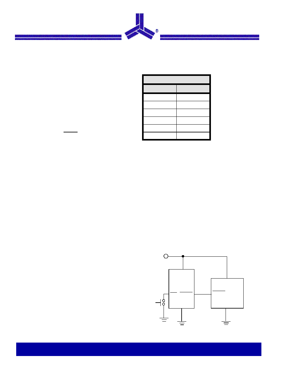
Typical Operating Circuit
V
CC
V
CC
V
CC
µP
RESET
Input
RESET
(RESET)
GND
GND
(RESET)
MR

2 of 10
Notice: The information in this document is subject to change without notice
4 Pin µP Voltage Supervisor with Manual Reset
ASM811, ASM812
October 2003
rev 1.0
Pin Diagram:
Block Diagram
Pin Description
Pin #
Pin
Name
Function
ASM811
ASM812
1
1
GND
Ground.
2 -
RESET
RESET is asserted LOW if V
CC
falls below V
TH
and remains LOW for T
RST
after V
CC
exceeds
the Threshold. In addition, RESET is active LOW as long as the manual reset is low.
-
2
RESET
RESET is asserted HIGH if V
CC
falls below V
TH
and remains HIGH for T
RST
after V
CC
exceeds
the threshold. In addition, RESET is active HIGH as long as the manual reset is low.
3
3
MR
Manual Reset Input. A logic LOW on MR asserts reset. Reset remains active as long as MR is
LOW and for T
MRST
after MR returns HIGH. The active low input has an internal 20k
pull-up
resistor. The input should be left open if not used. It can be driven by TTL or CMOS logic or
shorted to ground by a switch.
4
4
V
CC
Power supply input voltage (3.0V, 3.3V, 5.0V)
Detailed Description
A proper reset input enables a microprocessor /
microcontroller to start in a known state. ASM811/812 assert
reset to prevent code execution errors during power-up, power-
down and brown-out conditions.
Reset Timing
The reset signal is asserted- LOW for the ASM811 and HIGH
for the ASM812- when the V
CC
supply voltage falls below the
threshold trip voltage and remains asserted for 140ms
minimum after the V
CC
has risen above the threshold.
Manual Reset (MR) Input
A logic low on MR assserts RESET LOW on the ASM811 and
RESET HIGH on the ASM812. MR is internally pulled high
through a 20k
resistor and can be driven by TTL/CMOS gates
or with open collector/drain outputs. MR can be left open if not
used. MR may be connected to ground through a normally-
open momentary switch without an external debounce circuit.
A 0.1µF capacitor from MR to ground can be added for
additional noise immunity.
1
2
3
SOT143
ASM811
(ASM812)
GND
RESET
V
CC
(RESET)
4
MR
+
-
RESET Generator
-
+
V
CC
RESET
(RESET)
GND
ASM811
(ASM812)
4.38V
4.00V
3.08V
2.93V
2.63V
4.38V
4.63V
MR
20k
V
CC

3 of 10
Notice: The information in this document is subject to change without notice
ASM811, ASM812
4 Pin µP Voltage Supervisor with Manual Reset
October 2003
rev 1.0
Reset Output Operation
In µP / µC systems it is important to have the processor and
the system begin operation from a known state. A reset
output to a processor is provided to prevent improper
operation during power supply sequencing or low voltage
brown-out conditions.
The ASM811/812 are designed to monitor the system power
supply voltages and issue a reset signal when the levels are
out of range. RESET outputs are guaranteed to be active for
V
CC
above 1.1V. When V
CC
exceeds the reset threshold, an
internal timer keeps RESET active for the reset timeout
period, after which RESET becomes inactive (HIGH for the
ASM811 and LOW for the ASM812). If V
CC
drops below the
reset threshold, RESET automatically becomes active.
Alternatively, external circuitry or an operator can initiate this
condition using the Manual Reset (MR) pin. MR can be left
open if it is not used. MR can be driven by TTL/CMOS logic
or even an external switch.
Valid Reset with V
CC
under 1.1V
To ensure logic inputs connected to the ASM811 RESET pin
are in a known state when V
CC
is under 1.1V, a 100k
pull-
down resistor at RESET is needed. The value is not critical.
A 100k
pull-up resistor to V
CC
is needed with the ASM812.
Application Information
Negative VCC Transients
Typically short duration transients of 100mV amplitude and
20µs duration do not cause a false RESET. A 0.1µF capacitor
at V
CC
increses transient immunity.
Bidirectional Reset Pin Interfacing
The ASM811/812 can interface with µP / µC bi-directional
reset pins by connecting a 4.7k
resistor in series with the
ASM811/812 reset output and the µP/µC bi-directional reset
input pin.
Power supply
BUF
Buffered
RESET
V
CC
ASM811
GND
GND
RESET
RESET
Input
µC or µP
4.7k
Bi-directional I/O Pin
Figure 4: Bi-directional Reset Pin Interface
MR
V
CC
Power Supply
ASM811
RESET
GND
100k
V
CC
Power Supply
ASM812
RESET
GND
MR
MR
100k
0V
5V
V
CC
V
TH
T
RST
T
MRST
5V
0V
5V
0V
5V
0V
MR
RESET
RESET
ASM811
ASM812
Figure 1: Reset Timing and Manual Reset (MR)
Figures 2 & 3: RESET valid with V
CC
under 1.1V

ASM811, ASM812
4 of 10
Notice: The information in this document is subject to change without notice
4 Pin µP Voltage Supervisor with Manual Reset
October 2003
rev 1.0
Absolute Maximum Ratings, Table 1:
Absolute Maximum Ratings, Table 2:
Parameter
Min
Max
Units
Pin Terminal Voltage With Respect To Ground
V
CC
-0.3
6.0
V
RESET, RESET and MR
-0.3
V
CC
+ 0.3
V
Input current at V
CC
and MR
20
mA
Output current: RESET, RESET
20
mA
Rate of Rise at V
CC
100
V/µs
Note: These are stress ratings only and the functional operation is not implied. Exposure
to absolute maximum ratings for prolonged time periods may affect device reliability.
Parameter
Min
Max
Units
Power Dissipation (T
A
= 70∞C)
Derate SOT-143 4mW/∞C above 70∞C
320
uW
Operating temperature range
-40
105
∞C
Storage temperature range
-65
160
∞C
Lead temperature (Soldering, 10 sec)
300
∞C
Note: These are stress ratings only and the functional operation is not implied. Exposure to absolute
maximum ratings for prolonged time periods may affect device reliability.

ASM811, ASM812
5 of 10
Notice: The information in this document is subject to change without notice
4 Pin µP Voltage Supervisor with Manual Reset
October 2003
rev 1.0
Electrical Characteristics:
Unless otherwise noted, V
CC
is over the full voltage range, T
A
= -40∞C to 105∞C.
Typical values at T
A
= 25∞C, V
CC
= 5V for L/M/J devices, V
CC
= 3.3V for T/S devices and V
CC
= 3V for R devices.
Symbol
Parameter
Conditions
Min
Typ
Max
Unit
V
CC
Input Voltage Range
T
A
= 0∞C to 70∞C
T
A
= -40∞C to 105∞C
1.1
1.2
5.5
5.5
V
V
I
CC
Supply Current (Unloaded)
T
A
= -40∞C to 85∞C
T
A
= -40∞C to 85∞C
T
A
= 85∞C to 105∞C
T
A
= 85∞C to 105∞C
V
CC
< 5.5V, L/M/J
V
CC
< 3.6V, R/S/T
V
CC
< 5.5V, L/M/J
V
CC
< 3.6V, R/S/T
9
6.8
15
10
25
20
µA
V
TH
Reset Threshold
L devices
T
A
= 25∞C
T
A
= -40∞C to 85∞C
T
A
= 85∞C to 105∞C
4.56
4.50
4.40
4.63
4.70
4.75
4.86
V
M devices
T
A
= 25∞C
T
A
= -40∞C to 85∞C
T
A
= 85∞C to 105∞C
4.31
4.25
4.16
4.38
4.45
4.50
4.56
J devices
T
A
= 25∞C
T
A
= -40∞C to 85∞C
T
A
= 85∞C to 105∞C
3.93
3.89
3.80
4.00
4.06
4.10
4.20
T devices
T
A
= 25∞C
T
A
= -40∞C to 85∞C
T
A
= 85∞C to 105∞C
3.04
3.00
2.92
3.08
3.11
3.15
3.23
S devices
T
A
= 25∞C
T
A
= -40∞C to 85∞C
T
A
= 85∞C to 105∞C
2.89
2.85
2.78
2.93
2.96
3.00
3.08
R devices
T
A
= 25∞C
T
A
= -40∞C to 85∞C
T
A
= 85∞C to 105∞C
2.59
2.55
2.50
2.63
2.66
2.70
2.76
TC
VTH
Reset Threshold Temp.
Coefficient
30
ppm/∞C
V
CC
to Reset Delay
V
CC
= V
TH
to (V
TH
- 125mV),
60
µs
Reset Active Timeout Period
T
A
= 0∞C to 70∞C
140
100
240
560
840
ms
T
A
= -40∞C to 105∞C
t
MR
MR Minimum Pulse Width
10
µs
Notes:
1. Production testing done at TA = 25∞C. Over-temperature specifications guaranteed by design only using six sigma design limits.
2. RESET output is active LOW for the ASM811 and RESET output is active HIGH for the ASM812.
3. Glitches of 100ns or less typically will not generate a reset pulse.