 | –≠–ª–µ–∫—Ç—Ä–æ–Ω–Ω—ã–π –∫–æ–º–ø–æ–Ω–µ–Ω—Ç: S3043 | –°–∫–∞—á–∞—Ç—å:  PDF PDF  ZIP ZIP |

1
S3044
SONET/SDH/ATM OC-48 1:16 RECEIVER
November 22, 1999 / Revision F
BiCMOS LVPECL CLOCK GENERATOR
Æ
DEVICE
SPECIFICATION
SONET/SDH/ATM OC-12 TRANSMITTER AND RECEIVER
S3044
FEATURES
∑ Micro-power Bipolar technology
∑ Complies with Bellcore and ITU-T
specifications
∑ Supports 2.488 GHz (OC-48)
∑ Interface to both LVPECL and TTL logic
∑ 16-bit LVPECL data path
∑ Compact 80 PQFP/TEP package
∑ Diagnostic loopback mode
∑ Line loopback
∑ Signal detect input
∑ Low jitter LVPECL interface
∑ Single 3.3V supply
APPLICATIONS
∑ SONET/SDH-based transmission systems
∑ SONET/SDH modules
∑ SONET/SDH test equipment
∑ ATM over SONET/SDH
∑ Section repeaters
∑ Add drop multiplexers (ADM)
∑ Broad-band cross-connects
∑ Fiber optic terminators
∑ Fiber optic test equipment
Figure 1. System Block Diagram
SONET/SDH/ATM OC-48 1:16 RECEIVER
S3044
GENERAL DESCRIPTION
The S3044 SONET/SDH Demux chip is a fully inte-
grated deserialization SONET OC-48 (2.488 GHz) in-
terface device. The chip performs all necessary
serial-to-parallel and framing functions in conform-
ance with SONET/SDH transmission standards. The
device is suitable for SONET-based ATM applica-
tions. Figure 1 shows a typical network application.
The low jitter LVPECL interface guarantees compli-
ance with the bit-error rate requirements of the
Bellcore and ITU-T standards. The S3044 is pack-
aged in a 80 PQFP/TEP, offering designers a small
package outline.
Network Interface
Processor
Network Interface
Processor
S3043
Tx
S3044
Rx
S3044
Rx
S3043
Tx
OTX
ORX
OTX
ORX
16
16
16
16
S3040
S3040

S3044
SONET/SDH/ATM OC-48 1:16 RECEIVER
2
November 22, 1999 / Revision F
The sequence of operations of the S3044 is as follows:
Receiver Operations:
1. Serial input
2. Serial-to-parallel conversion
3. Frame detection
4. 16-bit parallel output
Internal clocking and control functions are transpar-
ent to the user. Details of data timing can be seen in
Figures 7 through 9. Internal clocking and control
functions are transparent to the user.
S3044 OVERVIEW
The S3044 receiver implements SONET/SDH
deserialization and frame detection functions. The
block diagram in Figure 2 shows the basic opera-
tion of the chip. This chip can be used to implement
the front end of SONET equipment, which consists
primarily of the serial transmit interface and the se-
rial receive interface. The chip includes
serial-to-parallel conversion and system timing. The
system timing circuitry consists of management of
the datastream, framing, and clock distribution
throughout the front end.
Figure 2. S3044 Functional Block Diagram
1:16 SERIAL
TO PARALLEL
TIMING
GEN
M
U
X
RSDP/N
FRAME
BYTE
DETECT
DLEB
OOF
FP
LLCLKP/N
OVREF
LLDP/N
POUT[15:0]
16
RSCLKP/N
LSCLKP/N
2
2
2
LSDP/N
8
2
SDPECL
M
U
X
POCLKP/N
2
1
2
2
D
D
D
LLEB
RSTB
SEARCH
FRAMEN
KILLRXCLK
RX155MCKP/N
2
Vbb
Suggested Interface Devices
AMCC S3040 Clock Recovery Device
AMCC S3043 OC-48 Transmitter

3
S3044
SONET/SDH/ATM OC-48 1:16 RECEIVER
November 22, 1999 / Revision F
SONET OVERVIEW
Synchronous Optical Network (SONET) is a standard
for connecting one fiber system to another at the opti-
cal level. SONET, together with the Synchronous
Digital Hierarchy (SDH) administered by the ITU-T,
forms a single international standard for fiber inter-
connect between telephone networks of different
countries. SONET is capable of accommodating a
variety of transmission rates and applications.
The SONET standard is a layered protocol with four
separate layers defined. These are:
∑ Photonic
∑ Section
∑ Line
∑ Path
Figure 3 shows the layers and their functions. Each of
the layers has overhead bandwidth dedicated to ad-
ministration and maintenance. The photonic layer
simply handles the conversion from electrical to opti-
cal and back with no overhead. It is responsible for
transmitting the electrical signals in optical form over
the physical media. The section layer handles the
transport of the framed electrical signals across the
optical cable from one end to the next. Key functions
of this layer are framing, scrambling, and error moni-
toring. The line layer is responsible for the reliable
transmission of the path layer information stream car-
rying voice, data, and video signals. Its main functions
are synchronization, multiplexing, and reliable trans-
port. The path layer is responsible for the actual trans-
port of services at the appropriate signaling rates.
Data Rates and Signal Hierarchy
Table 1 contains the data rates and signal designa-
tions of the SONET hierarchy. The lowest level is the
basic SONET signal referred to as the synchronous
transport signal level-1 (STS-1). An STS-
N signal is
made up of
N byte-interleaved STS-1 signals. The
optical counterpart of each STS-
N signal is an opti-
cal carrier level-
N signal (OC-N). The S3044 chip
supports OC-48 rate (2.488 Gbps).
Frame and Byte Boundary Detection
The SONET/SDH fundamental frame format for STS-48
consists of 144 transport overhead bytes followed by
Synchronous Payload Envelope (SPE) bytes. This
pattern of 144 overhead and 4176 SPE bytes is re-
peated nine times in each frame. Frame and byte
boundaries are detected using the A1 and A2 bytes
found in the transport overhead. (See Figure 4.)
For more details on SONET operations, refer to the
Bellcore SONET standard document.
Table 1. SONET Signal Hierarchy
Figure 3. SONET Structure
Figure 4. STS-48/OC-48 Frame Format
0 bps
End Equipment
Payload to
SPE mapping
Maintenance,
protection,
switching
Optical
transmission
Scrambling,
framing
Fiber Cable
End Equipment
Section layer
Photonic layer
Line layer
Path layer
Path layer
Section layer
Photonic layer
Line layer
Layer Overhead
(Embedded Ops
Channel)
Functions
576 Kbps
192 Kbps
9 Rows
48 A1
Bytes
48 A2
Bytes
A1 A1
A1 A1
A2 A2
A2 A2
Transport Overhead 144 Columns
144 x 9 = 1296 bytes
Synchronous Payload Envelope 4176 Columns
4176 x 9 = 37,584 bytes
125
µ
sec
s
s
.
c
e
l
E
T
T
I
C
C
l
a
c
i
t
p
O
)
s
p
b
M
(
e
t
a
R
a
t
a
D
1
-
S
T
S
1
-
C
O
4
8
.
1
5
3
-
S
T
S
1
-
M
T
S
3
-
C
O
2
5
.
5
5
1
2
1
-
S
T
S
4
-
M
T
S
2
1
-
C
O
8
0
.
2
2
6
4
2
-
S
T
S
8
-
M
T
S
4
2
-
C
O
6
1
.
4
4
2
1
8
4
-
S
T
S
6
1
-
M
T
S
8
4
-
C
O
2
3
.
8
8
4
2

S3044
SONET/SDH/ATM OC-48 1:16 RECEIVER
4
November 22, 1999 / Revision F
RECEIVER OPERATION
The S3044 receiver chip provides the first stage of
digital processing of a receive SONET STS-48 bit-
serial stream. It converts the bit-serial 2.488 Gbps
data stream into a 155.52 Mbyte/sec byte-serial data
format. A loopback mode is provided for diagnostic
loopback (transmitter to receiver). A Line Loopback
(receiver to transmitter) is also provided.
Frame and Byte Boundary Detection
The Frame and Byte Boundary Detection circuitry
searches the incoming data for three consecutive A1
bytes followed immediately by one A2 byte. Framing
pattern detection is enabled and disabled by the
FRAMEN input. Detection is enabled by a rising edge
on OOF when FRAMEN is active. It is disabled when
a framing pattern is detected. When framing pattern
detection is enabled, the framing pattern is used to
locate byte and frame boundaries in the incoming data
stream (RSD or looped transmitter data). During this
time, the parallel data bus (POUT [15:0]) will not
contain valid data. The timing generator block takes
the located byte boundary and uses it to block the
incoming data stream into bytes for output on the
parallel output data bus (POUT[15:0]). The frame
boundary is reported on the frame pulse (FP) output
when any 32-bit pattern matching the framing pat-
tern is detected on the incoming data stream. When
framing pattern detection is disabled, the byte bound-
ary is frozen to the location found when detection
was previously enabled. Only framing patterns
aligned to the fixed byte boundary are indicated on
the FP output.
The probability that random data in an STS-48
stream will generate the 32-bit framing pattern is ex-
tremely small. It is highly improbable that a mimic
pattern would occur within one frame of data. There-
fore, the time to match the first frame pattern and to
verify it with down-stream circuitry, at the next occur-
rence of the pattern, is expected to be less than the
required 250
µ
s, even for extremely high bit error
rates.
Serial to Parallel Converter
The Serial to Parallel Converter consists of three
16-bit registers. The first is a serial-in, parallel-out
shift register, which performs the serial to parallel
conversion. The second is an 16-bit internal holding
register, which transfers data from the serial to par-
allel register on byte boundaries as determined by
the frame and byte boundary detection block. On the
falling edge of the free running POCLK, the data in
the holding register is transferred to an output hold-
ing register which drives POUT[15:0].
OTHER OPERATING MODES
Diagnostic Loopback
When the Diagnostic Loopback Enable (DLEB) input
is active, a loopback from the transmitter to the re-
ceiver at the serial data rate can be set up for diag-
nostic purposes. The differential serial output clock
and data from the transmitter (LSCLK and LSD) is
routed to the serial-to-parallel block in place of the
normal data stream (RSCLK and RSD).
Line Loopback
The Line Loopback circuitry consists of alternate
clock and data output drivers. When LLEB is active,
it enables the Line Loopback output data and clock
(LLD and LLCLK), and a receive-to-transmit
loopback can be established at the serial data rate.

5
S3044
SONET/SDH/ATM OC-48 1:16 RECEIVER
November 22, 1999 / Revision F
e
m
a
N
n
i
P
l
e
v
e
L
O
/
I
#
n
i
P
n
o
i
t
p
i
r
c
s
e
D
P
D
S
R
N
D
S
R
y
ll
a
n
r
e
t
n
I
d
e
s
a
i
B
.
f
f
i
D
L
C
E
P
V
L
I
3
4
y
l
l
a
m
r
o
n
s
l
a
n
g
i
s
m
a
e
r
t
s
a
t
a
d
l
a
i
r
e
S
.
a
t
a
D
l
a
i
r
e
S
e
v
i
e
c
e
R
d
e
k
c
o
l
c
e
r
a
s
t
u
p
n
i
e
s
e
h
T
.
e
l
u
d
o
m
r
e
v
i
e
c
e
r
l
a
c
i
t
p
o
n
a
o
t
d
e
t
c
e
n
n
o
c
.
s
t
u
p
n
i
K
L
C
S
R
e
h
t
y
b
.
d
e
t
a
n
i
m
r
e
t
d
n
a
d
e
s
a
i
b
y
ll
a
n
r
e
t
n
I
P
K
L
C
S
R
N
K
L
C
S
R
y
ll
a
n
r
e
t
n
I
d
e
s
a
i
B
.
f
f
i
D
L
C
E
P
V
L
I
7
8
s
u
o
n
o
r
h
c
n
y
s
s
i
t
a
h
t
l
a
n
g
i
s
k
c
o
l
c
d
e
r
e
v
o
c
e
R
.
k
c
o
l
C
l
a
i
r
e
S
e
v
i
e
c
e
R
s
a
n
o
i
t
c
e
s
e
v
i
e
c
e
r
e
h
t
y
b
d
e
s
u
s
i
k
c
o
l
c
s
i
h
T
.
s
t
u
p
n
i
D
S
R
e
h
t
h
t
i
w
.
s
n
o
i
t
c
n
u
f
n
o
i
t
a
z
il
a
i
r
e
s
e
d
d
n
a
g
n
i
m
a
r
f
m
r
o
f
r
e
p
o
t
k
c
o
l
c
r
e
t
s
a
m
e
h
t
.
d
e
t
a
n
i
m
r
e
t
d
n
a
d
e
s
a
i
b
y
ll
a
n
r
e
t
n
I
P
D
S
L
N
D
S
L
y
ll
a
n
r
e
t
x
E
d
e
s
a
i
B
.
f
f
i
D
L
C
E
P
V
L
I
4
7
3
7
y
l
l
a
m
r
o
n
s
l
a
n
g
i
s
m
a
e
r
t
s
a
t
a
d
l
a
i
r
e
S
.
a
t
a
D
l
a
i
r
e
S
k
c
a
b
p
o
o
L
e
r
a
s
t
u
p
n
i
e
s
e
h
T
.
g
n
i
t
s
e
t
k
c
a
b
p
o
o
l
r
o
f
r
e
t
t
i
m
s
n
a
r
t
e
h
t
o
t
d
e
t
c
e
n
n
o
c
.
s
t
u
p
n
i
K
L
C
S
L
e
h
t
y
b
d
e
k
c
o
l
c
.
d
e
t
a
n
i
m
r
e
t
y
ll
a
n
r
e
t
n
I
P
K
L
C
S
L
N
K
L
C
S
L
y
ll
a
n
r
e
t
x
E
d
e
s
a
i
B
.
f
f
i
D
L
C
E
P
V
L
I
0
8
9
7
s
i
t
a
h
t
r
e
t
t
i
m
s
n
a
r
t
e
h
t
m
o
r
f
t
u
p
n
i
k
c
o
l
C
.
k
c
o
l
C
l
a
i
r
e
S
k
c
a
b
p
o
o
L
l
a
c
o
l
g
n
i
r
u
d
d
e
s
u
s
i
k
c
o
l
c
s
i
h
T
.
s
t
u
p
n
i
D
S
L
e
h
t
h
t
i
w
s
u
o
n
o
r
h
c
n
y
s
n
o
i
t
a
z
i
l
a
i
r
e
s
e
d
d
n
a
g
n
i
m
a
r
f
e
h
t
m
r
o
f
r
e
p
o
t
g
n
i
t
s
e
t
k
c
a
b
p
o
o
l
.
s
n
o
i
t
c
n
u
f
.
d
e
t
a
n
i
m
r
e
t
y
ll
a
n
r
e
t
n
I
F
O
O
L
T
T
V
L
I
6
1
n
o
i
t
c
e
t
e
d
n
r
e
t
t
a
p
g
n
i
m
a
r
f
e
l
b
a
n
e
o
t
d
e
s
u
r
o
t
a
c
i
d
n
I
.
e
m
a
r
F
f
o
t
u
O
o
l
d
e
l
b
a
n
e
s
i
c
i
g
o
l
n
o
i
t
c
e
t
e
d
n
r
e
t
t
a
p
g
n
i
m
a
r
f
e
h
T
.
4
4
0
3
S
e
h
t
n
i
c
i
g
y
b
y
r
a
d
n
u
o
b
e
m
a
r
f
li
t
n
u
d
e
l
b
a
n
e
s
n
i
a
m
e
r
d
n
a
,
F
O
O
n
o
e
g
d
e
g
n
i
s
i
r
a
e
s
l
u
p
m
u
m
i
n
i
m
a
h
t
i
w
l
a
n
g
i
s
s
u
o
n
o
r
h
c
n
y
s
a
n
a
s
i
F
O
O
.
d
e
t
c
e
t
e
d
s
i
)
.
1
1
d
n
a
0
1
s
e
r
u
g
i
F
e
e
S
(
.
d
o
i
r
e
p
K
L
C
O
P
e
n
o
f
o
h
t
d
i
w
L
C
E
P
D
S
-
e
l
g
n
i
S
d
e
d
n
E
L
C
E
P
V
L
I
9
1
L
C
E
P
V
L
d
e
d
n
e
-
e
l
g
n
i
s
A
.
h
g
i
H
e
v
i
t
c
A
.
t
c
e
t
e
D
l
a
n
g
i
S
L
C
E
P
V
L
o
t
e
l
u
d
o
m
r
e
v
i
e
c
e
r
l
a
c
i
t
p
o
l
a
n
r
e
t
x
e
e
h
t
y
b
n
e
v
i
r
d
e
b
o
t
t
u
p
n
i
s
i
L
C
E
P
D
S
n
e
h
W
.
r
e
w
o
p
l
a
c
i
t
p
o
d
e
v
i
e
c
e
r
f
o
s
s
o
l
a
e
t
a
c
i
d
n
i
e
b
ll
i
w
s
n
i
p
)
N
/
P
D
S
R
(
n
I
a
t
a
D
l
a
i
r
e
S
e
h
t
n
o
a
t
a
d
e
h
t
,
e
v
i
t
c
a
n
i
a
t
a
d
,
e
v
i
t
c
a
s
i
L
C
E
P
D
S
n
e
h
W
.
o
r
e
z
t
n
a
t
s
n
o
c
a
o
t
d
e
c
r
o
f
y
ll
a
n
r
e
t
n
i
.
y
ll
a
m
r
o
n
d
e
s
s
e
c
o
r
p
e
b
ll
i
w
s
n
i
p
N
/
P
D
S
R
e
h
t
n
o
B
E
L
D
L
T
T
V
L
I
3
2
e
v
i
t
c
A
.
k
c
a
b
p
o
o
l
c
i
t
s
o
n
g
a
i
d
s
t
c
e
l
e
S
.
e
l
b
a
n
E
k
c
a
b
p
o
o
L
c
i
t
s
o
n
g
a
i
D
y
r
a
m
i
r
p
e
h
t
s
e
s
u
e
c
i
v
e
d
4
4
0
3
S
e
h
t
,
e
v
i
t
c
a
n
i
s
i
B
E
L
D
n
e
h
W
.
w
o
L
4
4
0
3
S
e
h
t
,
e
v
i
t
c
a
n
e
h
W
.
s
t
u
p
n
i
)
K
L
C
S
R
(
k
c
o
l
c
d
n
a
)
D
S
R
(
a
t
a
d
e
h
t
m
o
r
f
a
t
a
d
d
n
a
k
c
o
l
c
k
c
a
b
p
o
o
l
c
i
t
s
o
n
g
a
i
d
e
h
t
s
e
s
u
e
c
i
v
e
d
.
r
e
t
t
i
m
s
n
a
r
t
B
T
S
R
L
T
T
V
L
I
4
2
,
t
e
s
e
r
g
n
i
r
u
D
.
w
o
L
e
v
i
t
c
a
,
e
c
i
v
e
d
e
h
t
r
o
f
t
u
p
n
i
t
e
s
e
R
.
t
e
s
e
R
r
e
t
s
a
M
.
e
l
g
g
o
t
t
o
n
s
e
o
d
K
L
C
O
P
B
E
L
L
L
T
T
V
L
I
2
2
n
e
h
W
.
w
o
L
e
v
i
t
c
A
.
k
c
a
b
p
o
o
L
e
n
i
L
s
t
c
e
l
e
S
.
e
l
b
a
n
E
k
c
a
b
p
o
o
L
e
n
i
L
K
L
C
L
L
/
D
L
L
e
h
t
m
o
r
f
a
t
a
d
e
h
t
e
l
b
a
n
e
ll
i
w
4
4
0
3
S
e
h
t
,
w
o
l
s
i
B
E
L
L
.
s
t
u
p
t
u
o
K
L
C
X
R
L
L
I
K
L
T
T
V
L
I
8
1
K
L
C
X
R
L
L
I
K
t
e
s
n
o
i
t
a
r
e
p
o
l
a
m
r
o
n
r
o
F
.
t
u
p
n
I
k
c
o
l
C
e
v
i
e
c
e
R
ll
i
K
K
L
C
O
P
d
n
a
K
C
M
5
5
1
X
R
e
c
r
o
f
ll
i
w
t
i
,
w
o
l
s
i
t
u
p
n
i
s
i
h
t
n
e
h
W
"
.
h
g
i
H
"
.
e
t
a
t
s
"
0
"
c
i
g
o
l
a
o
t
s
t
u
p
t
u
o
N
E
M
A
R
F
L
T
T
V
L
I
7
1
.
h
g
i
H
N
E
M
A
R
F
t
e
s
n
o
i
t
a
r
e
p
o
l
a
m
r
o
n
r
o
F
.
t
u
p
n
I
e
l
b
a
n
E
e
m
a
r
F
s
i
h
T
t
n
e
m
n
g
il
a
2
A
1
A
t
c
e
t
e
d
o
t
t
i
u
c
r
i
c
r
o
t
c
e
t
e
d
e
m
a
r
f
e
h
t
s
e
l
b
a
n
e
d
n
a
e
h
t
e
l
b
a
s
i
d
ll
i
w
t
i
,
w
o
L
s
i
t
u
p
n
i
s
i
h
t
n
e
h
W
.
y
r
a
d
n
u
o
b
d
r
o
w
o
t
k
c
o
l
t
n
e
m
n
g
il
a
e
t
y
b
t
s
a
l
e
h
t
n
o
k
c
o
l
ll
i
w
t
i
d
n
a
t
i
u
c
r
i
c
r
o
t
c
e
t
e
d
e
m
a
r
f
.
e
t
a
t
s
Table 2. Input Pin Assignment and Description

S3044
SONET/SDH/ATM OC-48 1:16 RECEIVER
6
November 22, 1999 / Revision F
Table 3. Output Pin Assignment and Description
e
m
a
N
n
i
P
l
e
v
e
L
O
/
I
#
n
i
P
n
o
i
t
p
i
r
c
s
e
D
0
P
T
U
O
P
1
P
T
U
O
P
2
P
T
U
O
P
3
P
T
U
O
P
4
P
T
U
O
P
5
P
T
U
O
P
6
P
T
U
O
P
7
P
T
U
O
P
8
P
T
U
O
P
9
P
T
U
O
P
0
1
P
T
U
O
P
1
1
P
T
U
O
P
2
1
P
T
U
O
P
3
1
P
T
U
O
P
4
1
P
T
U
O
P
5
1
P
T
U
O
P
-
e
l
g
n
i
S
d
e
d
n
E
L
C
E
P
V
L
O
2
3
3
3
4
3
5
3
6
3
7
3
8
3
9
3
3
4
4
4
5
4
6
4
7
4
8
4
9
4
0
5
,
d
r
o
w
t
i
b
-
6
1
c
e
s
/
e
t
y
b
M
2
5
.
5
5
1
a
,
s
u
b
a
t
a
d
l
e
ll
a
r
a
P
.
t
u
p
t
u
O
l
e
ll
a
r
a
P
e
h
t
s
i
>
5
1
<
T
U
O
P
.
)
K
L
C
O
P
(
k
c
o
l
c
t
u
p
t
u
o
l
e
ll
a
r
a
p
e
h
t
o
t
d
e
n
g
il
a
e
h
t
,
d
r
o
w
M
C
P
h
c
a
e
f
o
1
t
i
b
o
t
g
n
i
d
n
o
p
s
e
r
r
o
c
(
t
i
b
t
n
a
c
i
f
i
n
g
i
s
t
s
o
m
t
i
b
t
n
a
c
i
f
i
n
g
i
s
t
s
a
e
l
e
h
t
s
i
>
0
<
T
U
O
P
.
)
d
e
v
i
e
c
e
r
t
i
b
t
s
r
i
f
.
)
d
e
v
i
e
c
e
r
t
i
b
t
s
a
l
e
h
t
,
d
r
o
w
M
C
P
h
c
a
e
f
o
6
1
t
i
b
o
t
g
n
i
d
n
o
p
s
e
r
r
o
c
(
.
K
L
C
O
P
f
o
e
g
d
e
g
n
il
l
a
f
e
h
t
n
o
d
e
t
a
d
p
u
s
i
>
0
:
5
1
<
T
U
O
P
P
D
L
L
N
D
L
L
g
n
i
w
S
w
o
L
.
f
f
i
D
L
M
C
O
2
6
1
6
a
t
a
d
g
n
i
m
o
c
n
i
e
h
t
f
o
n
o
i
s
r
e
v
d
e
m
i
t
e
r
A
.
a
t
a
D
k
c
a
b
p
o
o
L
e
n
i
L
.
B
E
L
L
y
b
d
e
l
b
a
n
E
.
]
D
S
R
[
m
a
e
r
t
s
P
K
L
C
L
L
N
K
L
C
L
L
g
n
i
w
S
w
o
L
.
f
f
i
D
L
M
C
O
9
6
8
6
K
L
C
S
L
r
o
K
L
C
S
R
e
h
t
f
o
n
o
i
s
r
e
v
d
e
r
e
f
f
u
b
A
.
k
c
o
l
C
k
c
a
b
p
o
o
L
e
n
i
L
.
B
E
L
L
y
b
d
e
l
b
a
n
E
.
t
u
p
n
i
P
F
-
e
l
g
n
i
S
d
e
d
n
E
L
C
E
P
V
L
O
0
3
a
t
a
d
g
n
i
m
o
c
n
i
e
h
t
n
i
s
e
i
r
a
d
n
u
o
b
e
m
a
r
f
s
e
t
a
c
i
d
n
I
.
e
s
l
u
P
e
m
a
r
F
y
b
d
e
ll
o
r
t
n
o
c
s
a
,
d
e
l
b
a
n
e
s
i
n
o
i
t
c
e
t
e
d
n
r
e
t
t
a
p
g
n
i
m
a
r
f
f
I
.
m
a
e
r
t
s
t
i
b
-
2
3
a
n
e
h
w
e
l
c
y
c
K
L
C
O
P
e
n
o
r
o
f
h
g
i
h
s
e
s
l
u
p
P
F
,
t
u
p
n
i
F
O
O
e
h
t
l
a
i
r
e
s
e
h
t
n
o
d
e
t
c
e
t
e
d
s
i
n
r
e
t
t
a
p
g
n
i
m
a
r
f
e
h
t
g
n
i
h
c
t
a
m
e
c
n
e
u
q
e
s
s
e
s
l
u
p
P
F
,
d
e
l
b
a
s
i
d
s
i
n
o
i
t
c
e
t
e
d
n
r
e
t
t
a
p
g
n
i
m
a
r
f
n
e
h
W
.
s
t
u
p
n
i
a
t
a
d
,
t
n
e
m
n
g
i
l
a
e
t
y
b
r
e
t
f
a
,
m
a
e
r
t
s
a
t
a
d
g
n
i
m
o
c
n
i
e
h
t
n
e
h
w
h
g
i
h
f
o
e
g
d
e
g
n
il
l
a
f
e
h
t
n
o
d
e
t
a
d
p
u
s
i
P
F
.
n
r
e
t
t
a
p
g
n
i
m
a
r
f
e
h
t
s
e
h
c
t
a
m
.
K
L
C
O
P
P
K
L
C
O
P
N
K
L
C
O
P
.
f
f
i
D
L
C
E
P
V
L
O
1
5
2
5
,
e
l
c
y
c
y
t
u
d
%
0
5
y
ll
a
n
i
m
o
n
z
H
M
2
5
.
5
5
1
A
.
k
c
o
l
C
t
u
p
t
u
O
l
e
ll
a
r
a
P
l
a
i
r
e
s
e
t
y
b
>
0
:
5
1
<
T
U
O
P
o
t
d
e
n
g
il
a
s
i
t
a
h
t
,
k
c
o
l
c
t
u
p
t
u
o
e
t
a
r
e
t
y
b
e
g
d
e
g
n
il
l
a
f
e
h
t
n
o
d
e
t
a
d
p
u
e
r
a
P
F
d
n
a
>
0
:
5
1
<
T
U
O
P
.
a
t
a
d
t
u
p
t
u
o
.
K
L
C
O
P
f
o
H
C
R
A
E
S
L
T
T
V
L
O
5
2
s
e
t
a
c
i
d
n
i
n
i
p
t
u
p
t
u
o
s
i
h
t
n
o
h
g
i
H
A
.
t
u
p
t
u
O
h
c
r
a
e
S
e
m
a
r
F
2
A
1
A
w
e
n
a
r
o
f
g
n
i
h
c
r
a
e
s
s
i
t
i
d
n
a
d
e
t
a
v
i
t
c
a
s
i
t
i
u
c
r
i
c
n
o
i
t
c
e
t
e
d
e
m
a
r
f
e
h
t
e
r
i
t
n
e
e
h
t
g
n
i
r
u
d
h
g
i
H
e
b
ll
i
w
t
u
p
t
u
o
s
i
h
T
.
t
n
e
m
n
g
il
a
e
t
y
b
2
A
1
A
s
i
h
t
,
d
n
u
o
f
s
i
t
n
e
m
n
g
il
a
w
e
n
a
e
c
n
O
.
h
c
r
a
e
s
e
m
a
r
f
2
A
1
A
f
o
d
o
i
r
e
p
d
o
i
r
e
p
k
c
o
l
c
z
H
M
5
5
1
e
n
o
f
o
m
u
m
i
n
i
m
a
r
o
f
h
g
i
H
n
i
a
m
e
r
ll
i
w
l
a
n
g
i
s
.
w
o
L
o
t
t
e
s
e
b
ll
i
w
t
i
e
r
o
f
e
b
e
t
y
b
2
A
d
r
i
h
t
e
h
t
d
n
o
y
e
b
P
K
C
M
5
5
1
X
R
N
K
C
M
5
5
1
X
R
.
f
f
i
D
L
C
E
P
V
L
8
2
9
2
s
i
k
c
o
l
c
s
i
h
T
.
t
u
p
t
u
O
k
c
o
l
C
z
H
M
5
5
1
g
n
i
n
n
u
R
e
e
r
F
e
v
i
e
c
e
R
.
n
e
e
t
x
i
s
y
b
l
a
n
g
i
s
K
L
C
S
R
e
h
t
g
n
i
d
i
v
i
d
y
b
d
e
t
a
r
e
n
e
g
F
E
R
V
O
C
D
O
1
3
g
n
i
w
s
d
i
m
s
k
c
a
r
T
.
e
g
a
t
l
o
v
e
c
n
e
r
e
f
e
r
L
C
E
P
V
L
d
e
d
n
E
-
e
l
g
n
i
S
.
s
u
b
a
t
a
d
t
u
p
t
u
o
l
e
ll
a
r
a
p
f
o
e
g
a
t
l
o
v

7
S3044
SONET/SDH/ATM OC-48 1:16 RECEIVER
November 22, 1999 / Revision F
Table 4. Common Pin Assignment and Description
e
m
a
N
n
i
P
l
e
v
e
L
O
/
I
#
n
i
P
n
o
i
t
p
i
r
c
s
e
D
D
N
G
E
R
O
C
D
N
G
,
2
1
,
0
1
5
5
,
4
1
d
n
u
o
r
G
e
r
o
C
C
C
V
E
R
O
C
V
3
.
3
+
,
3
1
,
1
1
,
9
6
5
C
C
V
e
r
o
C
C
C
V
L
C
E
P
V
L
V
3
.
3
+
,
6
2
,
5
,
1
,
4
5
,
2
4
,
7
6
,
4
6
8
7
,
6
7
,
2
7
L
C
E
P
V
L
C
C
V
D
N
G
L
C
E
P
V
L
D
N
G
,
7
2
,
6
,
2
,
1
4
,
0
4
,
3
6
,
3
5
,
1
7
,
6
6
7
7
,
5
7
L
C
E
P
V
L
d
n
u
o
r
G
C
C
V
L
T
T
V
L
V
3
.
3
+
5
1
C
C
V
L
T
T
D
N
G
L
T
T
V
L
D
N
G
1
2
d
n
u
o
r
G
L
T
T
D
H
T
0
2
e
d
o
i
D
l
a
m
r
e
h
T
C
N
,
8
5
,
7
5
,
0
6
,
9
5
0
7
,
5
6
d
e
t
c
e
n
n
o
C
t
o
N

S3044
SONET/SDH/ATM OC-48 1:16 RECEIVER
8
November 22, 1999 / Revision F
1
2
3
4
5
6
7
8
9
10
11
21
22
23
24
25
26
27
28
29
62
61
48
47
46
45
44
43
42
41
S3044
80 PQFP/TEP
COREVCC
COREGND
LVPECLVCC
LVPECLGND
POCLKN
POCLKP
POUTP15
POUTP14
POUTP13
POUTP12
POUTP11
POUTP10
POUTP9
POUTP8
LVPECLVCC
DLEB
RSTB
SEARCH
LVPECLVCC
LVPECLGND
RX155MCKP
RX155MCKN
FP
OVREF
POUTP0
POUTP1
LVTTLGND
LLEB
30
31
32
POUTP2
POUTP3
POUTP4
64
63
LVPECL
GND
LSDN
LSDP
LVPECL
VCC
LVPECL
GND
NC
LLCLKP
LLCLKN
LVPECL
VCC
LVPECLGND
NC
LVPECL
VCC
LVPECL
VCC
LVPECLGND
LLDP
12
13
LVPECLGND
RSDP
RSDN
LVPECLVCC
LVPECLGND
RSCLKP
RSCLKN
COREVCC
COREGND
COREVCC
COREGND
COREVCC
14
15
16
COREGND
TOP VIEW
LVTTLVCC
LLDN
LVPECLGND
LVPECLVCC
KILLRXCLK
OOF
FRAMEN
THD
SDPECL
LVPECL
VCC
LVPECL
GND
LSCLKP
LSCLKN
NC
NC
NC
NC
POUTP5
POUTP6
POUTP7
LVPECLGND
17
18
19
20
33
34
35
36
37
38
39
40
60
59
58
57
56
55
54
53
52
51
50
49
80
79
78
77
76
75
74
73
72
71
70
69
68
67
66
65
Figure 5. S3044 Pinout

9
S3044
SONET/SDH/ATM OC-48 1:16 RECEIVER
November 22, 1999 / Revision F
Figure 6. 80 PQFP/TEP Package
Device
S3044
1.25 W
2.1∞C/W
Max Package Power
jc
26∞C/W
ja
Table 5. Thermal Management
Note: The S3044 package is equipped with an embedded conductive heatsink on the bottom (board side). Active circuitry
and vias should not appear in the area immediately under the package. This heatsink is electrically biased to the Vee
potential of the S3044. For optimum thermal management, a foil surface at ground (or Vee if other than ground) is
recommended immediately under the package, and connected with multiple vias to the internal plane(s) of similar potential.
Thermally conductive epoxy or other conductive interposer can be used to establish a good thermal dissipation path.
TOP VIEW
BOTTOM VIEW

S3044
SONET/SDH/ATM OC-48 1:16 RECEIVER
10
November 22, 1999 / Revision F
s
r
e
t
e
m
a
r
a
P
n
o
i
t
p
i
r
c
s
e
D
n
i
M
p
y
T
x
a
M
s
t
i
n
U
s
n
o
i
t
i
d
n
o
C
V
L
O
e
g
a
t
l
o
V
W
O
L
t
u
p
t
u
O
L
M
C
g
n
i
w
S
w
o
L
c
c
V
0
5
.
0
-
c
c
V
5
2
.
0
-
V
0
0
1
.
e
n
il
-
o
t
-
e
n
il
V
H
O
e
g
a
t
l
o
V
H
G
I
H
t
u
p
t
u
O
L
M
C
g
n
i
w
S
w
o
L
c
c
V
0
2
.
0
-
c
c
V
5
0
.
0
-
V
0
0
1
.
e
n
il
-
o
t
-
e
n
il
V
F
F
I
D
T
U
O
t
u
p
t
u
O
l
a
i
r
e
S
L
M
C
g
n
i
w
S
w
o
L
g
n
i
w
S
e
g
a
t
l
o
V
l
a
i
t
n
e
r
e
f
f
i
D
0
6
3
0
0
8
V
m
0
0
1
.
e
n
il
-
o
t
-
e
n
il
V
E
L
G
N
I
S
T
U
O
t
u
p
t
u
O
l
a
i
r
e
S
L
M
C
g
n
i
w
S
w
o
L
g
n
i
w
S
e
g
a
t
l
o
V
d
e
d
n
e
-
e
l
g
n
i
S
0
8
1
0
0
4
V
m
0
0
1
.
e
n
il
-
o
t
-
e
n
il
Table 6. Low Swing Differential CML Output DC Characteristics
s
r
e
t
e
m
a
r
a
P
n
o
i
t
p
i
r
c
s
e
D
n
i
M
p
y
T
x
a
M
s
t
i
n
U
s
n
o
i
t
i
d
n
o
C
V
F
F
I
D
N
I
g
n
i
w
S
e
g
a
t
l
o
V
t
u
p
n
I
l
a
i
t
n
e
r
e
f
f
i
D
0
0
3
0
0
2
1
V
m
.
3
1
e
r
u
g
i
F
e
e
S
V
E
L
G
N
I
S
N
I
g
n
i
w
S
d
e
d
n
E
-
e
l
g
n
i
S
t
u
p
n
I
l
a
i
t
n
e
r
e
f
f
i
D
0
5
1
0
0
6
V
m
.
3
1
e
r
u
g
i
F
e
e
S
R
F
F
I
D
e
c
n
a
t
s
i
s
e
R
t
u
p
n
I
l
a
i
t
n
e
r
e
f
f
i
D
0
8
0
0
1
0
2
1
Table 7. Internally Biased Differential LVPECL Input DC Characteristics
Table 9. Single Ended LVPECL Input DC Characteristics
s
r
e
t
e
m
a
r
a
P
n
o
i
t
p
i
r
c
s
e
D
n
i
M
p
y
T
x
a
M
s
t
i
n
U
s
n
o
i
t
i
d
n
o
C
V
L
I
e
g
a
t
l
o
V
w
o
L
t
u
p
n
I
L
C
E
P
V
L
c
c
V
0
3
.
2
-
c
c
V
1
4
4
.
1
-
V
V
H
I
e
g
a
t
l
o
V
h
g
i
H
t
u
p
n
I
L
C
E
P
V
L
c
c
V
0
5
2
.
1
-
c
c
V
0
7
5
.
0
-
V
s
r
e
t
e
m
a
r
a
P
n
o
i
t
p
i
r
c
s
e
D
n
i
M
p
y
T
x
a
M
s
t
i
n
U
s
n
o
i
t
i
d
n
o
C
V
S
A
I
B
e
g
a
t
l
o
V
s
a
i
B
C
D
L
C
E
P
V
L
c
c
V
2
.
1
-
c
c
V
8
.
0
-
V
.
n
e
p
o
s
t
u
p
n
I
V
L
I
e
g
a
t
l
o
V
W
O
L
t
u
p
n
I
L
C
E
P
V
L
c
c
V
0
0
0
.
2
-
c
c
V
5
2
.
0
-
V
V
H
I
e
g
a
t
l
o
V
H
G
I
H
t
u
p
n
I
L
C
E
P
V
L
c
c
V
0
2
.
1
-
c
c
V
5
0
.
0
-
V
V
F
F
I
D
N
I
g
n
i
w
S
e
g
a
t
l
o
V
t
u
p
n
I
l
a
i
t
n
e
r
e
f
f
i
D
0
0
3
0
0
2
1
V
m
.
3
1
e
r
u
g
i
F
e
e
S
V
E
L
G
N
I
S
N
I
g
n
i
w
S
d
e
d
n
E
-
e
l
g
n
i
S
t
u
p
n
I
l
a
i
t
n
e
r
e
f
f
i
D
0
5
1
0
0
6
V
m
.
3
1
e
r
u
g
i
F
e
e
S
R
F
F
I
D
e
c
n
a
t
s
i
s
e
R
t
u
p
n
I
l
a
i
t
n
e
r
e
f
f
i
D
0
8
0
0
1
0
2
1
Table 8. Externally Biased Differential LVPECL Input DC Characteristics

11
S3044
SONET/SDH/ATM OC-48 1:16 RECEIVER
November 22, 1999 / Revision F
s
r
e
t
e
m
a
r
a
P
n
o
i
t
p
i
r
c
s
e
D
n
i
M
p
y
T
x
a
M
s
t
i
n
U
s
n
o
i
t
i
d
n
o
C
V
L
O
e
g
a
t
l
o
V
w
o
L
t
u
p
t
u
O
L
C
E
P
V
L
c
c
V
2
.
2
-
c
c
V
0
5
.
1
-
V
0
2
2
d
n
a
c
c
V
o
t
2
8
,
D
N
G
o
t
0
3
1
D
N
G
o
t
V
H
O
e
g
a
t
l
o
V
h
g
i
H
t
u
p
t
u
O
L
C
E
P
V
L
c
c
V
0
2
.
1
-
c
c
V
5
6
.
0
-
V
0
2
2
d
n
a
c
c
V
o
t
2
8
,
D
N
G
o
t
0
3
1
D
N
G
o
t
F
E
R
V
O
s
a
i
B
C
D
L
C
E
P
V
L
d
e
d
n
E
e
l
g
n
i
S
e
g
a
t
l
o
V
c
c
V
0
8
.
1
-
c
c
V
0
2
.
1
-
V
r
e
v
o
s
t
i
m
il
e
t
u
l
o
s
b
A
n
e
v
i
g
a
t
A
.
e
r
u
t
a
r
e
p
m
e
t
s
k
c
a
r
t
F
E
R
V
O
e
r
u
t
a
r
e
p
m
e
t
V
H
O
V
d
n
a
L
O
:
Table 10. Single Ended LVPECL Output DC Characteristics
Table 11. Low Speed Differential LVPECL Input DC Characteristics
Table 12. Low Speed Differential LVPECL Output DC Characteristics
s
r
e
t
e
m
a
r
a
P
n
o
i
t
p
i
r
c
s
e
D
n
i
M
x
a
M
s
t
i
n
U
s
t
n
e
m
m
o
C
V
L
I
w
o
L
t
u
p
n
I
L
C
E
P
V
L
c
c
V
0
.
2
-
c
c
V
5
.
0
-
V
V
H
I
h
g
i
H
t
u
p
n
I
L
C
E
P
V
L
c
c
V
2
.
1
-
c
c
V
3
.
0
-
V
V
F
F
I
D
N
I
g
n
i
w
S
e
g
a
t
l
o
V
t
u
p
n
I
.
f
f
i
D
0
0
4
0
0
0
2
V
m
.
3
1
e
r
u
g
i
F
e
e
S
V
E
L
G
N
I
S
N
I
g
n
i
w
S
d
e
d
n
E
-
e
l
g
n
i
S
t
u
p
n
I
l
a
i
t
n
e
r
e
f
f
i
D
0
0
2
0
0
0
1
V
m
.
3
1
e
r
u
g
i
F
e
e
S
s
r
e
t
e
m
a
r
a
P
n
o
i
t
p
i
r
c
s
e
D
n
i
M
x
a
M
s
t
i
n
U
s
t
n
e
m
m
o
C
V
E
L
G
N
I
S
T
U
O
g
n
i
w
S
e
g
a
t
l
o
V
t
u
p
t
u
O
d
e
d
n
E
e
l
g
n
i
S
0
5
5
0
5
9
V
m
0
2
2
d
n
a
D
N
G
o
t
0
0
1
e
n
il
-
o
t
-
e
n
il
V
F
F
I
D
T
U
O
g
n
i
w
S
e
g
a
t
l
o
V
t
u
p
t
u
O
.
f
f
i
D
0
0
1
1
0
0
9
1
V
m
0
2
2
d
n
a
D
N
G
o
t
0
0
1
e
n
il
-
o
t
-
e
n
il
V
H
O
e
g
a
t
l
o
V
h
g
i
H
t
u
p
t
u
O
c
c
V
5
1
.
1
-
c
c
V
0
6
.
0
-
V
0
2
2
d
n
a
D
N
G
o
t
0
0
1
e
n
il
-
o
t
-
e
n
il
V
L
O
e
g
a
t
l
o
V
w
o
L
t
u
p
t
u
O
c
c
V
5
9
.
1
-
c
c
V
0
5
.
1
-
V
0
2
2
d
n
a
D
N
G
o
t
0
0
1
e
n
il
-
o
t
-
e
n
il
OVREF =
V
OH
+ V
OL
2
±
120mV

S3044
SONET/SDH/ATM OC-48 1:16 RECEIVER
12
November 22, 1999 / Revision F
l
o
b
m
y
S
n
o
i
t
p
i
r
c
s
e
D
n
i
M
p
y
T
x
a
M
t
i
n
U
s
n
o
i
t
i
d
n
o
C
V
H
I
e
g
a
t
l
o
V
h
g
i
H
t
u
p
n
I
0
.
2
V
L
T
T
C
C
V
V
L
T
T
C
C
x
a
M
=
V
L
I
e
g
a
t
l
o
V
w
o
L
t
u
p
n
I
0
.
0
8
.
0
V
V
L
T
T
C
C
x
a
M
=
I
H
I
t
n
e
r
r
u
C
h
g
i
H
t
u
p
n
I
0
5
A
µ
V
N
I
V
4
.
2
=
I
L
I
t
n
e
r
r
u
C
w
o
L
t
u
p
n
I
0
0
5
-
A
µ
V
N
I
V
5
.
0
=
V
H
O
e
g
a
t
l
o
V
h
g
i
H
t
u
p
t
u
O
2
.
2
V
V
H
I
n
i
M
=
V
L
I
x
a
M
=
I
H
O
A
µ
0
0
1
-
=
V
L
O
e
g
a
t
l
o
V
w
o
L
t
u
p
t
u
O
5
.
0
V
V
H
I
n
i
M
=
V
L
I
x
a
M
=
I
oL
A
m
4
=
Table 13. LVTTL Input/Output DC Characteristics

13
S3044
SONET/SDH/ATM OC-48 1:16 RECEIVER
November 22, 1999 / Revision F
r
e
t
e
m
a
r
a
P
n
i
M
p
y
T
x
a
M
s
t
i
n
U
e
r
u
t
a
r
e
p
m
e
T
e
g
a
r
o
t
S
5
6
-
0
5
1
C
∞
D
N
G
o
t
t
c
e
p
s
e
R
h
t
i
w
c
c
V
n
o
e
g
a
t
l
o
V
5
.
0
-
0
.
5
+
V
n
i
P
t
u
p
n
I
L
C
E
P
V
L
y
n
a
n
o
e
g
a
t
l
o
V
0
c
c
V
V
n
i
P
t
u
p
n
I
L
T
T
V
L
y
n
a
n
o
e
g
a
t
l
o
V
5
.
0
-
5
.
5
+
V
t
n
e
r
r
u
C
e
c
r
u
o
S
t
u
p
t
u
O
L
C
E
P
V
L
d
e
e
p
S
h
g
i
H
0
5
A
m
r
e
t
e
m
a
r
a
P
n
i
M
p
y
T
x
a
M
s
t
i
n
U
s
a
i
B
r
e
d
n
U
e
r
u
t
a
r
e
p
m
e
T
t
n
e
i
b
m
A
0
4
-
5
8
C
∞
s
a
i
B
r
e
d
n
U
e
r
u
t
a
r
e
p
m
e
T
n
o
i
t
c
n
u
J
0
4
-
0
3
1
+
C
∞
D
N
G
o
t
t
c
e
p
s
e
R
h
t
i
w
c
c
V
n
o
e
g
a
t
l
o
V
3
1
.
3
3
.
3
7
4
.
3
V
n
i
P
t
u
p
n
I
L
C
E
P
V
L
y
n
a
n
o
e
g
a
t
l
o
V
2
-
c
c
V
c
c
V
V
n
i
P
L
T
T
V
L
y
n
a
n
o
e
g
a
t
l
o
V
0
5
.
5
V
Table 14. Absolute Maximum Ratings
Table 15. Recommended Operating Conditions
1. Add 70mA for loopback active.
Table 16. Power Consumption
r
e
t
e
m
a
r
a
P
n
i
M
p
y
T
x
a
M
s
t
i
n
U
s
n
o
i
t
i
d
n
o
C
C
C
I
1
0
0
3
0
6
3
A
m
n
e
p
o
s
t
u
p
t
u
O
ESD Ratings
The S3044 is rated to the following ESD voltages based on the human body
model:
1. All pins are rated at or above 2000 V except pin 61, pin 62, pin 68, and pin 69.

S3044
SONET/SDH/ATM OC-48 1:16 RECEIVER
14
November 22, 1999 / Revision F
Table 17. AC Receiver Timing Characteristics
Figure 7. Output Timing Diagram
Figure 8. Receiver Input Timing Diagram
Notes on High-Speed LVPECL Input Timing:
1.
Timing is measured from the cross-over point of the reference signal to the cross-over point of the input.
l
o
b
m
y
S
n
o
i
t
p
i
r
c
s
e
D
n
i
M
x
a
M
s
t
i
n
U
e
l
c
y
C
y
t
u
D
K
L
C
O
P
5
4
5
5
%
P
t
T
U
O
P
y
a
l
e
D
.
p
o
r
P
d
il
a
V
]
0
:
5
1
[
T
U
O
P
o
t
w
o
L
K
L
C
O
P
1
-
1
+
s
n
S
t
T
U
O
P
K
L
C
O
P
.
t
.
r
.
w
e
m
i
T
p
u
-
t
e
S
P
F
d
n
a
]
0
:
5
1
[
T
U
O
P
2
s
n
H
t
T
U
O
P
K
L
C
O
P
.
t
.
r
.
w
e
m
i
T
d
l
o
H
P
F
d
n
a
]
0
:
5
1
[
T
U
O
P
2
s
n
S
t
D
S
R
N
/
P
K
L
C
S
R
.
t
.
r
.
w
e
m
i
T
p
u
-
t
e
S
N
/
P
D
S
R
5
7
s
p
H
t
D
S
R
N
/
P
K
L
C
S
R
.
t
.
r
.
w
e
m
i
T
d
l
o
H
N
/
P
D
S
R
5
7
s
p
S
t
D
S
L
K
L
C
S
L
.
t
.
r
.
w
e
m
i
T
p
u
-
t
e
S
N
/
P
D
S
L
5
7
s
p
H
t
D
S
L
K
L
C
S
L
.
t
.
r
.
w
e
m
i
T
d
l
o
H
N
/
P
D
S
L
5
7
s
p
e
l
c
y
C
y
t
u
D
K
L
C
L
L
0
4
0
6
%
P
t
D
L
L
y
a
l
e
D
n
o
i
t
a
g
a
p
o
r
P
d
il
a
V
D
L
L
o
t
w
o
L
K
L
C
L
L
5
7
-
5
8
s
p
d
o
i
r
e
P
k
c
o
l
C
K
L
C
S
L
/
K
L
C
S
R
0
0
4
s
p
e
l
c
y
C
y
t
u
D
k
c
o
l
C
K
L
C
S
L
/
K
L
C
S
R
0
4
0
6
%
e
m
i
T
ll
a
F
d
n
a
e
s
i
R
]
0
:
5
1
[
T
U
O
P
1
0
.
1
s
n
e
m
i
T
ll
a
F
d
n
a
e
s
i
R
K
L
C
L
L
d
n
a
D
L
L
2
0
5
1
s
p
Figure 9. LLD Output Timing
tS POUT
tP POUT
tH POUT
POCLKP
POUT[15:0], FP
tSRSD
tHRSD
RSDP/N
RSCLKP
tPLLD
LLD
LLCLKP
1. 20% to 80%; 330
to GND.
2. 20% to 80%; 100
line-to line.

15
S3044
SONET/SDH/ATM OC-48 1:16 RECEIVER
November 22, 1999 / Revision F
RECEIVER FRAMING
Figure 10 shows a typical reframe sequence in
which a byte realignment is made. The frame and
byte boundary detection is enabled by the rising
edge of OOF. Both boundaries are recognized upon
receipt of the first A2 byte. The third A2 byte is the
first data byte to be reported with the correct byte
alignment on the outgoing data bus (POUT[15:0]).
Concurrently, the frame pulse is set high for one
POCLK cycle.
The frame and byte boundary detection block is acti-
vated by the rising edge of OOF, and stays active until
the first FP pulse.
Figure 11 shows the frame and byte boundary detection
activation by a rising edge of OOF, and deactivated by
the first FP pulse.
Figure 12 shows the frame and byte boundary detec-
tion activation by a rising edge of OOF, and deacti-
vated by the FRAMEN input.
Figure 10. Frame and Byte Detection
1. Range of input to output delay can be 1.5 to 2.5 POCLK cycles.
A1
A1
A1
A2
A2
A2
A2
A2
Note 1
A1, A1
A1, A1
A1, A1
A2, A2
A2, A2
Invalid Data
Valid Data
RECOVERED
CLOCK/
REFCLK
OOF
SERDATI
POUT[15:0]
POCLK
FP

S3044
SONET/SDH/ATM OC-48 1:16 RECEIVER
16
November 22, 1999 / Revision F
Figure 11. OOF Timing (FRAMEN = 1)
Figure 12. FRAMEN Timing
Figure 13. Differential Voltage Measurement
BOUNDARY DETECTION ENABLED
OOF
FP
SEARCH
BOUNDARY DETECTION ENABLED
OOF
FP
SEARCH
FRAMEN
V SINGLE
Single-ended
swing
V DIFF
2X Single-ended
swing
=

17
S3044
SONET/SDH/ATM OC-48 1:16 RECEIVER
November 22, 1999 / Revision F
Vcc -0.70V
(DC AVG)
Vcc -0.70V
(DC AVG)
S3042/44
RSDP/N
RSCLKP/N
+5V
330
330
100
.01
µ
F
.01
µ
F
+3.3V
Z
0
=50
Z
0
=50
+5V
S3040
SERDATOP/N
SERCLKOP/N
+3.3V
S3042/44
RSDP/N
RSCLKP/N
.01
µ
F
Vcc -0.70V
(DC AVG)
.01
µ
F
100
Vcc -0.70V
(DC AVG)
Z
0
=50
Z
0
=50
Figure 14. +5V Differential PECL Driver to S3044 Input AC Coupled Termination
Figure 15. S3040 to S3042/S3044 Terminations
+3.3V
S3043
LLCLKP/N
LLDP/N
+3.3V
100
S3044
LLCLKP/N
LLDP/N
Z
0
=50
Z
0
=50
Figure 16. S3044 to S3043 Terminations

S3044
SONET/SDH/ATM OC-48 1:16 RECEIVER
18
November 22, 1999 / Revision F
+3.3V
220
130
82
S3044
POUTP
+3.3V
Vcc
LVPECL
Z
0
=50
Figure 17. Single-Ended PECL Output Termination
Figure 18. Alternative Single-Ended PECL Output Termination
Figure 19. Single-Ended PECL Output Termination
+3.3V
220
Z
0
=50
50
0.1
µ
F
S3044
POUTP
+3.3V
LVPECL
+3.3V
5600
510
S3044
OVREF
+3.3V
LVPECL
Z
0
=50
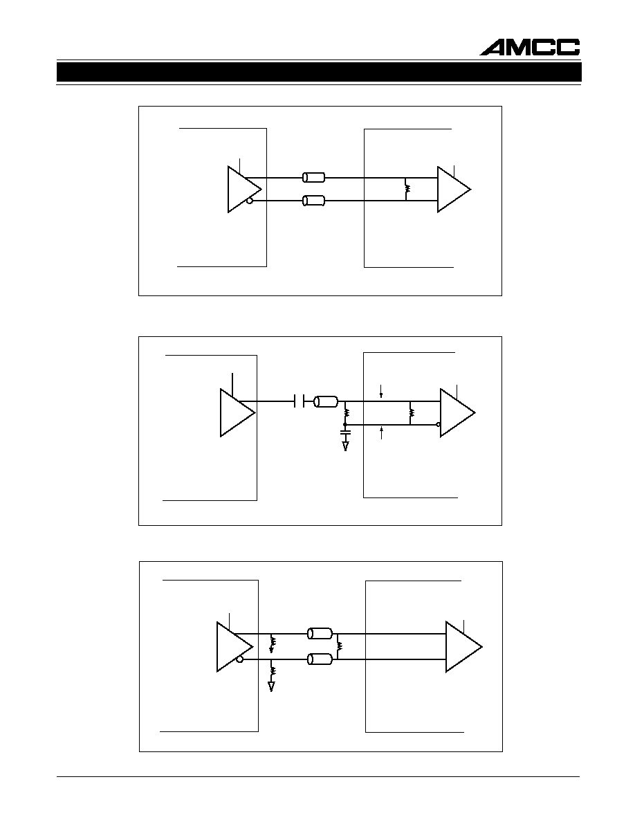
19
S3044
SONET/SDH/ATM OC-48 1:16 RECEIVER
November 22, 1999 / Revision F
+3.3V
S3044
LSDP/N
LSCLKP/N
+3.3V
100
S3043
LSDP/N
LSCLKP/N
Z
0
=50
Z
0
=50
Figure 20. S3043 to S3044 for Diagnostic Loopback
Figure 21. Single-Ended LVPECL Driver to S3044 Input
AC Coupled Termination
Vcc -0.70V
(DC AVG)
Vcc -0.70V
(DC AVG)
S3044
RSDP/N
RSCLKP/N
Vcc
300
.01
µ
F
.01
µ
F
+3.3V
60
Single-Ended
Driver
Z
0
=50
Figure 22. Differential LVPECL Termination
+3.3V
LVPECL
Differential Input
+3.3V
100
220
220
POCLKP/N
Z
0
=50
Z
0
=50

S3044
SONET/SDH/ATM OC-48 1:16 RECEIVER
20
November 22, 1999 / Revision F
X XXXX X
Prefix Device Package
S3044
SONET/SDH/ATM OC-48 1:16 RECEIVER
C
E
R T I F I E
D
IS
O 9001
AMCC is a registered trademark of Applied Micro Circuits Corporation.
Copyright Æ 1999 Applied Micro Circuits Corporation
AMCC reserves the right to make changes to its products or to discontinue any semiconductor product or service without notice, and
advises its customers to obtain the latest version of relevant information to verify, before placing orders, that the information being relied
on is current.
AMCC does not assume any liability arising out of the application or use of any product or circuit described herein, neither does it convey
any license under its patent rights nor the rights of others.
AMCC reserves the right to ship devices of higher grade in place of those of lower grade.
AMCC SEMICONDUCTOR PRODUCTS ARE NOT DESIGNED, INTENDED, AUTHORIZED, OR WARRANTED TO BE SUITABLE
FOR USE IN LIFE-SUPPORT APPLICATIONS, DEVICES OR SYSTEMS OR OTHER CRITICAL APPLICATIONS.
Applied Micro Circuits Corporation
6290 Sequence Drive, San Diego, CA 92121
Phone: (858) 450-9333 ∑ (800) 755-2622 ∑ Fax: (858) 450-9885
http://www.amcc.com
X
I
F
E
R
P
E
C
I
V
E
D
E
G
A
K
C
A
P
t
i
u
c
r
i
C
d
e
t
a
r
g
e
t
n
I
≠
S
4
4
0
3
P
E
T
/
P
F
Q
P
0
8
≠
A
Ordering Information