Äîêóìåíòàöèÿ è îïèñàíèÿ www.docs.chipfind.ru

A49LF004
4 Mbit CMOS 3.3Volt-only Firmware Hub Flash Memory
Preliminary
PRELIMINARY (November, 2003, Version 0.0)
AMIC Technology, Corp.
Document Title
4 Mbit CMOS 3.3 Volt-only Firmware Hub Flash Memory
Revision History
Rev. No. History Issue
Date Remark
0.0
Initial issue
November 21, 2003
Preliminary

A49LF004
4 Mbit CMOS 3.3Volt-only Firmware Hub Flash Memory
Preliminary
PRELIMINARY (November, 2003, Version 0.0)
1
AMIC Technology, Corp.
FEATURES
· Single Power Supply Operation
-
Low voltage range: 3.0 V - 3.6 V for Read and Write
Operations
· Standard Intel Firmware Hub Interface
-
Read compatible to Intel® 82802 Firmware
Hub devices
· Memory Configuration
-
512K x 8 (4 Mbit)
· Block Architecture
-
4Mbit: eight uniform 64KByte blocks
-
Supports full chip erase for Address/Address
Multiplexed (A/A Mux) mode
·
Automatic Erase and Program Operation
-
Embedded Byte Program and Block/Chip Erase
algorithms
-
Typical 10 µs/byte programming time
-
Typical 1s block erase time
· Two Operational Modes
-
Firmware Hub Interface (FWH) Mode for in-system
operation
-
Address/Address Multiplexed (A/A Mux) Interface
Mode for programming equipment
· Firmware Hub (FWH) Mode
-
33 MHz synchronous operation with PCI bus
-
5-signal communication interface for in-system read
and write operations
-
Standard SDP Command Set
-
Data# Polling (I/O
7
) and Toggle Bit (I/O
6
) features
-
Block Locking Register for all blocks
-
4 ID pins for multi-chip selection
-
5 GPI pins for General Purpose Input Register
-
TBL# pin for hardware write protection to Boot Block
-
WP# pin for hardware write protection to whole
memory array except Boot Block
· Address/Address Multiplexed (A/A Mux) Mode
-
11-pin multiplexed address and 8-pin data I/O
interface
-
Supports fast programming on EPROM programmers
-
Standard SDP Command Set
-
Data# Polling (I/O
7
) and Toggle Bit (I/O
6
) features
· Lower Power Consumption
-
Typical 12mA active read current
-
Typical 24mA program/erase current
·
High Product Endurance
-
Guarantee 100,000 program/erase cycles for each
block
-
Minimum 20 years data retention
· Compatible Pin-out and Packaging
-
32-pin (8 mm x 14 mm) TSOP (TYPE I)
-
32-pin PLCC
GENERAL DESCRIPTION
The A49LF004 flash memory device is designed to be read-
compatible with the Intel 82802 Firmware Hub (FWH)
device for PC-BIOS application. This device is designed to
use a single low voltage, range from 3.0 Volt to 3.6 Volt
power supply to perform in-system or off-system read and
write operations. It provides protection for the storage and
update of code and data in addition to adding system
design flexibility through five general-purpose inputs. Two
interface modes are supported by the A49LF004: Firmware
Hub (FWH) Interface mode for In-System programming and
Address/Address Multiplexed (A/A Mux) mode for fast
factory programming of PC-BIOS applications.
The memory is divided into eight uniform 64Kbyte blocks
that can be erased independently without affecting the data
in other blocks. Blocks also can be protected individually to
prevent accidental Program or Erase commands from
modifying the memory. The Program and Erase operations
are executed by issuing the Program/Erase commands into
the command interface by which activating the internal
control logic to automatically process the Program/Erase
procedures. The device can be programmed on a byte-by-
byte basis after performing the Erase operation. In addition
to the Block Erase operation, the Chip Erase feature is
provided in A/A Mux mode that allows the whole memory to
be erased in one single Erase operation. The A49LF004
provides the status detection such as Data# Polling and
Toggle Bit Functions in both FWH and A/A Mux modes. The
process or completion of Program and Erase operations
can be detected by reading the status bits.
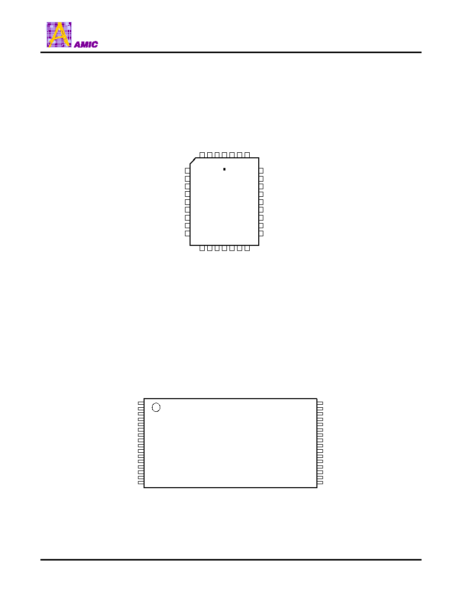
The A49LF004 is offered in 32-lead TSOP and 32-lead
PLCC packages. See Figures 1 and 2 for pin assignments
and Table 1 for pin descriptions.
A49LF004
PRELIMINARY (November, 2003, Version 0.0)
2
AMIC Technology, Corp.
PIN CONFIGURATIONS
A7 (FGPI1)
A6 (FGPI0)
A5 (WP#)
A4 (TBL#)
A3 (ID3)
A2 (ID2)
A1 (ID1)
A0 (ID0)
I/O
0
(FWH0)
21
22
23
24
25
26
27
28
29
12
13
11
8
9
5
7
6
RB# (RES)
I/O
7
(RES)
WE# (FWH4)
32-lead PLCC
Top View
OE# (INIT#)
VDD (VDD)
NC
NC
VSS (VSS)
IC (IC)
I/
O
1
(F
W
H
1
)
I/
O
2
(F
W
H
2
)
VS
S (
V
S
S
)
I/
O
3
(F
W
H
3
)
I/
O
4
(
R
ES)
I/
O
5
(
R
ES)
I/
O
6
(
R
ES)
4
3
2
1
32
31
30
A8
(
F
GPI
2
)
A
9
(
F
G
P
I3
)
RS
T#
(
R
S
T
#
)
NC
VD
D
(
V
DD
)
R/
C# (
C
L
K
)
A1
0 (
F
GP
I
4
)
14
15
16
17
18
19
20
10
(*) Designates FWH Mode
FIGURE 1: Pin Assignments for 32-Lead PLCC
32-lead TSOP (8
MM
X 14
MM
)
Top View
1
2
3
4
5
6
7
8
9
10
11
12
13
14
15
16
NC
NC
VSS (VSS)
IC (IC)
A10 (FGPI4)
R/C# (CLK)
VDD (VDD)
RST# (RST#)
A9 (FGPI3)
A8 (FGPI2)
A7 (FGPI1)
A6 (FGPI0)
A5 (WP#)
A4 (TBL#)
32
31
30
29
28
27
26
25
24
23
22
21
20
19
18
17
A3 (ID3)
A2 (ID2)
A1 (ID1)
A0 (ID0)
I/O
0
(FWH0)
I/O
1
(FWH1)
I/O
2
(FWH2)
VSS (VSS)
I/O
3
(FWH3)
I/O
4
(RES)
I/O
5
(RES)
I/O
6
(RES)
I/O
7
(RES)
VDD (VDD)
WE# (FWH4)
OE# (INIT#)
NC
NC
FIGURE 2: Pin Assignments for 32-Lead TSOP
(*) Designates FWH Mode
A49LF004
PRELIMINARY (November, 2003, Version 0.0)
3
AMIC Technology, Corp.
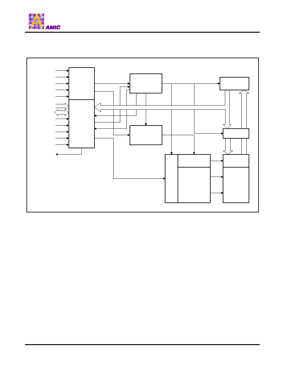
BLOCK DIAGRAM
High Voltage
Generator
Data Latch
FWH Mode
Interface
FWH[3:0]
CLK
FWH4
ID[3:0]
FGPI[4:0]
A/A Mux
Mode
Interface
A[10:0]
I/O
7
~ I/O
0
WE#
OE#
R/C#
IC
RST#
RB#
Addr
e
s
s
Lat
c
h
X-decoder
Y-Decoder
Cell Matrix
Y-Gating
Control Logic
Input/Output
Buffers
A49LF004
PRELIMINARY (November, 2003, Version 0.0)
4
AMIC Technology, Corp.
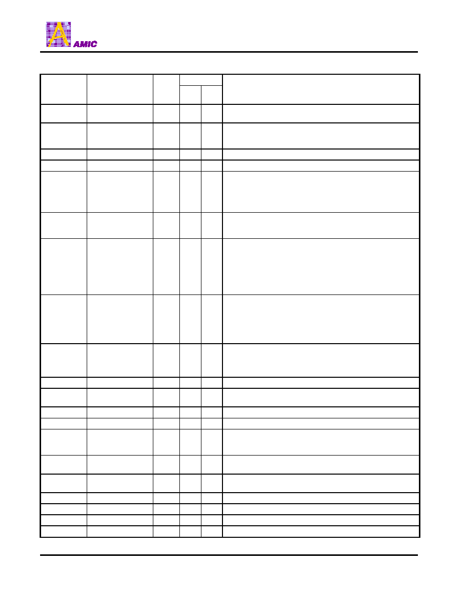
Table 1: Pin Description
1. IN=Input, OUT=output, I/O=Input/Output, PWR=Power
Interface
Symbol Pin
Name
Type
A/A
Mux
FWH
Descriptions
A
10
-A
0
Address
IN
X
Inputs for addresses during Read and Write operations in A/A
Mux mode. Row and column addresses are latched by R/C# pin.
I/O
7
-I/O
0
Data I/O
X
To output data during Read cycle and receive input data during
Write cycle in A/A Mux mode. The outputs are in tri-state when
OE# is high.
OE# Output
Enable
IN
X
To
control the data output buffers.
WE# Write
Enable
IN
X
To
control the Write operations.
IC
Interface
Configuration Pin
IN X X
To determine which interface is operational. When held high, A/A
Mux mode is enabled and when held low, FWH mode is enabled.
This pin must be setup at power-up or before return from reset
and not change during device operation. This pin is internally
pulled down with a resistor between 20-100 K
.
INIT# Initialize
IN
X
This is the second reset pin for in-system use. INIT# and RST#
pins are internally combined and initialize a device reset when
driven low.
ID[3:0] Identification
Inputs IN X
These four pins are part of the mechanism that allows multiple
FWH devices to be attached to the same bus. To identify the
component, the correct strapping of these pins must be set. The
boot device must have ID[3:0]=0000 and it is recommended that
all subsequent devices should use sequential up-count
strapping. These pins are internally pulled down with a resistor
between 20-100 K
.
FGPI[4:0]
General Purpose
Inputs
IN X
These individual inputs can be used for additional board
flexibility. The state of these pins can be read immediately at
boot, through FWH internal registers. These inputs should be at
their desired state before the start of the PCI clock cycle during
which the read is attempted, and should remain in place until the
end of the Read cycle. Unused FGPI pins must not be floated.
TBL#
Top Block Lock
IN
X
To prevent any write operations to the Boot Block when driven
low, regardless of the state of the block lock registers. When
TBL# is high it disables hardware write protection for the top
Boot Block. This pin cannot be left unconnected.
FWH[3:0]
FWH I/Os
I/O
X
I/O Communications in FWH mode.
CLK Clock
IN
X
To provide a clock input to the device. This pin is the same as
that for the PCI clock and adheres to the PCI specifications.
FWH4
FWH Input
IN
X
Input communication in FWH mode.
RST#
Reset
IN
X
X
To reset the operation of the device
WP# Write
Protect
IN
X
When low, prevents any write operations to all but the highest
addressable block. When WP# is high it disables hardware write
protection for these blocks. This pin cannot be left unconnected.
R/C# Row/Column
Select
IN X
This pin determines whether the address pins are pointing to the
row addresses or the column addresses in A/A Mux mode.
RB# Ready/Busy#
OUT
X
To determine if the device is busy in write operations. Valid only
in A/A Mux mode.
RES
Reserved
X
Reserved. These pins must be left unconnected.
VDD
Power Supply
PWR
X
X
To provide power supply (3.0-3.6Volt).
VSS
Ground
PWR
X
X
Circuit ground. All VSS pins must be grounded.
NC
No Connection
X
X
Unconnected pins.

A49LF004
PRELIMINARY (November, 2003, Version 0.0)
5
AMIC Technology, Corp.
ABSOLUTE MAXIMUM RATINGS*
Temperature Under Bias . . . . . . . . . . . . . -55
°C to + 125°C
Storage Temperature . . . . . . . . . . . . . . . . . -65
°C to + 125°C
D.C. Voltage on Any Pins with Respect to Ground
(1)
. . . . . . . . . . . . . . . . . . . . . . . . . . . . . . . -0.5V to VDD + 0.5V
Package Power Dissipation Capability (Ta=25
°C)
. . . . . . . . . . . . . . . . . . . . . . . . . . . . . . . -0.5V to VDD + 0.5V
Output Short Circuit Current
(2)
. . . . . . . . . . . . . . . . 50mA
Notes:
1. Minimum DC voltage on input or I/O pins is -0.5V. During
voltage transitions, input or I/O pins may undershoot VSS to -
2.0V for periods of up to 20ns. Maximum DC voltage on input
and I/O pins is VDD + 0.5V. During voltage transitions, input or
I/O pins may
overshoot to VDD + 2.0V for periods up to 20ns.
2. No more than one output is shorted at a time. Duration of the
short circuit should not be greater than one second.
*Comments
Stresses above those listed under "Absolute Maximum Ratings"
may cause permanent damage to this device. These are stress
ratings only. Functional operation of this device at these or any
other conditions above those indicated in the operational sections of
these specifications are not implied or intended. Exposure to the
absolute maximum rating conditions for extended periods may
affect device reliability.
Operating Ranges
Commercial (C) Devices
Ambient Temperature (T
A
) . . . . . . . . . . . . . . 0
°C to +85°C
VDD Supply Voltages
VDD for all devices . . . . . . . . . . . . . . . . . . +3.0V to +3.6V
Operating ranges define those limits between which the
functionally of the device is guaranteed.
MODE SELECTION
The A49LF004 flash memory devices can operate in two
distinct interface modes: the Firmware Hub Interface
(FWH) mode and the Address/Address Multiplexed (A/A
Mux) mode. The IC (Interface Configuration pin) is used to
set the interface mode selection. If the IC pin is set to logic
High, the device is in A/A Mux mode; while if the IC pin is set
Low, the device is in the FWH mode. The IC selection pin
must be configured prior to device operation. The IC pin is
internally pulled down if the pin is not connected. In FWH
mode, the device is configured to interface with its host
using Intel's Firmware Hub proprietary protocol.
Communication between Host and the A49LF004 occurs via
the 4-bit I/O communication signals, FWH [3:0] and the
FWH4. In A/A Mux mode, the device is programmed via an
11-bit address A
10
-A
0
and an 8-bit data I/O
7
-I/O
0
parallel
signals. The address inputs are multiplexed in row and
column selected by control signal R/C# pin. The column
addresses are mapped to the higher internal addresses, and
the row addresses are mapped to the lower internal
addresses. See the Device Memory Maps in Figure 3 for
address assignment.
FWH MODE OPERATION
The FWH interface consists of four data signals (FWH[3:0]),
one control signal (FWH4) and a clock (CLK). The data
signals, control signal and clock comply with PCI
specifications. Operations such as Memory Read and
Memory Write use Intel FWH propriety protocol. JEDEC
Standard SDP (Software Data Protection) Byte-Program and
Block-Erase command sequences are incorporated into the
FWH memory cycles. Chip-Erase command is only available
in A/A Mux mode. The addresses and data are transferred
through FWH[3:0] synchronized with the input clock CLK
during a FWH memory cycle. The pulse of FWH4 is inserted
for at least one clock period to indicate the start of a FWH
memory cycle. The address or data on FWH[3:0] is latched
on the rising edge of CLK. The device enters standby mode
when FWH4 is high and no internal operation is in progress.
The device is in ready mode when FWH4 is low and no
activity is on the FWH bus.
FWH Read Operation
FWH Read operations read from the memory cells or
specific registers in the FWH device. A valid FWH Read
operation starts when FWH4 is Low as CLK rises and a
START value "1101b" is on FWH[3:0]. Addresses and data
are transferred to and from the device decided by a series of
"fields". Field sequences and contents are strictly defined for
FWH Read operations. Refer to Table 2 for FWH Read
Cycle Definition.
FWH Write Operation
FWH Write operations write to the FWH Interface or FWH
registers. A valid FWH Write operation starts when FWH4 is
Low as CLK rises and a START value "1110b" is on
FWH[3:0]. Addresses and data are transferred to and from
the device decided by a series of "fields". Field sequences
and contents are strictly defined for FWH Write operations.
Refer to Table 3 for FWH write Cycle Definition.
FWH Abort Operation
If FWH4 is driven low for one or more clock cycles during a
FWH cycle, the cycle will be terminated and the device will
wait for the ABORT command. The host may drive the
FWH[3:0] with `1111b' (ABORT command) to return the
device to Ready mode. If abort occurs during a Write
operation, the data may be incorrectly altered.
Response To Invalid Fields
During FWH operations, the FWH will not explicitly indicate
that it has received invalid field sequences. The response to
specific invalid fields or sequences is as follows:
Address out of range:
The FWH address sequence is 7
fields long (28 bits), but only the last five address fields
(20 bits) will be decoded by A49LF004. Address A22 has the
special function of directing reads and writes to the flash
memory (A22=1) or to the register space (A22=0).
A49LF004
PRELIMINARY (November, 2003, Version 0.0)
6
AMIC Technology, Corp.
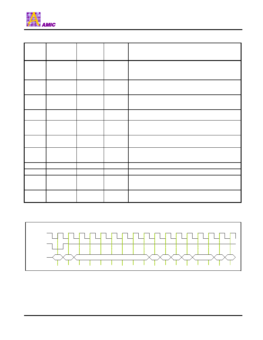
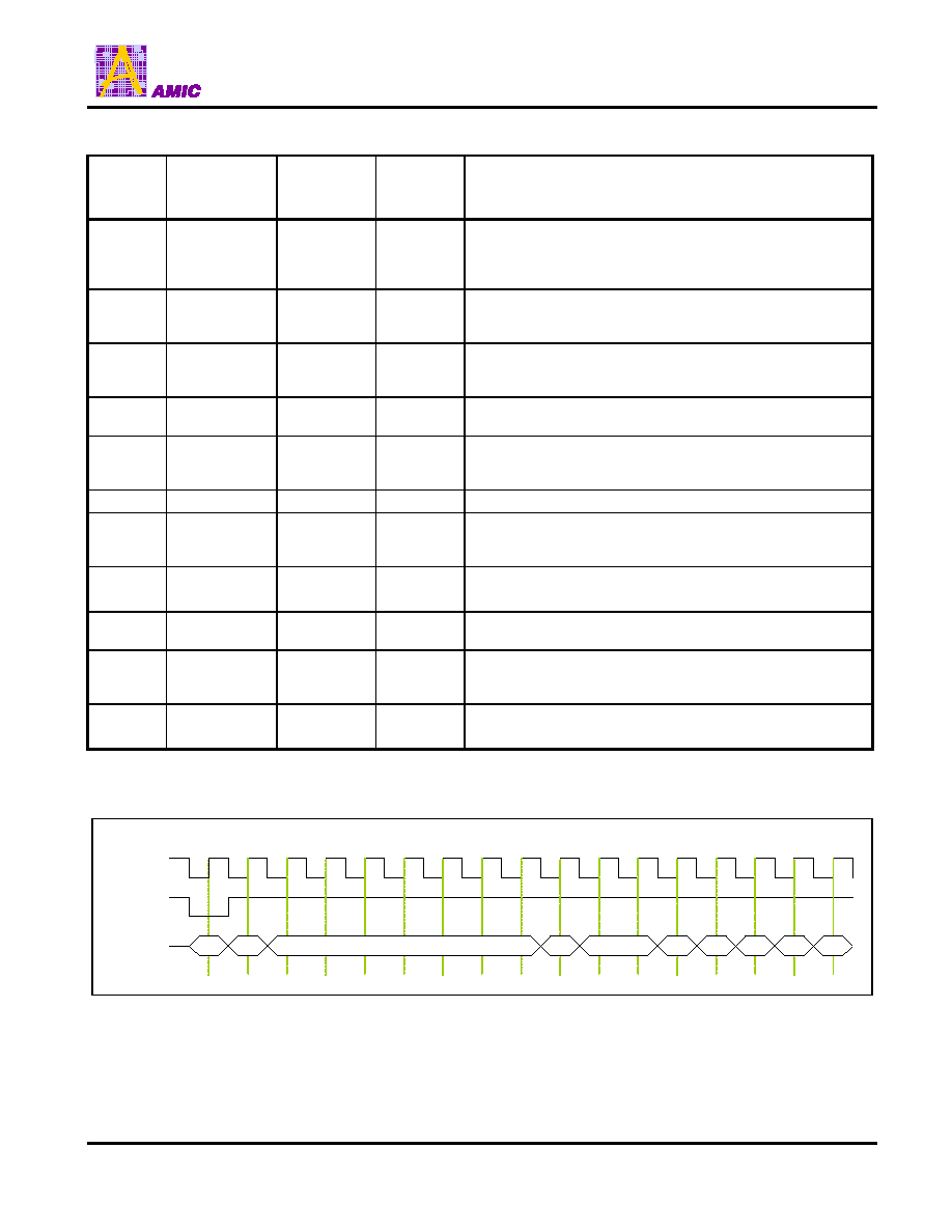
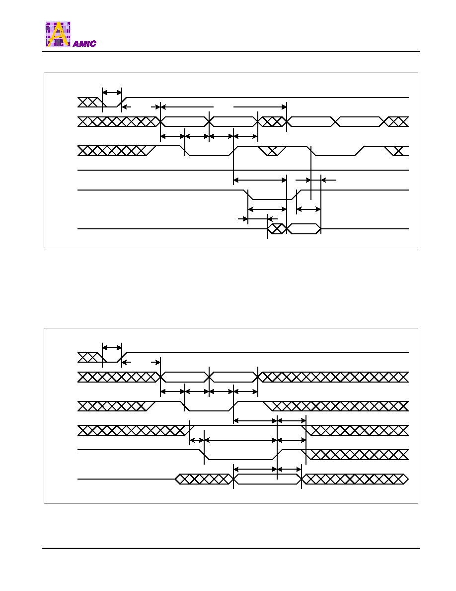
Table 2: FWH Read Cycle
FWH Single-Byte Read Waveforms
CLK
1
2
3
4
5
6
7
8
9
10
11
12
13
14
15
16
17
START
IDSEL
IMADDR
IMSIZE
TAR0
TAR1
RSYNC
DATA
TAR0
TAR1
FWH4
FWH[3:0]
Clock
Cycle
Field FWH[3:0]
MEMORY
I/O
Descriptions
1 START 1101 IN
FWH4 must be active (low) for the part to respond. Only the last
start field (before FWH4 transitioning high) should be
recognized. The START field contents indicate an FWH read
cycle.
2
IDSEL
0000 to 1111
IN
Indicates which FWH device should respond. If the IDSEL (ID
select) field matches the value ID[3:0], then that particular device
will respond to subsequent commands.
3-9 IMADDR YYYY IN
These seven clock cycles make up the 28-bit memory address.
YYYY is one nibble of the entire address. Addresses are
transferred most-significant nibble first.
10
IMSIZE
0000 (1 byte)
IN
A field of this size indicates how many bytes will be transferred
during multibyte operations.
11 TAR0 1111
IN
then float
In this clock cycle, the master (Intel ICH) has driven the bus to all
1s and then floats the bus, prior to the next clock cycle. This is
the first part of the bus "turnaround cycle."
12 TAR1
1111
(float)
Float
then OUT
The FWH takes control of the bus during this cycle. During the
next clock cycle, it will be driven "sync data."
13 RSYNC
0000
(READY)
OUT
During this clock cycle, the FWH will generate a "ready-sync"
(RSYNC) indicating that the least-significant nibble of the least-
significant byte will be available during the next clock cycle.
14
DATA
YYYY
OUT
YYYY is the least-significant nibble of the data byte.
15
DATA
YYYY
OUT
YYYY is the most-significant nibble of the data byte.
16 TAR0 1111
OUT
then float
In this clock cycle, the A49LF004 has driven the bus to all 1s and
then floats the bus prior to the next clock cycle. This is the first
part of the bus "turnaround cycle."
17 TAR1
1111
(float)
Float
then IN
The master (Intel ICH) resumes control of the bus during this
cycle.
A49LF004
PRELIMINARY (November, 2003, Version 0.0)
7
AMIC Technology, Corp.
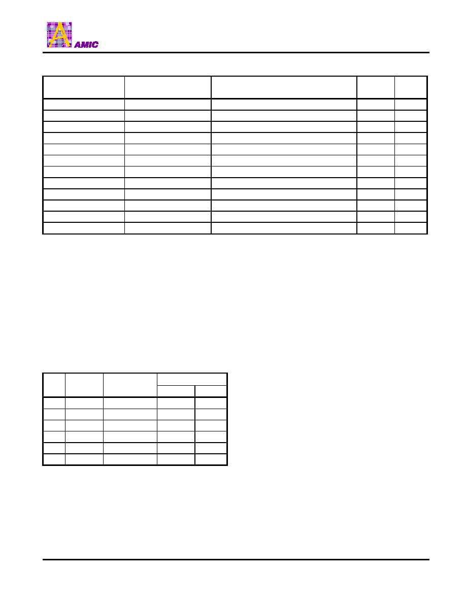
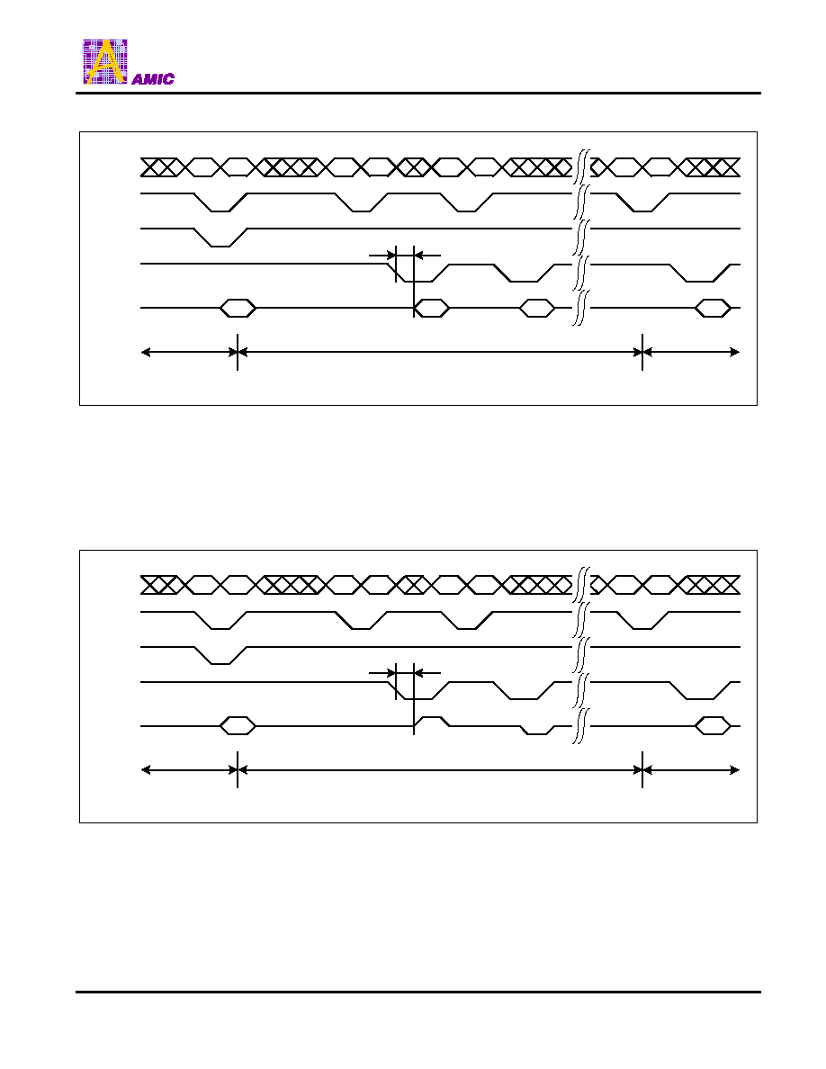
Table 3: FWH Write Cycle
FWH Write Waveforms
CLK
1
2
3
4
5
6
7
8
9
10
11
12
13
14
15
16
17
START
IDSEL
IMADDR
IMSIZE
TAR0
TAR1
RSYNC
DATA
TAR0
TAR1
FWH4
FWH[3:0]
Clock
Cycle
Field FWH[3:0]
MEMORY
I/O
Descriptions
1 START 1110 IN
FWH4 must be active (low) for the part to respond. Only the last
start field (before FWH4 transitioning high) should be
recognized. The START field contents indicate an FWH write
cycle.
2
IDSEL
0000 to 1111
IN
Indicates which FWH device should respond. If the IDSEL (ID
select) field matches the value ID[3:0], then that particular device
will respond to subsequent commands.
3-9 IMADDR YYYY IN
These seven clock cycles make up the 28-bit memory address.
YYYY is one nibble of the entire address. Addresses are
transferred most-significant nibble first.
10
IMSIZE
0000 (1 byte)
IN
A field of this size indicates how many bytes will be transferred
during multibyte operations.
11 DATA YYYY IN
This field is the least-significant nibble of the data byte. This data
is either the data to be programmed into the flash memory or any
valid flash command.
12
DATA
YYYY
IN
This field is the most-significant nibble of the data byte.
13 TAR0 1111
IN
then float
In this clock cycle, the master (Intel ICH) has driven the bus to all
1s then floats the bus, prior to the next clock cycle. This is the
first part of the bus "turnaround cycle."
14 TAR1
1111
(float)
Float
then OUT
The A49LF004 takes control of the bus during this cycle. During
the next clock cycle it will be driving the "sync" data.
15 RSYNC 0000 OUT
The A49LF004 outputs the values 0000, indicating that it has
received data or a flash command.
16 TAR0 1111
OUT
then float
In this clock cycle, the A49LF004 has driven the bus to all ones
and then floats the bus prior to the next clock cycle. This is the
first part of the bus "turnaround cycle."
17 TAR1
1111
(float)
Float
then IN
The master (Intel ICH) resumes control of the bus during this
cycle.

A49LF004
PRELIMINARY (November, 2003, Version 0.0)
8
AMIC Technology, Corp.
Invalid IMSIZE field:
If the FWH receives an invalid size
field during a Read or Write operation, the device will reset
and no operation will be attempted. The A49LF004 will not
generate any kind of response in this situation. Invalid size
fields for a Read/Write cycle are anything but 0000b.
Device Memory Hardware Write Protection
The Top Boot Lock (TBL#) and Write Protect (WP#) pins are
provided for hardware write protection of device memory in
the A49LF004. The TBL# pin is used to write protect the top
boot block (64 Kbytes) at the highest flash memory address
range for the A49LF004. WP# pin write protects the
remaining blocks in the flash memory. An active low signal
at the TBL# pin prevents Program and Erase operations of
the top boot block. When TBL# pin is held high, write
protection of the top boot block is then determined by the
Boot Block Locking register. The WP# pin serves the same
function for the remaining blocks of the device memory. The
TBL# and WP# pins write protection functions operate
independently of one another. Both TBL# and WP# pins
must be set to their required protection states prior to
starting a Program or Erase operation. A logic level change
occurring at the TBL# or WP# pin during a Program or Erase
operation could cause unpredictable results. TBL# and WP#
pins cannot be left unconnected. TBL# is internally ORed
with the top Boot Block Locking register. When TBL# is low,
the top Boot Block is hardware write protected regardless of
the state of the Write-Lock bit for the Boot Block Locking
register. Clearing the Write-Lock bit in the register when
TBL# is low will have no functional effect, even though the
register may indicate that the block is no longer locked. WP#
is internally ORed with the Block Locking register. When
WP# is low, the blocks are hardware write protected
regardless of the state of the Write-Lock bit for the
corresponding Block Locking registers. Clearing the Write-
Lock bit in any register when WP# is low will have no
functional effect, even though the register may indicate that
the block is no longer locked.
Reset
A V
IL
on INIT# or RST# pin initiates a device reset. INIT#
and RST# pins have the same function internally. It is
required to drive INIT# or RST# pins low during a system
reset to ensure proper CPU initialization. During a Read
operation, driving INIT# or RST# pins low deselects the
device and places the output drivers, FWH[3:0], in a high-
impedance state. The reset signal must be held low for a
minimal duration of time T
RSTP
. A reset latency will occur if a
reset procedure is performed during a Program or Erase
operation. See Table 16, Reset Timing Parameters for more
information. A device reset during an active Program or
Erase will abort the operation and memory contents may
become invalid due to data being altered or corrupted from
an incomplete Erase or Program operation. In this case, the
device can take up to T
RSTE
to abort a Program or Erase
operation.
Write Operation Status Detection
The A49LF004 device provides two software means to
detect the completion of a Write (Program or Erase) cycle, in
order to optimize the system Write cycle time. The software
detection includes two status bits: Data# Polling (I/O
7
) and
Toggle Bit (I/O
6
). The End-of-Write detection mode is
incorporated into the FWH Read cycle. The actual
completion of the nonvolatile write is asynchronous with the
system; therefore, either a Data# Polling or Toggle Bit read
may be simultaneous with the completion of the Write cycle.
If this occurs, the system may possibly get an erroneous
result, i.e., valid data may appear to conflict with either I/O
7
or I/O
6
. In order to prevent spurious rejection, if an erroneous
result occurs, the software routine should include a loop to
read the accessed location an additional two times. If both
reads are valid, then the device has completed the Write
cycle, otherwise the rejection is valid.
Data# Polling (I/O
7
)
When the A49LF004 device is in the internal Program
operation, any attempt to read I/O
7
will produce the
complement of the true data. Once the Program operation is
completed, I/O
7
will produce true data. Note that even
though I/O
7
may have valid data immediately following the
completion of an internal Write operation, the remaining data
outputs may still be invalid: valid data on the entire data bus
will appear in subsequent successive Read cycles after an
interval of 1 µs. During internal Erase operation, any attempt
to read I/O
7
will produce a `0'. Once the internal Erase
operation is completed, I/O
7
will produce a `1'. Proper status
will not be given using Data# Polling if the address is in the
invalid range.
Toggle Bit (I/O
6
)
During the internal Program or Erase operation, any
consecutive attempts to read I/O
6
will produce alternating
`0's and `1's, i.e., toggling between 0 and 1. When the
internal Program or Erase operation is completed, the
toggling will stop.
Multiple Device Selection
The four ID pins, ID[3:0], allow multiple devices to be
attached to the same bus by using different ID strapping in a
system. When the A49LF004 is used as a boot device,
ID[3:0] must be strapped as 0000, all subsequent devices
should use a sequential up-count strapping (i.e. 0001, 0010,
0011, etc.). The A49LF004 will compare the strapping
values, if there is a mismatch, the device will ignore the
remainder of the cycle and go into standby mode. For further
information regarding FWH device mapping and paging,
please refer to the Intel 82801(ICH) I/O Controller Hub
documentation. Since there is no ID support in A/A Mux
mode, to program multiple devices a stand-alone PROM
programmer is recommended.
REGISTERS
There are three types of registers available on the
A49LF004, the General Purpose Inputs Register, Block
Locking Registers, and the JEDEC ID Registers. These
registers appear at their respective address location in the 4
GByte system memory map. Unused register locations will
read as 00H. Any attempt to read or write any register during
an internal Write operation will be ignored. Refer to Table 4
for the FWH register memory map.
A49LF004
PRELIMINARY (November, 2003, Version 0.0)
9
AMIC Technology, Corp.
Table 4: FWH Register Memory Map
General Purpose Inputs Register
The GPI_REG (General Purpose Inputs Register) passes
the state of FGPI[4:0] pins at power-up on the A49LF004. It
is recommended that the FGPI[4:0] pins are in the desired
state before FWH4 is brought low for the beginning of the
bus cycle, and remain in that state until the end of the cycle.
There is no default value since this is a pass-through
register. The GPI register for the boot device appears at
FFBC0100H in the 4 GByte system memory map, and will
appear elsewhere if the device is not the boot device.
Register is not available for read when the device is in
Erase/Program operation. See Table 5
for the GPI_REG bits
and function.
Table 5: General Purpose Inputs Register
Block Locking Registers
A49LF004 provides software controlled lock protection
through a set of Block Locking registers. The Block Locking
Registers are read/write registers and it is accessible
through standard addressable memory locations specified in
Table 6. Unused register locations will read as 00H.
Write-Lock.
The Write-Lock Bit determines whether the
contents of the Block can be modified (using the Program or
Erase Command). When the Write-Lock Bit is set to `1', the
block is write protected; any operations that attempt to
change the data in the block will fail and the Status Register
will report the error. When the Write-Lock Bit is reset to `0',
the block is not write protected through the Locking Register
and may be modified unless write protected through some
other means. If Top Block Lock, TBL#, is Low, V
IL
, then the
Top Block (Block 7) is write protected and cannot be
modified.
Similarly, if Write Protect, WP#, is Low, V
IL
, then the Main
Blocks (Blocks 0 to 6) are write protected and cannot be
modified. After power-up or reset the Write-Lock Bit is
always set to `1' (write protected).
Read-Lock.
The Read-Lock bit determines whether the
contents of the Block can be read (from Read mode). When
the Read-Lock Bit is set to `1', the block is read protected;
any operation that attempts to read the contents of the block
will
read 00h instead. When the Read-Lock Bit is reset to `0',
read
operations in the Block return the data programmed into the
block as expected. After power-up or reset the Read-Lock
Bit is always reset to `0' (not read protected).
Lock-Down.
The Lock-Down Bit provides a mechanism for
protecting software data from simple hacking and malicious
attack. When the Lock-Down Bit is set to `1', further
modification to the Write-Lock, Read-Lock and Lock-Down
Bits cannot be performed. A reset or power-up is required
before changes to these bits can be made. When the Lock-
Down Bit is reset to `0', the Write-Lock, Read-Lock and
Lock-Down Bits can be changed.
Memory
Address
Mnemonic Register
Name
Default
Type
FFBF0002h
T_BLOCK_LK
Top Block Lock Register (Block 7)
01h
R/W
FFBE0002h
T_MINUS01_LK
Top Block [-1] Lock Register (Block 6)
01h
R/W
FFBD0002h
T_MINUS02_LK
Top Block [-2] Lock Register (Block 5)
01h
R/W
FFBC0002h
T_MINUS03_LK
Top Block [-3] Lock Register (Block 4)
01h
R/W
FFBB0002h
T_MINUS04_LK
Top Block [-4] Lock Register (Block 3)
01h
R/W
FFBA0002h
T_MINUS05_LK
Top Block [-5] Lock Register (Block 2)
01h
R/W
FFB90002h
T_MINUS06_LK
Top Block [-6] Lock Register (Block 1)
01h
R/W
FFB80002h
T_MINUS07_LK
Top Block [-7] Lock Register (Block 0)
01h
R/W
FFBC0100h FGPI_REG
FWH
General
Purpose Input Register
N/A
R
FFBC0000h
MANUF_REG
Manufacturer ID Register
37h
R
FFBC0001h
DEV_REG
Device ID Register
95h
R
FFBC0003h CONT_REG
Continuation ID Register
7Fh
R
Pin Number
Bit
Bit
Name
Function
32-PLCC 32-TSOP
7:5 - Reserved -
-
4
FGPI[4]
GPI_REG Bit 4
30
6
3
FGPI[3]
GPI_REG Bit 3
3
11
2
FGPI[2]
GPI_REG Bit 2
4
12
1
FGPI[1]
GPI_REG Bit 1
5
13
0
FGPI[0]
GPI_REG Bit 0
6
14
A49LF004
PRELIMINARY (November, 2003, Version 0.0)
10
AMIC Technology, Corp.
Table 6: Lock Register Bit Definition
ADDRESS/ADDRESS MULTIPLEXED (A/A
MUX) MODE
Device Operation
Commands are used to initiate the memory operation
functions of the device. The data portion of the software
command sequence is latched on the rising edge of WE#.
During the software command sequence the row address is
latched on the falling edge of R/C# and the column address
is latched on the rising edge of R/C#. Refer to Table 7 and
Table 8 for operation modes and the command sequence.
Read
The Read operation of the A49LF004 device is controlled by
OE#. OE# is the output control and is used to gate data from
the output pins. Refer to the Read cycle timing diagram,
Figure 10 for further details.
Byte-Program Operation
The A49LF004 device is programmed on a byte-by-byte
basis. Before programming, one must ensure that the block,
in which the byte which is being programmed exists, is fully
erased. The Byte-Program operation is initiated by executing
a four-byte command load sequence for Software Data
Protection with address and data in the last byte sequence.
During the Byte-Program operation, the row address (A10-
A0) is latched on the falling edge of R/C# and the column
Address (A21-A11) is latched on the rising edge of R/C#.
The data bus is latched in the rising edge of WE#. See
Figure 11 for Program operation timing diagram, Figure 14
for timing waveforms, and Figure 19 for its flowchart. During
the Program operation, the only valid reads are Data#
Polling and Toggle Bit. During the internal Program
operation, the host is free to perform additional tasks. Any
commands written during the internal Program operation will
be ignored.
Reset
A V
IL
on RST# pin initiates a device reset.
Data
Reserved
Bit 7:3
Read-Lock
Bit 2
Lock-Down
Bit 1
Write-Lock
Bit 0
Function
00h 00000 0
0
0 Full
Access.
01h
00000
0
0
1
Write locked. Default state at power-up.
02h
00000
0
1
0
Locked open (full access locked down).
03h 00000 0
1
1 Write-locked
down.
04h 00000 1
0
0 Read
locked.
05h
00000
1
0
1
Read and Write locked.
06h 00000 1
1
0 Read-locked
down
07h
00000
1
1
1
Read- and Write-locked down
Data Function
7:3
Reserved
2
Read-Lock
1 = Prevents read operations in the block where set
0 = Normal operation for reads in the block where clear. This is the default state.
1
Lock-Down
1 = Prevents further set or clear operations to the Write-Lock and Read-Lock bits. Lock-Down only can be set
but not clear. The block will remain lock-down until reset (with RST# or INIT# being Low), or until the device
is power-on reset.
0 = Normal operation for Write-Lock and Read-Lock bit altering in the block where clear. This is the default state.
0
Write-Lock
1 = Prevents program or erase operations in the block where set. This is the default state.
0 = Normal operation for programming and erase in the block where clear.
A49LF004
PRELIMINARY (November, 2003, Version 0.0)
11
AMIC Technology, Corp.
Table 7: A/A Mux Mode Operation Selection
Block-Erase Operation
The Block-Erase Operation allows the system to erase the
device in 64 KByte uniform block size for the A49LF004. The
Block-Erase operation is initiated by executing a six-byte
command load sequence for Software Data Protection with
Block-Erase command (30H or 50H) and block address. The
internal Block-Erase operation begins after the sixth WE# pulse.
The End-of-Erase can be determined using either Data# Polling
or Toggle Bit methods. See Figure 15 for timing waveforms.
Any commands written during the Block- Erase operation will
be ignored.
Chip-Erase
The A49LF004 device provides a Chip-Erase operation only in
A/A Mux mode, which allows the user to erase the entire
memory array to the `1's state. This is useful when the entire
device must be quickly erased. The Chip-Erase operation is
initiated by executing a six-byte Software Data Protection
command sequence with Chip-Erase command (10H) with
address 5555H in the last byte sequence. The internal Erase
operation begins with the rising edge of the sixth WE#. During
the internal Erase operation, the only valid read is Toggle Bit or
Data# Polling. See Table 8 for the command sequence, Figure
16 for timing diagram, and Figure 21 for the flowchart. Any
commands written during the Chip-Erase operation will be
ignored.
Write Operation Status Detection
The A49LF004 device provides two software means to detect
the completion of a Write (Program or Erase) cycle, in
order to optimize the system Write cycle time. The software
detection includes two status bits: Data# Polling (I/O
7
) and
Toggle Bit (I/O
6
). The End-of-Write detection mode is enabled
after the rising edge of WE# which initiates the internal Program
or Erase operation. The actual completion of the nonvolatile
write is asynchronous with the system; therefore, either a Data#
Polling or Toggle Bit read may be simultaneous with the
completion of the Write cycle. If this occurs, the system may
possibly get an erroneous result, i.e., valid data may appear to
conflict with either I/O
7
or I/O
6
. In order to prevent spurious
rejection, if an erroneous result occurs, the software routine
should include a loop to read the accessed location an
additional two times. If both reads are valid, then the device has
completed the Write cycle, otherwise the rejection is valid.
Data# Polling (I/O
7
)
When the A49LF004 device is in the internal Program operation,
any attempt to read I/O
7
will produce the complement of the
true data. Once the Program operation is completed, I/O
7
will
produce true data. Note that even though I/O
7
may have valid
data immediately following the completion of an internal Write
operation, the remaining data outputs may still be invalid: valid
data on the entire data bus will appear in subsequent
successive Read cycles after an interval of 1 µs. During internal
Erase operation, any attempt to read I/O
7
will produce a `0'.
Once the internal Erase operation is completed, I/O
7
will
produce a `1'. The Data# Polling is valid after the rising edge of
fourth WE# pulse for Program operation. For Block- or Chip-
Erase, the Data# Polling is valid after the rising edge of sixth
WE# pulse. See Figure 12 for Data# Polling timing diagram.
Proper status will not be given using Data# Polling if the
address is in the invalid range.
Toggle Bit (I/O
6
)
During the internal Program or Erase operation, any
consecutive attempts to read I/O
6
will produce alternating `0's
and `1's, i.e., toggling between 0 and 1. When the internal
Program or Erase operation is completed, the toggling will stop.
The device is then ready for the next operation. The Toggle Bit
is valid after the rising edge of fourth WE# pulse for Program
operation. For Block- or Chip-Erase, the Toggle Bit is valid after
the rising edge of sixth WE# pulse. See Figure 13 for Toggle Bit
timing diagram.
Data Protection
The A49LF004 device provides both hardware and software
features to protect nonvolatile data from inadvertent writes.
Hardware Data Protection
Noise/Glitch Protection: A WE# pulse of less than 5 ns will not
initiate a Write cycle.
V
DD
Power Up/Down Detection: The Write operation is inhibited
when V
DD
is less than 1.5V.
Write Inhibit Mode: Forcing OE# low, WE# high will inhibit the
Write operation. This prevents inadvertent writes during power-
up or power-down.
Mode RST#
OE#
WE#
Address
I/O
Read V
IH
V
IL
V
IH
A
IN
D
OUT
Write V
IH
V
IH
V
IL
A
IN
D
IN
Standby V
IH
V
IH
V
IH
X
High
Z
Output Disable
V
IH
V
IH
X
X
High
Z
Reset V
IL
X X
X
High
Z
A21 A2 = X, A1 = V
IL
, A0 = V
IL
Manufacturer
ID
A21 A2 = X, A1 = V
IL
, A0 = V
IH
Device
ID
Product Identification
V
IH
V
IL
V
IH
A21 A2 = X, A1 = V
IH
, A0 = V
IH
Continuation
ID

A49LF004
PRELIMINARY (November, 2003, Version 0.0)
12
AMIC Technology, Corp.
Software Data Protection (SDP)
The A49LF004 provides the JEDEC approved Software
Data Protection scheme for all data alteration operation, i.e.,
Program and Erase. Any Program operation requires the
inclusion of a series of three-byte sequences. The three-byte
load sequence is used to initiate the Program operation,
providing optimal protection from inadvertent Write
operations, e.g., during the system power-up or power-down.
Any Erase operation requires the inclusion of a six-byte load
sequence. The A49LF004 device is shipped with the
Software Data Protection permanently enabled. See Table 8
for the specific software command codes. During SDP
command sequence, invalid commands will abort the device
to Read mode, within T
RC
.
Electrical Specifications
The AC and DC specifications for the FWH Interface signals
(FWH[3:0], CLK, FWH4, and RST#) as defined in Section
4.2.2 of the
PCI Local Bus Specification, Rev. 2.1
. Refer to
Table 9 for the DC voltage and current specifications. Refer
to the specifications on Table 10 to Table 19 for Clock,
Read/Write, and Reset operations.
Product Identification
The product identification mode identifies the Manufacturer
ID, Continuation ID, and Device ID of the A49LF004. See
Table 7 for detail information.
A49LF004
PRELIMINARY (November, 2003, Version 0.0)
13
AMIC Technology, Corp.
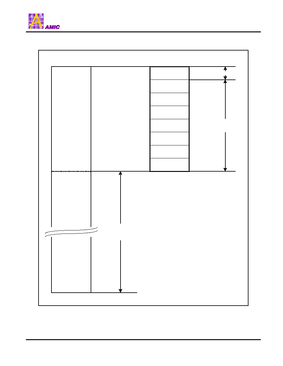
Figure 3: System Memory Map and Device Memory Map for A49LF004
System Memory
(Top 4M Bytes)
Block 7
(64K Bytes)
000000
00FFFF
010000
01FFFF
020000
02FFFF
030000
03FFFF
040000
04FFFF
050000
05FFFF
060000
06FFFF
070000
07FFFF
Block 6
(64K Bytes)
Block 5
(64K Bytes)
Block 4
(64K Bytes)
Block 3
(64K Bytes)
Block 2
(64K Bytes)
Block 1
(64K Bytes)
Block 0
(64K Bytes)
System Memory
(Top 4M Bytes)
TBL#
Device Memory
WP#
for Block 6 ~ 0
FFFFFFFFh
FFF80000h
FFC0000h
A49LF004
Range for
Additional FWH Devices
A49LF004
PRELIMINARY (November, 2003, Version 0.0)
14
AMIC Technology, Corp.
Table 8: Software Data Protection Command Definition
Notes:
1.
FWH Mode uses consecutive Write cycles to complete a command sequence; A/A Mux Mode uses consecutive bus cycles to complete a
command sequence.
2.
Addresses A14 A0 are used for SDP command decoding; A21 A15 can be V
IL
or V
IH
but no other value for the command sequence in
A/A Mux Mode.
3.
Chip erase is available in A/A Mux Mode only.
4.
BA: Block Erase Address.
5.
Either 30H or 50H are acceptable for Block Erase.
6.
PA: Program Byte Address; PD: Byte data to be programmed.
7.
Both Product ID Exit commands are equivalent.
1
st
Cycle
(1)
2
nd
Cycle
3
rd
Cycle
4
th
Cycle
5
th
Cycle
6
th
Cycle
Command
Bus
Cycles
Addr
(2)
Data Addr
Data
Addr
Data
Addr
Data Addr Data
Addr
Data
Block Erase
6
5555H AAH 2AAAH
55H
5555H
80H
5555H
AAH 2AAAH 55H
BA
(4)
30H/50H
(5)
Chip Erase
(3)
6
5555H AAH 2AAAH
55H
5555H
80H
5555H
AAH 2AAAH 55H
5555H
10H
Byte Program
4 5555H
AAH
2AAAH
55H
5555H
A0H
PA
(6)
PD
(6)
Product ID Entry
3 5555H
AAH
2AAAH
55H
5555H
90H
Product ID Exit
(7)
1 XXXX
F0H
Product ID Exit
(7)
3 5555H
AAH
2AAAH
55H
5555H
F0H
A49LF004
PRELIMINARY (November, 2003, Version 0.0)
15
AMIC Technology, Corp.
Operating Range
AC Conditions of Test
Table 9: DC Operating Characteristics (All Interfaces)
Notes:
1. I
DD
active while Erase or Program is in progress.
2.
The device is in Ready Mode when no activity is on the FWH bus.
3.
Do not violate processor or chipset specification regarding INIT# voltage.
Table 10: Recommended System Power-Up Timings
Symbol
Parameter Min
Units
T
PU-READ
(1)
Power-up to Read Operation
100
µs
T
PU-WRITE
(1)
Power-up to Write Operation
100
µs
Notes:
1.
This parameter is measured only for initial qualification and after a design or process change that could affect this parameter.
Range Ambient
Temperature
V
DD
Commercial 0
°C to +85°C 3.0-3.6V
Input Rise/Fall Time . . . . . . . . . . . . . . . . . . . . . . 3ns
Output Load . . . . . . . . . . . . . . . . . . . . . . . . . . . . CL = 30pF
Limits
Symbol
Parameter
Min Max
Units
Test Conditions
Active V
DD
Current:
Read
12
mA
I
DD
Active V
DD
Current:
Write
(1)
24
mA
Address Input=V
IL
/V
IH
, at F=1/T
RC
Min, V
DD
=V
DD
Max(A/A Mux
Mode)
OE#=V
IH
, WE#=V
IH
I
SB
Standby V
DD
Current
(FWH Mode)
100
µA
FWH4=0.9V
DD
,f=33MHz,V
DD
=V
DD
Max, All other inputs 0.9V
DD
or 0.1V
DD
I
RY
(2)
Ready Mode V
DD
Current
(FWH Mode)
10
mA
FWH4=V
IL
,f=33MHz,V
DD
=V
DD
Max, All other inputs 0.9V
DD
or
0.1V
DD
I
I
Input Current for IC and
ID[3:0] Pins
100
µA
V
IN
=GND to V
DD
, V
DD
=V
DD
Max
I
LI
Input Leakage Current
1
µA V
IN
=GND to V
DD
, V
DD
=V
DD
Max
I
LO
Output
Leakage
Current 1
µA V
OUT
=GND to V
DD
, V
DD
=V
DD
Max
V
IHI
(3)
INIT# Input High Voltage
1.0
V
DD
+0.5
V V
DD
=V
DD
Max
V
ILI
(3)
INIT# Input Low Voltage
-0.5
0.4
V
V
DD
=V
DD
Min
V
IH
Input High Voltage
0.5V
DD
V
DD
+0.5
V V
DD
=V
DD
Max
V
IL
Input Low Voltage
-0.5
0.3V
DD
V
V
DD
=V
DD
Min
V
OL
Output Low Voltage
0.1V
DD
V
IOL=1500
µA, V
DD
=V
DD
Min
V
OH
Output High Voltage
0.9V
DD
V
IOH=-500
µA, V
DD
=V
DD
Min
A49LF004
PRELIMINARY (November, 2003, Version 0.0)
16
AMIC Technology, Corp.
Table 11: Pin Impedance (V
DD
=3.3V, Ta=25
°C, f=1MHz, other pins open)
Parameter
Description Test
Condition
Max
C
I/O
(1)
I/O Pin Capacitance
V
I/O
= 0V
12pF
C
IN
(1)
Input Capacitance
V
IN
= 0V
12pF
L
PIN
(2)
Pin Inductance
20nH
Notes:
1.
This parameter is measured only for initial qualification and after a design or process change that could affect this parameter.
2.
Refer to PCI specifications.
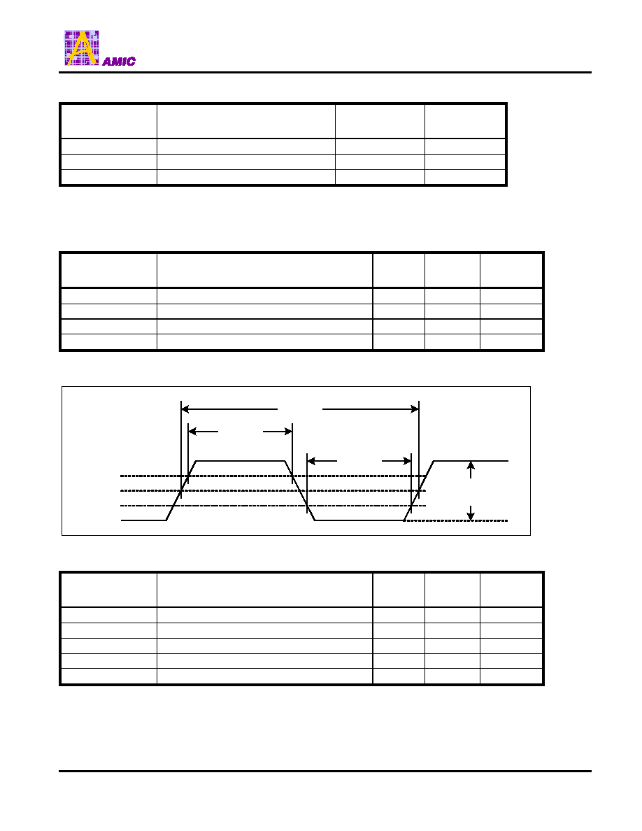
Table 12: Clock Timing Parameters
Symbol
Parameter Min
Max
Units
T
CYC
CLK Cycle Time
30
ns
T
HIGH
CLK High Time
11
ns
T
LOW
CLK Low Time
11
ns
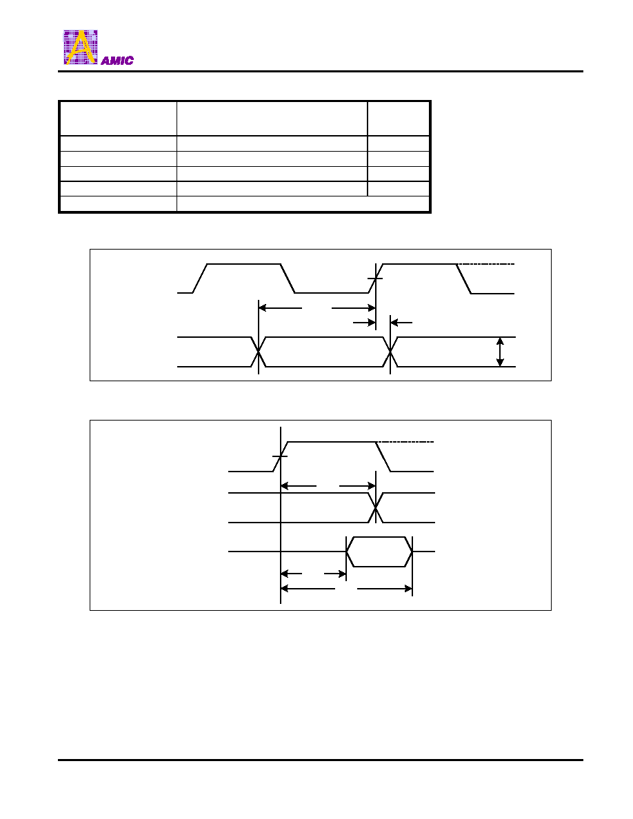
CLK Slew Rate (peak-to-peak)
1
4
V/ns
Figure 4: CLK Waveform
0.2 V
DD
0.5 V
DD
0.4 V
DD
0.3 V
DD
0.6 V
DD
0.4 V
DD
Peak-to-Peak
(Min)
T
CYC
T
LOW
T
HIGH
Table 13: FWH Mode Read/Write Cycle Timing Parameters, V
DD
=3.0-3.6V
Symbol
Parameter Min
Max
Units
T
SU
Input Set Up Time to CLK Rising
7
ns
T
DH
CLK Rising to Data Hold Time
0
ns
T
VAL
CLK Rising to Data Valid
2
11
ns
T
ON
CLK Rising to Active (Float to Active Delay)
2
ns
T
OFF
CLK Rising to Inactive (Active to Float Delay)
28
ns
A49LF004
PRELIMINARY (November, 2003, Version 0.0)
17
AMIC Technology, Corp.
Table 14: FWH Mode Interface Measurement Condition Parameters
Symbol
Value Units
V
TH
0.6 V
DD
V
V
TL
0.2 V
DD
V
V
TEST
0.4 V
DD
V
V
MAX
0.4 V
DD
V
Input Signal Edge Rate
1V/ns
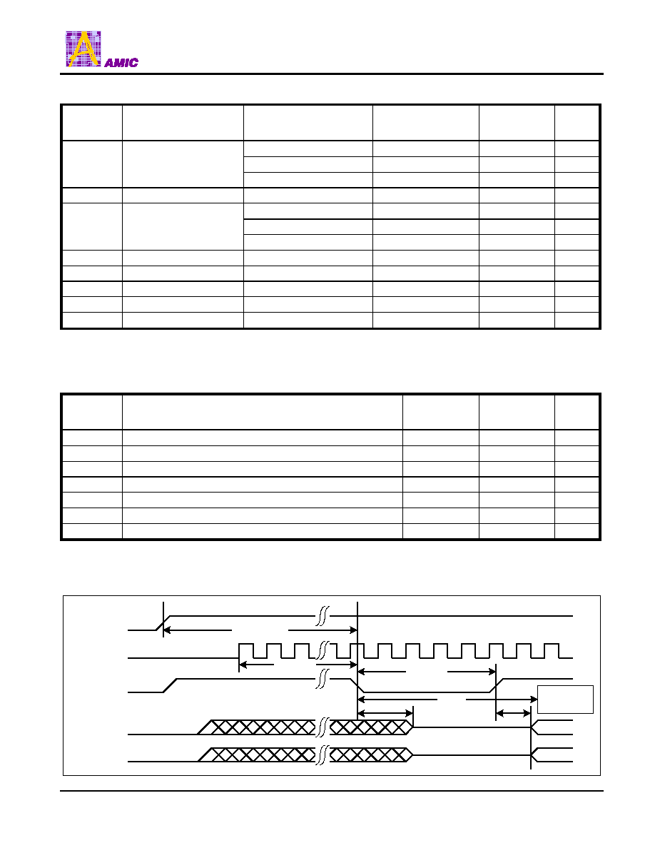
Figure 5: Input Timing Parameters
V
TL
V
TH
T
SU
V
TEST
CLK
FWH[3:0]
(Valid Input Data)
V
MAX
Valid Inputs
T
DH
Figure 6: Output Timing Parameters
V
TL
V
TH
T
ON
T
OFF
T
VAL
V
TEST
CLK
FWH[3:0]
(Valid Output Data)
FWH[3:0]
(Float Output Data)
A49LF004
PRELIMINARY (November, 2003, Version 0.0)
18
AMIC Technology, Corp.
Table 15: FWH Mode Interface AC Input/Output Characteristics
Symbol
Parameter Test
Conditions
Min Max
Units
0 < V
OUT
0.3V
DD
-12
V
DD
mA
0.3V
DD
< V
OUT
0.9V
DD
-17.1(V
DD
-V
OUT
)
mA
I
OH
(AC)
Switching Current High
0.7V
DD
< V
OUT
V
DD
Equation
C
mA
(Test Point)
V
OUT
= 0.7V
DD
-32
V
DD
mA
V
DD
> V
OUT
0.6V
DD
16V
DD
mA
0.6V
DD
> V
OUT
> 0.1V
DD
26.7V
OUT
mA
I
OL
(AC)
Switching Current Low
0.18V
DD
> V
OUT
> 0
Equation D
mA
(Test Point)
V
OUT
=0.18V
DD
38V
DD
mA
I
CL
Low Clamp Current
-3 < V
IN
-1
-25+(V
IN
+1)/0.015 mA
I
CH
High Clamp Current
V
DD
+4 > V
IN
> V
DD
+1 25+(V
IN
-V
DD
-1)/0.015 mA
slewr
Output Rise Slew Rate
0.2V
DD
-0.6V
DD
load
1
4
V/ns
slewf
Output Fall Slew Rate
0.6V
DD
-0.2V
DD
load
1
4
V/ns
Notes:
1.
See PCI specification.
2.
PCI specification output load is used.
Table 16: FWH Mode Interface Reset Timing Parameters, V
DD
=3.0-3.6V
Symbol
Parameter Min
Max
Units
T
PRST
V
DD
Stable to Reset Low
1
ms
T
KRST
Clock Stable to Reset Low
100
µs
T
RSTP
RST# Pulse Width
100
ns
T
RSTF
RST# Low to Output Float
48
ns
T
RST
(1)
RST# High to FWH4 Low
1
µs
T
RSTE
RST# Low to Reset During Erase or Program
10
µs
RST# or INIT# Slew Rate
50
mV/ns
Notes:
1.
There will be a latency of T
RSTE
if a reset procedure is performed during a Program or Erase operation.
Figure 7: Reset Timing Diagram
T
KRST
T
PRST
T
RST
T
RSTF
T
RSTE
T
RSTP
Program or Erase
Operation Aborted
V
DD
CLK
RST#/INIT#
FWH[3:0]
FWH4
A49LF004
PRELIMINARY (November, 2003, Version 0.0)
19
AMIC Technology, Corp.
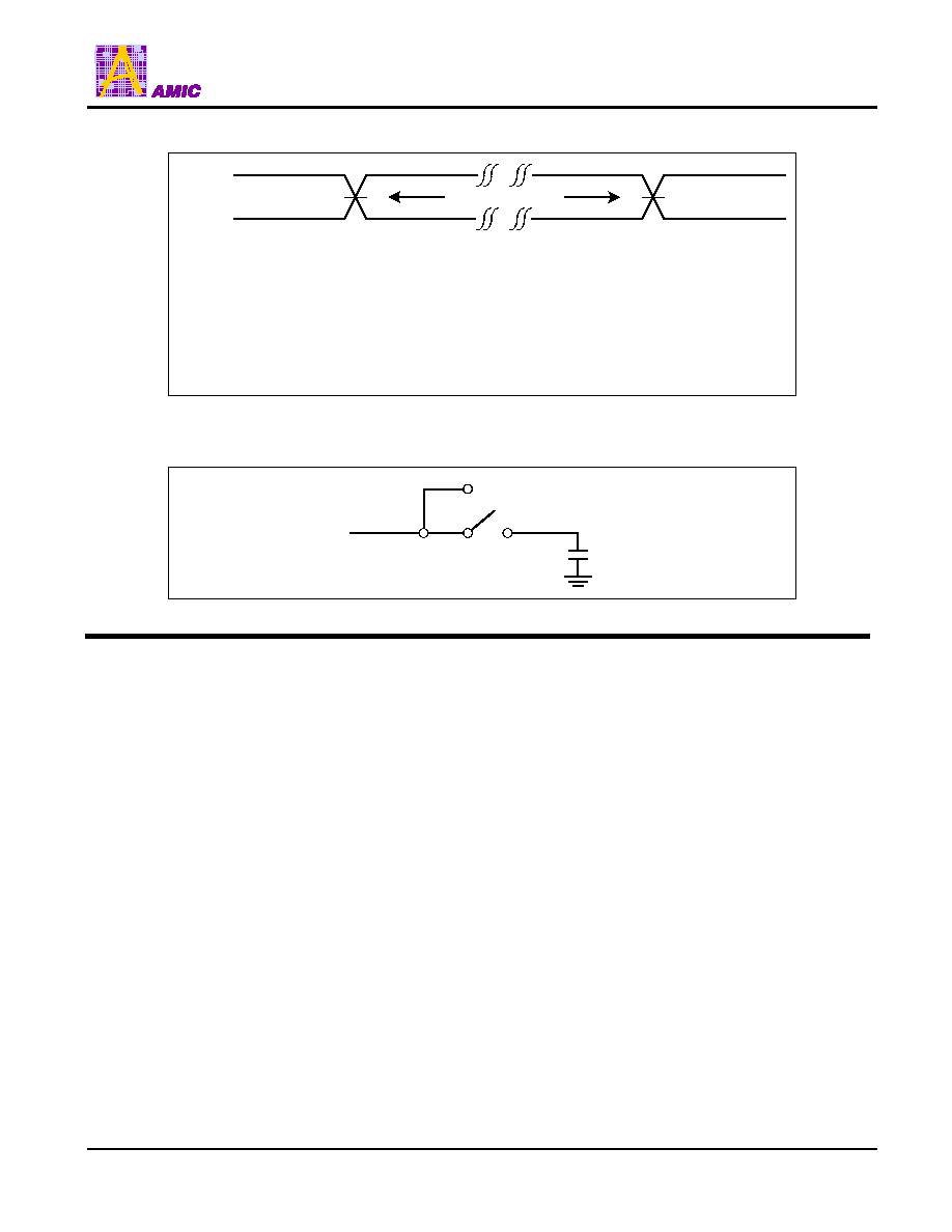
Figure 8: A/A Mux Mode AC Input/Output Reference Waveforms
V
IT
V
OT
Reference Points
INPUT
OUTPUT
V
IHT
V
ILT
AC test inputs are driven at V
IHT
(0.9V
DD
) for a logic HIGH and V
ILT
(0.1V
DD
) for a
logic LOW. Measurement reference points for inputs and outputs are V
IT
(0.5V
DD
)
and V
OT
(0.5V
DD
). Input rise and fall times (10% <-> 90%) are < 5ns
Note:
V
IT
: V
INPUT
Test
V
OT
: V
OUTPUT
Test
V
IHT
: V
INPUT
HIGH Test
V
ILT
: V
INPUT
LOW Test
Figure 9: A/A Mux Mode Test Load Condition
CL=30pF
TO TESTER
TO DUT
A49LF004
PRELIMINARY (November, 2003, Version 0.0)
20
AMIC Technology, Corp.
A/A MUX MODE AC CHARACTERISTICS
Table 17: Read Cycle Timing Parameters V
DD
=3.0-3.6V
Symbol
Parameter Min
Max
Units
T
RC
Read Cycle Time
270
ns
T
RST
RST# High to Row Address Setup
1
µs
T
AS
R/C# Address Set-up Time
45
ns
T
AH
R/C# Address Hold Time
45
ns
T
AA
Address Access Time
120
ns
T
OE
Output Enable Access Time
60
ns
T
OLZ
OE# Low to Active Output
0
ns
T
OHZ
OE# High to High-Z Output
35
ns
T
OH
Output Hold from Address Change
0
ns
Table 18: Program/Erase Cycle Timing Parameters, V
DD
=3.0-3.6V
Symbol
Parameter Min
Max
Units
T
RST
RST# High to Row Address Setup
1
µs
T
AS
R/C# Address Setup Time
50
ns
T
AH
R/C# Address Hold Time
50
ns
T
CWH
R/C# to Write Enable High Time
50
ns
T
OES
OE# High Setup Time
20
ns
T
OEH
OE# High Hold Time
20
ns
T
OEP
OE# to Data# Polling Delay
40
ns
T
OET
OE# to Toggle Bit Delay
40
ns
T
WP
WE# Pulse Width
100
ns
T
WPH
WE# Pulse Width High
100
ns
T
DS
Data Setup Time
50
ns
T
DH
Data Hold Time
5
ns
T
IDA
Product ID Access and Exit Time
150
ns
T
BP
Byte Programming Time
300
µs
T
BE
Block Erase Time
8
s
T
SCE
Chip Erase Time
10
s
Table 19: Reset Timing Parameters, V
DD
=3.0-3.6V
Symbol
Parameter Min
Max
Units
T
PRST
V
DD
Stable to Reset Low
1
ms
T
RSTP
RST# Pulse Width
100
ns
T
RSTF
RST# Low to Output Float
48
ns
T
RST
(1)
RST# High to FWH4 Low
1
µs
T
RSTE
RST# Low to Reset During Erase or Program
10
µs
1. There will be a reset latency of TRSTE if a reset procedure is performed during a Program or Erase operation.
A49LF004
PRELIMINARY (November, 2003, Version 0.0)
21
AMIC Technology, Corp.
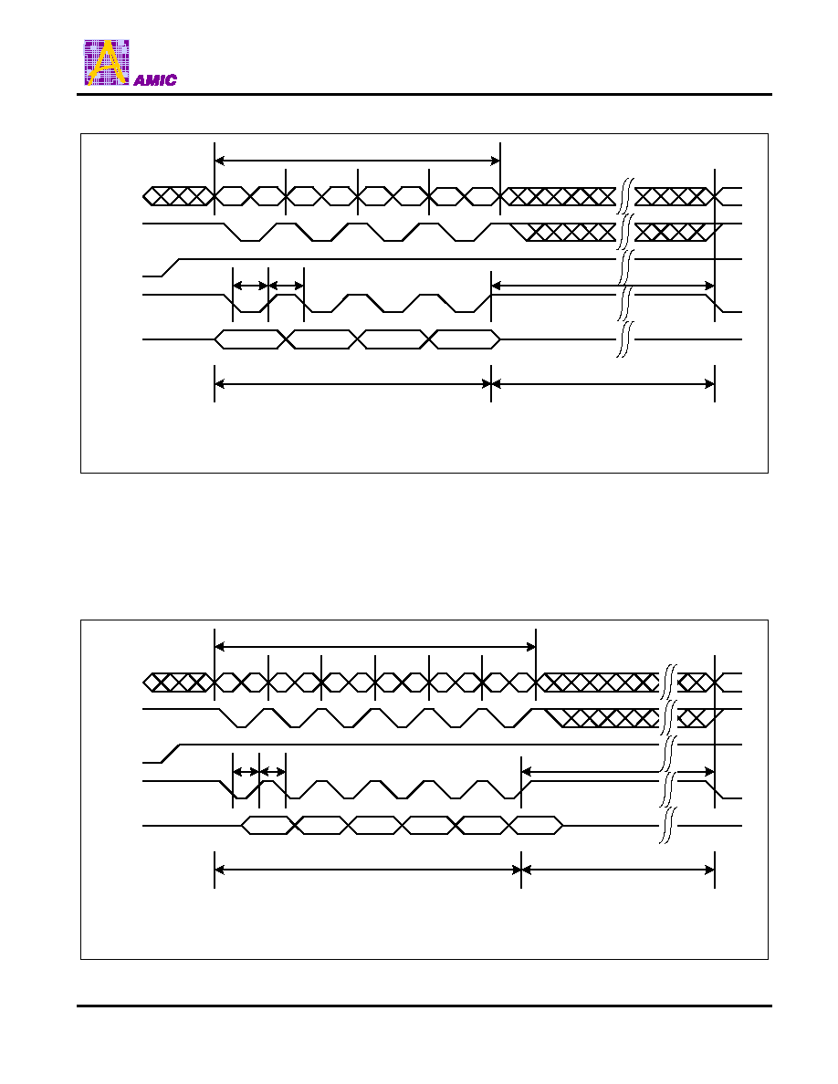
Figure 10: A/A Mux Mode Read Cycle Timing Diagram
T
RST
RST#
Address
WE#
OE#
I/O
7
-I/O
0
T
RSTP
Row Address
Column Address
Row Address
Column Address
T
RC
T
AS
T
AH
T
AS
T
AH
V
IH
T
OE
T
AA
T
OHZ
T
OH
T
OLZ
Data Valid
High-Z
High-Z
R/C#
Figure 11: A/A Mux Mode Write Cycle Timing Diagram
T
RST
RST#
Address
OE#
WE#
I/O
7
-I/O
0
T
RSTP
Row Address
Column Address
T
AS
T
AH
T
AS
T
AH
T
DS
T
WP
Data Valid
High-Z
R/C#
T
OES
T
WPH
T
DH
T
OEH
T
CWH
A49LF004
PRELIMINARY (November, 2003, Version 0.0)
22
AMIC Technology, Corp.
Figure 12: A/A Mux Mode Data# Polling Timing Diagram
Address
WE#
OE#
I/O
7
Row
Address
Column
Address
High-Z
R/C#
Write Operation
Complete
Data
In
Write Operation In
Progress
Final Input Command
Status Bit
Data
T
OEP
Command Input
Row
Address
Column
Address
Row
Address
Column
Address
Row
Address
Column
Address
Data#
Data#
Data
Status Bit
Figure 13: A/A Mux Mode Toggle Bit Timing Diagram
Address
WE#
OE#
I/O
6
Row
Address
Column
Address
High-Z
R/C#
Write Operation
Complete
Data
In
Write Operation In
Progress
Final Input Command
Status Bit
Data
T
OET
Command Input
Row
Address
Column
Address
Row
Address
Column
Address
Row
Address
Column
Address
Data
Status Bit
A49LF004
PRELIMINARY (November, 2003, Version 0.0)
23
AMIC Technology, Corp.
Figure 14: A/A Mux Mode Byte Program Timing Diagram
Address
OE#
WE#
I/O
7
-I/O
0
High-Z
R/C#
AA
Byte Program Operation In Progress
T
WP
Byte Program Command Input
55
A0
PD
T
WPH
T
BP
5555
2AAA
5555
PA
PA = Byte Program Address
PD = Byte Program Data
Four-Byte Byte Program Command Sequence
Figure 15: A/A Mux Mode Block Erase Timing Diagram
Address
OE#
WE#
I/O
7
-I/O
0
High-Z
R/C#
AA
Block Erase Operation In Progress
T
WP
Block Erase Command Input
T
WPH
5555
2AAA
5555
5555
BA = Block Address
Six-Byte Block Erase Command Sequence
55
80
AA
55
30/50
2AAA
BA
T
BE
A49LF004
PRELIMINARY (November, 2003, Version 0.0)
24
AMIC Technology, Corp.
Figure 16: A/A Mux Mode Chip Erase Timing Diagram
Address
OE#
WE#
I/O
7
-I/O
0
High-Z
R/C#
AA
Chip Erase Operation In Progress
T
WP
Chip Erase Command Input
T
WPH
5555
2AAA
5555
5555
Six-Byte Chip Erase Command Sequence
55
80
AA
55
10
2AAA
5555
T
SCE
Figure 17: A/A Mux Mode Product ID Entry and Read Timing Diagram
Address
OE#
WE#
I/O
7
-I/O
0
High-Z
R/C#
AA
T
WP
T
WPH
5555
2AAA
5555
Three-Byte Product ID Entry
Command Sequence
55
90
37
95
7F
0000
0001
0003
T
AA
T
IDA
Figure 18: A/A Mux Mode Product ID Exit and Reset Timing Diagram
Address
OE#
WE#
I/O
7
-I/O
0
High-Z
R/C#
AA
T
WP
T
WPH
5555
2AAA
5555
Three-Byte Product ID Exit and
Reset Command Sequence
55
F0
A49LF004
PRELIMINARY (November, 2003, Version 0.0)
25
AMIC Technology, Corp.
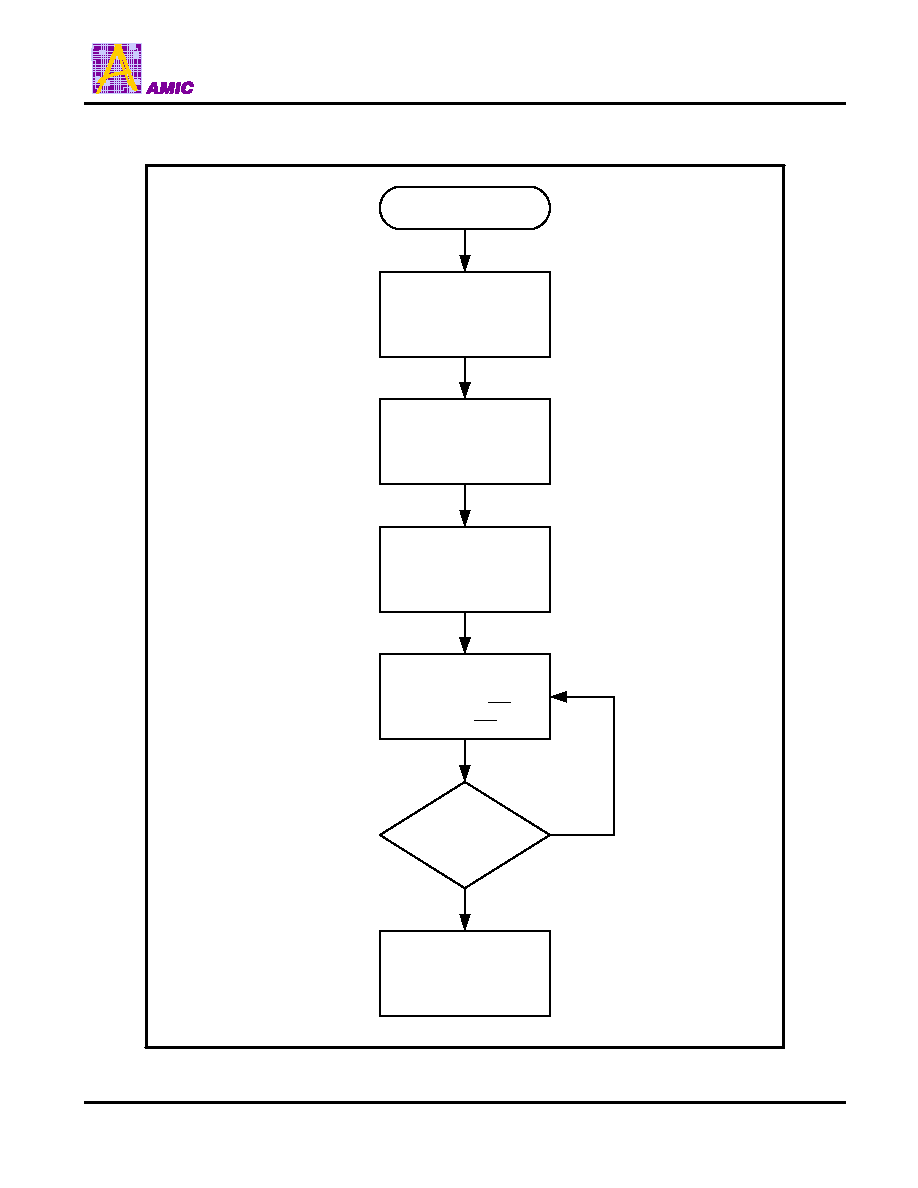
Figure 19: Automatic Byte Program Algorithm
Start
Write Command
Address: 5555H
Data: AAH
Write Command
Address: 2AAAH
Data: 55H
Write Command
Address: 5555H
Data: A0H
Write Command
Address: PA
Data: PD
I/O
7
= Data ?
Or
I/O
6
Stop Toggle?
Byte Program
Completed
NO
YES
PA: Byte Program Address
PD: Byte Program Data

A49LF004
PRELIMINARY (November, 2003, Version 0.0)
26
AMIC Technology, Corp.
Figure 20: Automatic Block Erase Algorithm
Start
Write Command
Address: 5555H
Data: AAH
Write Command
Address: 2AAAH
Data: 55H
Write Command
Address: 5555H
Data: 80H
Write Command
Address: 5555H
Data: AAH
I/O
7
= Data ?
Or
I/O
6
Stop Toggle?
Block Erase
Completed
NO
YES
BA: Block Address
Write Command
Address: 2AAAH
Data: 55H
Write Command
Address: BA
Data: 30H or 50H
A49LF004
PRELIMINARY (November, 2003, Version 0.0)
27
AMIC Technology, Corp.
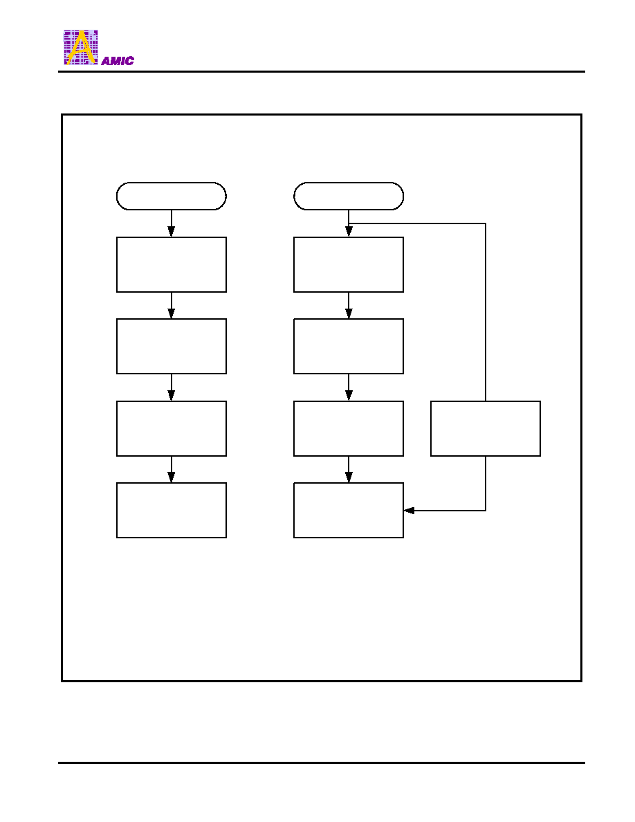
Figure 21: Automatic Chip Erase Algorithm
Start
Write Command
Address: 5555H
Data: AAH
Write Command
Address: 2AAAH
Data: 55H
Write Command
Address: 5555H
Data: 80H
Write Command
Address: 5555H
Data: AAH
I/O
7
= Data ?
Or
I/O
6
Stop Toggle?
Chip Erase
Completed
NO
YES
Write Command
Address: 2AAAH
Data: 55H
Write Command
Address: 5555H
Data: 10H
A49LF004
PRELIMINARY (November, 2003, Version 0.0)
28
AMIC Technology, Corp.
Figure 22: Product ID Command Flowchart
Start
Write Command
Address: 5555H
Data: AAH
Write Command
Address: 2AAAH
Data: 55H
Write Command
Address: 5555H
Data: 90H
Enter
Product ID Mode
Start
Write Command
Address: 5555H
Data: AAH
Write Command
Address: 2AAAH
Data: 55H
Write Command
Address: 5555H
Data: F0H
Exit
Product ID Mode
Write Command
Address: XXXXH
Data: F0H
OR
A49LF004
PRELIMINARY (November, 2003, Version 0.0)
29
AMIC Technology, Corp.
Ordering Information
A49LF004T x - 33 C
Temperature Range
C = Commercial (0
°
C to +85
°
C)
Clock Frequency
33 = 33MHz
Package Type
L = PLCC
X = TSOP (8mmX14mm)
Device Number
4 Mbit FWH Flash Memory
Part No.
Clock Frequency
(MHz)
Boot Block
Location
Temperature
Range
Package Type
A49LF004TL-33
33 Top
0
°C to +85°C
32-pin PLCC
A49LF004TX-33
33 Top
0
°C to +85°C
32-pin TSOP
(8mm X 14 mm)
A49LF004
PRELIMINARY (November, 2003, Version 0.0)
30
AMIC Technology, Corp.
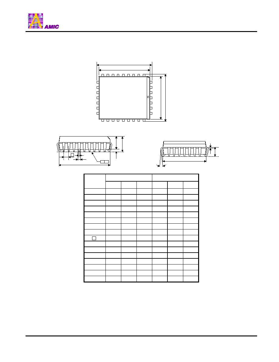
Package Information
PLCC 32L Outline Dimension
unit: inches/mm
A
1
A
2
A
e
D
y
H
D
D
13
G
D
b
1
b
G
E
c
5
14
20
21
29
30
32
1
4
E
H
E
L
Dimensions in inches
Dimensions in mm
Symbol
Min Nom
Max Min Nom
Max
A -
-
0.134
-
-
3.40
A
1
0.0185
- - 0.47
- -
A
2
0.105
0.110
0.115
2.67
2.80
2.93
b
1
0.026
0.028
0.032
0.66
0.71
0.81
b 0.016
0.018
0.021
0.41
0.46
0.54
C 0.008
0.010
0.014
0.20
0.254
0.35
D 0.547
0.550
0.553
13.89
13.97
14.05
E 0.447
0.450
0.453
11.35
11.43
11.51
e 0.044
0.050
0.056
1.12
1.27
1.42
G
D
0.490
0.510
0.530
12.45
12.95
13.46
G
E
0.390
0.410
0.430
9.91
10.41
10.92
H
D
0.585
0.590
0.595
14.86
14.99
15.11
H
E
0.485
0.490
0.495
12.32
12.45
12.57
L 0.075
0.090
0.095
1.91
2.29
2.41
y
- -
0.003
- -
0.075
0
° - 10°
0
° - 10°
Notes:
1. Dimensions D and E do not include resin fins.
2. Dimensions G
D
& G
E
are for PC Board surface mount pad pitch
design reference only.
A49LF004
PRELIMINARY (November, 2003, Version 0.0)
31
AMIC Technology, Corp.
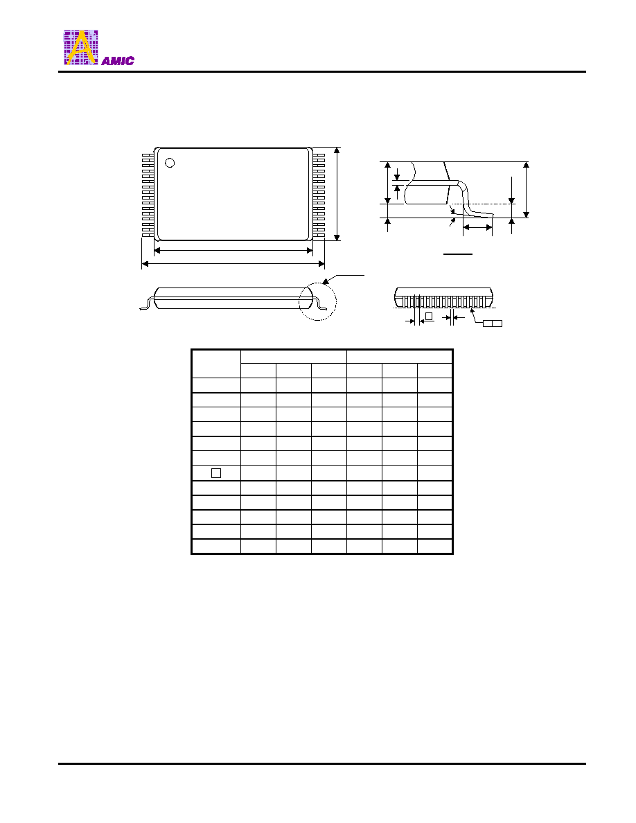
Package Information
TSOP 32L TYPE I (8 X 14mm) Outline Dimensions
unit: inches/mm
e
Detail "A"
Detail "A"
b
D
1
E
D
L
A
A
2
c
A
1
Pin1
Gage Plane
0.254
D y
Dimensions in inches
Dimensions in mm
Symbol
Min Nom
Max Min Nom
Max
A
- -
0.047
- -
1.20
A
1
0.002
- 0.006
0.05
- 0.15
A
2
0.037
0.039
0.041
0.95
1.00
1.05
b 0.0067
0.0087
0.0106
0.17
0.22
0.27
c 0.004
-
0.0083
0.10 - 0.21
E 0.311
0.315
0.319
7.90
8.00
8.10
e
- 0.0197
- - 0.50 -
D 0.543
0.551
0.559
13.80
14.00
14.20
D
1
0.484
0.488
0.492
12.30
12.40
12.50
L 0.020
0.024
0.028
0.50
0.60
0.70
y 0.000
- 0.003
0.00 - 0.076
0
°
3
°
5
°
0
°
3
°
5
°
Notes:
1. Dimension E does not include mold flash.
2. Dimension D
1
does not include interlead flash.
2. Dimension b does not include dambar protrusion.