Äîêóìåíòàöèÿ è îïèñàíèÿ www.docs.chipfind.ru
LP61L1008A
Preliminary
128K X 8 BIT 3.3V HIGH SPEED CENTER POWER CMOS SRAM
PRELIMINARY (August, 2001, Version 1.0)
1
AMIC Technology, Inc.
Features
n
Single 3.3V
±
10% power supply
n
Access times: 8/10/12 ns (max.)
n
Current: Operating: 160/155/150mA (max.)
Standby: 5mA (max.)
n
Full static operation, no clock or refreshing required
n
All inputs and outputs are directly TTL compatible
n
Center Power/Ground Pin Configuration
n
Common I/O using three-state output
n
Output enable and one chip enable inputs for easy
application
n
Data retention voltage: 2.0V (min.)
n
Available in 32-pin SOJ 300 mil package
General Description
The LP61L1008A is a high speed 1,048,576-bit static
random access memory organized as 131,072 words by
8 bits and operates on a single 3.3V power supply.
Inputs and three-state outputs are TTL compatible and
allow for direct interfacing with common system bus
structures.
The chip enable input is provided for POWER-DOWN
and device enable and an output enable input is included
for easy interfacing.
Data retention is guaranteed at a power supply voltage
as low as 2.0V.
Pin Configuration
A0
A1
A2
A3
CE
I/O
1
I/O
2
VCC
GND
I/O
3
I/O
4
WE
A4
A5
A6
A8
A7
A9
A10
A11
A12
I/O
5
I/O
6
VCC
I/O
7
I/O
8
OE
A13
A14
A15
A16
GND
LP61L1008AS
1
2
3
4
5
6
7
8
9
10
11
12
13
14
15
16
17
18
19
20
21
22
23
24
25
26
27
28
29
30
31
32
LP61L1008A
PRELIMINARY (August, 2001, Version 1.0)
2
AMIC Technology, Inc.
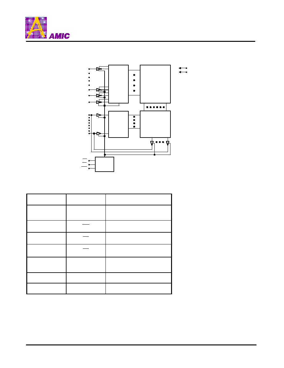
Block Diagram
DECODER
512 X 2048
MEMORY ARRAY
INPUT
DATA
CIRCUIT
COLUMN I/O
CONTROL
CIRCUIT
VCC
GND
A0
A14
A15
A16
I/O
1
I/O
8
CE
OE
WE
Pin Description
Pin No.
Symbol
Description
1 - 4, 13 - 21,
29- 32
A0 - A16
Address Inputs
12
WE
Write Enable
28
OE
Output Enable
5
CE
Chip Enable
6 7, 10 - 11,
22 23, 26 - 27
I/O
1
- I/O
8
Data Input/Outputs
8, 24
VCC
Power Supply
9, 25
GND
Ground
LP61L1008A
PRELIMINARY (August, 2001, Version 1.0)
3
AMIC Technology, Inc.
Recommended DC Operating Conditions
(T
A
= 0
°
C to + 70
°
C)
Symbol
Parameter
Min.
Typ.
Max.
Unit
VCC
Supply Voltage
3.0
3.3
3.6
V
GND
Ground
0
0
0
V
V
IH
Input High Voltage
2.2
-
VCC + 0.3
V
V
IL
Input Low Voltage
-0.3
0
+0.8
V
C
L
Output Load
-
-
30
pF
TTL
Output Load
-
-
1
-
Absolute Maximum Ratings*
VCC to GND .............................................. -0.5V to +4.6V
IN, IN/OUT Volt to GND .....................-0.5V to VCC +0.5V
Operating Temperature, Topr ...................... 0
°
C to +70
°
C
Storage Temperature, Tstg..................... -55
°
C to +125
°
C
Power Dissipation, Pt................................................1.0W
*Comments
Stresses above those listed under "Absolute Maximum
Ratings" may cause permanent damage to this device.
These are stress ratings only. Functional operation of
this device at these or any other conditions above
those indicated in the operational sections of this
specification is not implied or intended. Exposure to
the absolute maximum rating conditions for extended
periods may affect device reliability.
DC Electrical Characteristics
(T
A
= 0
°
C to + 70
°
C, VCC = 3.3V
±
10%, GND = 0V)
LP61L1008A- 8/10/12
Symbol
Parameter
Min.
Max.
Unit
Conditions
I
LI
Input Leakage Current
-
2
µ
A
V
IN
= GND to VCC
I
LO
Output Leakage Current
-
2
µ
A
CE = V
IH
or
OE = V
IH
or WE = V
IL
V
I/O
= GND to VCC
-8
-
160
-10
-
155
I
CC1
(1)
Dynamic Operating
Current
-12
-
150
mA
CE = V
IL
I
I/O
= 0 mA
I
SB
-
20
mA
CE = V
IH
I
SB1
Standby Power
Supply Current
-
5
mA
CE
VCC - 0.2V,
V
IN
0.2V or V
IN
VCC - 0.2V
V
OL
Output Low Voltage
-
0.4
V
I
OL
= 8 mA
V
OH
Output High Voltage
2.4
-
V
I
OH
= -4 mA
Note: 1. I
CC1
is dependent on output loading, cycle rates, and Read/Write patterns
LP61L1008A
PRELIMINARY (August, 2001, Version 1.0)
4
AMIC Technology, Inc.
Truth Table
Mode
CE
OE
WE
I/O Operation
Supply Current
Standby
H
X
X
High Z
I
SB
, I
SB1
Output Disable
L
H
H
High Z
I
CC1
Read
L
L
H
D
OUT
I
CC1
Write
L
X
L
D
IN
I
CC1
Note: X = H or L
Capacitance
(T
A
= 25
°
C, f = 1.0MHz)
Symbol
Parameter
Min.
Max.
Unit
Conditions
C
IN
*
Input Capacitance
6
pF
V
IN
= 0V
C
I/O
*
Input/Output Capacitance
8
pF
V
I/O
= 0V
* These parameters are sampled and not 100% tested.
AC Characteristics
(T
A
= 0
°
C to +70
°
C, VCC = 3.3V
±
10%, GND = 0V)
Symbol
Parameter
LP61L1008A-8 LP61L1008A-10
LP61L1008A-12
Unit
Min.
Max.
Min.
Max.
Min.
Max.
Read Cycle
t
RC
Read Cycle Time
8
-
10
-
12
-
ns
t
AA
Address Access Time
-
8
-
10
-
12
ns
t
ACE
Chip Enable Access Time
CE
-
8
-
10
-
12
ns
t
OE
Output Enable to Output Valid
-
4
-
5
-
6
ns
t
CLZ
Chip Enable to Output in Low Z
CE
3
-
3
-
5
-
ns
t
OLZ
Output Enable to Output in Low Z
0
-
0
-
2
-
ns
t
CHZ
Chip Disable to Output in High Z
CE
-
4
-
5
-
6
ns
t
OHZ
Output Disable to Output in High Z
0
4
0
5
2
6
ns
t
OH
Output Hold from Address Change
3
-
3
-
5
-
ns
LP61L1008A
PRELIMINARY (August, 2001, Version 1.0)
5
AMIC Technology, Inc.
AC Characteristics (continued)
Symbol
Parameter
LP61L1008A-8
LP61L1008A-10 LP61L1008A-12
Unit
Min.
Max.
Min.
Max.
Min.
Max.
Write Cycle
t
WC
Write Cycle Time
8
-
10
-
12
-
ns
t
CW
Chip Enable to End of Write
6
-
7
-
10
-
ns
t
AS
Address Setup Time of Write
0
-
0
-
0
-
ns
t
AW
Address Valid to End of Write
6
-
7
-
10
-
ns
t
WP
Write Pulse Width
6
-
7
-
8
-
ns
t
WR
Write Recovery Time
0
-
0
-
0
-
ns
t
WHZ
Write to Output in High Z
0
4
0
5
0
5
ns
t
DW
Data to Write Time Overlap
4
-
5
-
8
-
ns
t
DH
Data Hold from Write Time
0
-
0
-
0
-
ns
t
OW
Output Active from End of Write
3
-
3
-
5
-
ns
Notes: t
CHZ1
, t
CHZ2
, t
OHZ
, and t
WHZ
are defined as the time at which the outputs achieve the open circuit condition and are
not referred to output voltage levels.
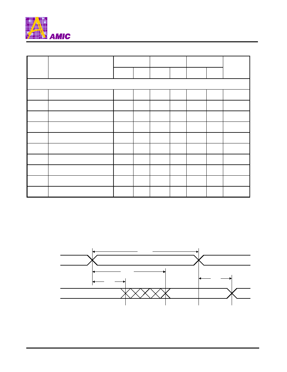
Timing Waveforms
Read Cycle 1
(1, 2, 4)
t
RC
t
OH
t
AA
t
OH
Address
D
OUT