 | –≠–ª–µ–∫—Ç—Ä–æ–Ω–Ω—ã–π –∫–æ–º–ø–æ–Ω–µ–Ω—Ç: AS1152 | –°–∫–∞—á–∞—Ç—å:  PDF PDF  ZIP ZIP |

AS1152
Quad LVDS Driver
austria
micro
systems
D a ta S h e e t
www.austriamicrosystems.com
Revision 1.00
1 - 15
1 General Description
The AS1152 is a Quad Flow-Through LVDS (Low-Volt-
age Differential Signaling) Line Driver which accepts
and converts LVTTL/LVCMOS input levels into LVDS
output signals. The device is perfect for low-power low-
noise applications requiring high signaling rates and
reduced EMI emissions.
The device is guaranteed to transmit data at speeds up
to 500Mbps (250MHz) over controlled impedance media
of approximately 100
. Supported transmission media
are PCB traces, backplanes, and cables.
The AS1152 is capable of setting all four outputs to a
high-impedance state through two Enable Inputs (EN
and ENn ≠ internally pulled down to GND), dropping the
device to an ultra-low-power state of 16mW (typical) dur-
ing high impedance. The Enable Inputs are common to
all four drivers.
Outputs conform to the ANSI TIA/EIA-644 LVDS stan-
dards. Flow-through pinout simplifies PC board layout
and reduces crosstalk by separating the LVTTL/LVC-
MOS inputs and LVDS outputs.
The AS1152 operates from a single +3.3V supply and is
specified for operation from -40 to +85∞C.
Figure 1. Block Diagram
2 Key Features
!
Flow-Through Pinout
!
Guaranteed 500Mbps Data Rate (paired with
AS1150)
!
350ps Pulse Skew (Max)
!
Conforms to ANSI TIA/EIA-644 LVDS Standards
!
Single +3.3V Supply
!
Operating Temperature Range: -40 to +85∞C
!
16-Pin TSSOP Package
3 Applications
Digital Copiers, Laser Printers, Cellular Phone Base Sta-
tions, Add/Drop Muxes, Digital Cross-Connects,
DSLAMs, Network Switches/Routers, Backplane Inter-
connect, Clock Distribution Computers, Intelligent Instru-
ments, Controllers, Critical Microprocessors and
Microcontrollers, Power Monitoring, and Portable/Bat-
tery-Powered Equipment.
IN1
IN2
IN3
IN4
AS1152
OUT1+
OUT1-
OUT2+
OUT2-
OUT3+
OUT3-
OUT4+
OUT4-
ENn
EN
V
CC

www.austriamicrosystems.com
Revision 1.00
2 - 15
AS1152
austria
micro
systems
Data Sheet
4 Absolute Maximum Ratings
Stresses beyond those listed in Table 1 may cause permanent damage to the device. These are stress ratings only,
and functional operation of the device at these or any other conditions beyond those indicated in the operational sec-
tions of the specifications is not implied. Exposure to absolute maximum rating conditions for extended periods may
affect device reliability.
Table 1. Absolute Maximum Ratings
Parameter
Limits
Units
Notes
V
CC
to GND
-0.3 to +5.0
V
INx, EN, ENn to GND
-0.3 to (V
CC
+ 0.3)
V
OUTx+, OUTx- to GND
-0.3 to +5
V
Short Circuit Duration (OUTx+,
OUTx-)
Continuous
Continuous Power Dissipation
(T
A
= +70∞C)
755
mW
Derate 9.4mW/∞C Above +70∞C
Storage Temperature Range
-65 to +150
∫C
Maximum Junction Temperature
+150
∫C
Operating Temperature Range
-40 to +85
∫C
Package Body Temperature
260
∫C
The reflow peak soldering temperature (body
temperature) specified is in compliance with IPC/
JEDEC J-STD-020C "Moisture/ Reflow Sensitivity
Classification for Non-Hermetic Solid State Surface
Mount Devices".
ESD Protection
±4
kV
Human Body Model, INx, OUTx+, OUTx--

www.austriamicrosystems.com
Revision 1.00
3 - 15
AS1152
austria
micro
systems
Data Sheet
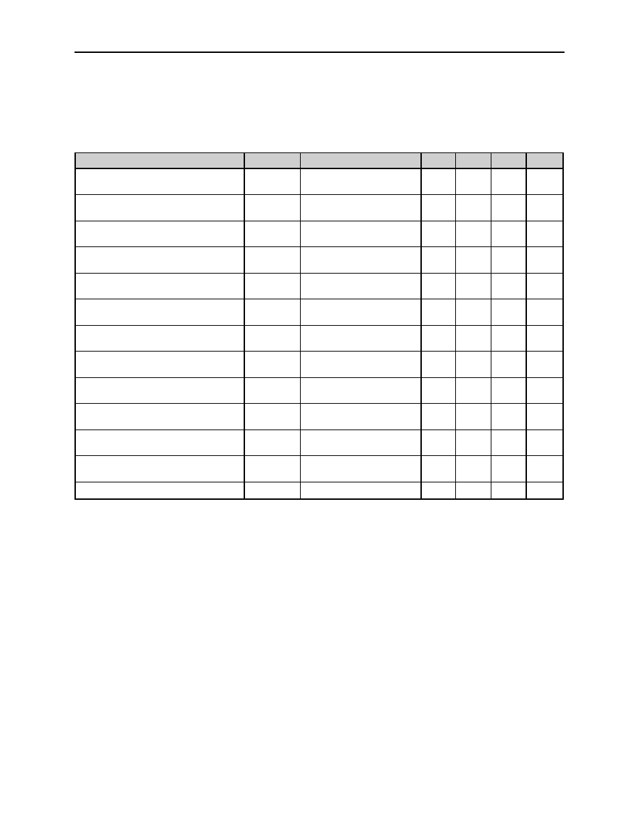
DC Electrical Characteristics
5 Electrical Characteristics
DC Electrical Characteristics
(
V
CC
= +3.0 to +3.6V, T
A
= -40 to +85∞C ,
R
L
= 100
, f
150Mhz
Typical values are at V
CC
= +3.3V, T
A
= +25∞C, Unless Otherwise Noted.)
1, 2
Notes:
1. Maximum and minimum limits over temperature are guaranteed by design and characterization. Devices are
100% tested at T
A
= +25∞C.
2. Currents into the device are positive, and current out of the device is negative. All voltages are referenced to
ground except V
OD
.
3. Guaranteed by correlation data.
Table 2. DC Electrical Characteristics
Parameter
Symbol
Conditions
Min
Typ
Max
Unit
LVDS Output (OUtx+, OUTx-)
Differential Output Voltage
V
OD
Figure 20 on page 12
250
370
450
mV
Change in Magnitude of V
OD
Between Complementary Output
States
V
OD
Figure 20 on page 12
1
35
mV
Offset Voltage
V
OS
Figure 20 on page 12
1.125
1.25
1.375
V
Change in Magnitude of V
OS
Between Complementary Output
States
V
OS
Figure 20 on page 12
4
25
mV
Output High Voltage
V
OH
1.6
V
Output Low Voltage
V
OL
0.90
V
Differential Output Short-Circuit
Current
3
I
OSD
Enabled, V
OD
= 0
-9
mA
Output Short-Circuit Current
I
OS
OUTx+ = 0 at INx = V
CC
or OUTx- = 0
at INx = 0, enabled
-3.8 -9
mA
Output High-Impedance
Current
I
OZ
EN = low and ENn = high, OUTx+ = 0
or V
CC
, OUTx- = 0 or V
CC
, R
L
=
-10 10
µA
Power-Off Output Current
I
OFF
V
CC
= 0 or open, OUTx+ = 0 or 3.6V,
OUTx- = 0 or 3.6V, R
L
=
-20 20
µA
Inputs (INx, EN, ENn)
High-Level Input Voltage
V
IH
2.0
V
CC
V
Low-Level Input Voltage
V
IL
GND 0.8
V
Input Current
I
IN
INx, EN, ENn = 0 or V
CC
-20 20
µA
Supply Current
No-Load Supply Current
I
CC
R
L
= ,
INx = V
CC
or 0 for all
channels
4 6
mA
Loaded Supply Current
I
CCL
R
L
= 100
, INx = V
CC
or 0 for all
channels
18 25
mA
Disabled Supply Current
I
CCZ
Disabled, INx = V
CC
or 0 for all
channels, EN = 0, ENn = V
CC
3.5
5.5
mA
www.austriamicrosystems.com
Revision 1.00
4 - 15
AS1152
austria
micro
systems
Data Sheet
Switching Characteristics
Switching Characteristics
(V
CC
= +3.0 to +3.6V, R
L
= 100
±1%, f
150MHz, T
A
= -40 to +85∞C
Typical values are at V
CC
= +3.3V, T
A
= +25∫C, Unless Otherwise Noted.)
1, 2, 3
Notes:
1. Parameters are guaranteed by design and characterization.
2. C
L
includes probe and jig capacitance.
3. Signal generator conditions for dynamic tests: V
OL
= 0, V
OH
= 3V, f = 100MHz, 50% duty cycle, RO = 50
,
t
R
1ns, t
F
1ns (0 to 100%).
4. t
SKD1
is the magnitude difference of differential propagation delay. t
SKD1
= |t
PHLD
- t
PLHD
|.
5. t
SKD2
is the magnitude difference of t
PHLD
or t
PLHD
of one channel to the t
PHLD
or t
PLHD
of another channel on
the same device.
6. t
SKD3
is the magnitude difference of any differential propagation delays between devices at the same V
CC
and
within 5∞C of each other.
7. t
SKD4
is the magnitude difference of any differential propagation delays between devices operating over the
rated supply and temperature ranges.
8. f
MAX
signal generator conditions: V
OL
= 0, V
OH
= 3V, 50% duty cycle, RO = 50
,
t
R
1ns, t
F
1ns (0 to 100%).
9. Conforms to ANSI TIA/EIA 644 LVDS Standards
150MHz. Maximum operating frequency of 250MHz is pos-
sible using an AS1150 receiver.
Table 3. Switching Characteristics
Parameter
Symbol
Conditions
Min
Typ
Max
Unit
Differential Propagation Delay,
High-to-Low
t
PHLD
Figure 18 on page 11 and
Figure 19 on page 11
1.1 1.7
ns
Differential Propagation Delay,
Low-to-High
t
PLHD
Figure 18 on page 11 and
Figure 19 on page 11
1.1
1.7
ns
Differential Pulse Skew
4
t
SKD1
Figure 18 on page 11 and
Figure 19 on page 11
0.04 0.35
ns
Differential Channel-to-Channel Skew
5
t
SKD2
Figure 18 on page 11 and
Figure 19 on page 11
0.07 0.60 ns
Differential Part-to-Part Skew
6
t
SKD3
Figure 18 on page 11 and
Figure 19 on page 11
0.13 0.8 ns
Differential Part-to-Part Skew
7
t
SKD4
Figure 18 on page 11 and
Figure 19 on page 11
0.43 1.0
ns
Rise Time
t
TLH
Figure 18 on page 11 and
Figure 19 on page 11
0.2 0.39 2.6 ns
Fall Time
t
THL
Figure 18 on page 11 and
Figure 19 on page 11
0.2 0.39 2.6
ns
Disable Time, High-to-Z
t
PHZ
Figure 21 on page 12 and
Figure 22 on page 12
3 4 ns
Disable Time, Low-to-Z
t
PLZ
Figure 21 on page 12 and
Figure 22 on page 12
3 4
ns
Enable Time, Z-to-High
t
PZH
Figure 21 on page 12 and
Figure 22 on page 12
2
3
ns
Enable Time, Z-to-Low
t
PZL
Figure 21 on page 12 and
Figure 22 on page 12
2
3
ns
Maximum Operating Frequency
8, 9
f
MAX
250
MHz
www.austriamicrosystems.com
Revision 1.00
5 - 15
AS1152
austria
micro
systems
Data Sheet
Switching Characteristics
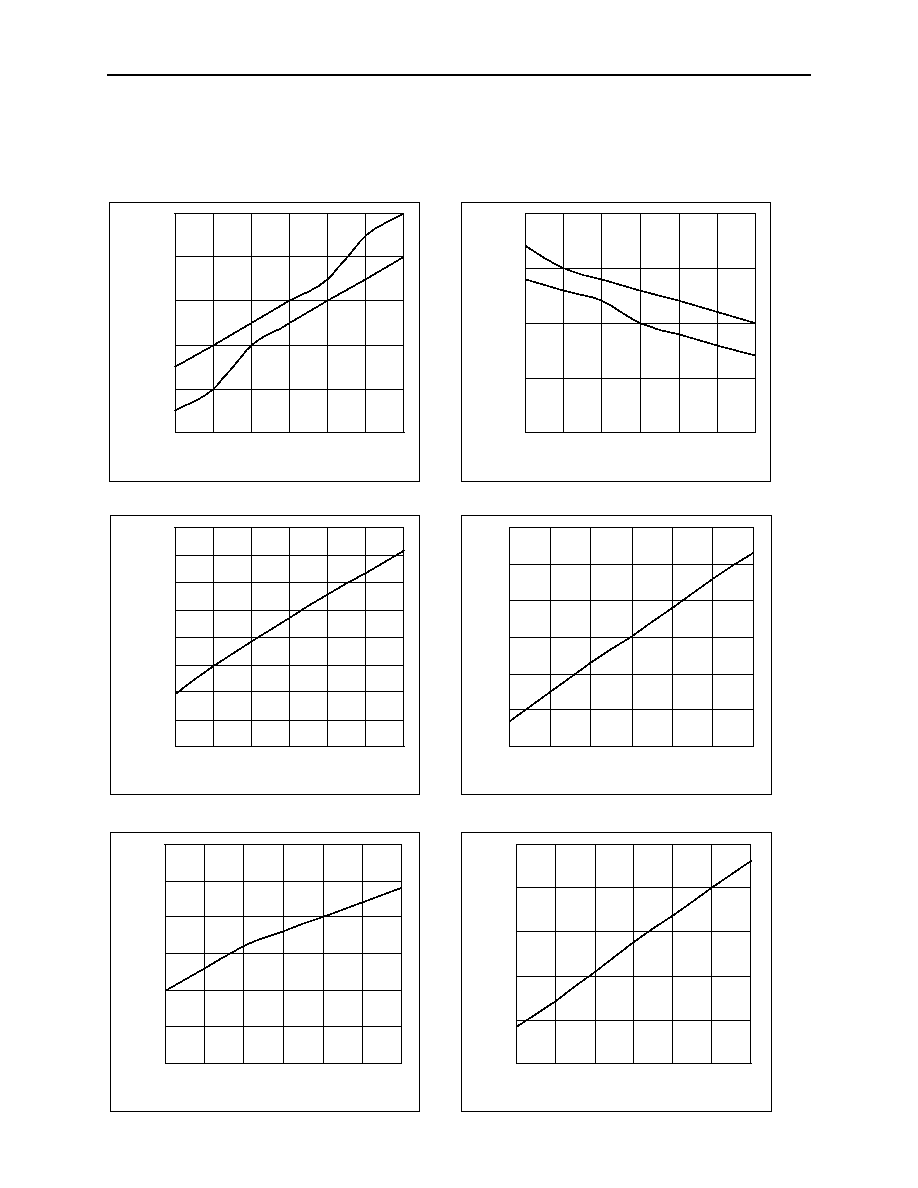
6 Typical Operating Characteristics
V
CC
= +3.3V, V
CM
= +1.2V, |V
ID
| = 0.2V, C
LOAD
= 15pF, Tamb = +25∫C, unless otherwise noted
Figure 2. Output High Voltage vs. V
CC
Figure 3. Output Low Voltage vs. V
CC
Figure 4. Output Short-Circuit Current vs. V
CC
;
Figure 5. Output High-Impedance State Current vs.
V
IN
= V
CC
or GND
V
CC
; V
IN
= V
CC
or GND
Figure 6. Differential Output Voltage vs. V
CC
Figure 7. Differential Output Voltage vs. Load
Resistor
1.4
1.402
1.404
1.406
1.408
1.41
3
3.1
3.2
3.3
3.4
3.5
3.6
Power-Supply Voltage (V)
O
u
t
put
High
V
o
lt
a
ge (
V
)
.
V
OUT-
V
OUT+
1.06
1.065
1.07
1.075
1.08
3
3.1
3.2
3.3
3.4
3.5
3.6
Power-Supply Voltage (V)
O
u
t
p
ut
L
o
w V
o
lt
age (
V
)
.
V
OUT-
V
OUT+
3.500
3.525
3.550
3.575
3.600
3.625
3.650
3.675
3.700
3
3.1
3.2
3.3
3.4
3.5
3.6
Power-Supply Voltage (V)
O
u
t
put
S
hor
t
-
Cir
c
uit
Cur
r
ent
(
m
A
)
.
24
25
26
27
28
29
30
3
3.1
3.2
3.3
3.4
3.5
3.6
Power-Supply Voltage (V)
O
u
t
p
ut
H
i
gh-
Z
S
t
at
e
Cur
r
e
n
t
(
µ
A
)
.
320
325
330
335
340
345
350
3
3.1
3.2
3.3
3.4
3.5
3.6
Power-Supply Voltage (V)
Di
f
f
e
r
e
n
t
ial
O
u
t
put
V
o
lt
ag
e (
V
)
.
250
300
350
400
450
500
90
100
110
120
130
140
150
Load Resistor (Ohm)
D
i
f
f
er
ent
i
a
l O
u
t
put
V
o
lt
age (
m
V
)
.

www.austriamicrosystems.com
Revision 1.00
6 - 15
AS1152
austria
micro
systems
Data Sheet
Switching Characteristics
Figure 8. Offset Voltage vs. V
CC
Figure 9. Power Supply Current vs. Frequency;
V
IN
= 0 to 3V
Figure 10. I
CC
vs. V
CC
; Freq = 1MHz
Figure 11. I
CC
vs. Temperature; Freq = 1MHz
Figure 12. Differential Propagation Delay vs. V
CC
;
Figure 13. Differential Propagation Delay vs.
Freq = 1MHz
Temperature; Freq = 1MHz
1.24
1.241
1.242
1.243
1.244
3
3.1
3.2
3.3
3.4
3.5
3.6
Power-Supply Voltage (V)
O
f
f
s
e
t
V
o
lt
age
(
V
)
.
10
20
30
40
50
60
0.1
1
10
100
1000
Frequency (MHz)
Po
w
e
r-S
u
p
p
l
y
C
u
rre
n
t
(mA)
.
All Channels
One Channels
18
18.25
18.5
18.75
19
19.25
19.5
3
3.1
3.2
3.3
3.4
3.5
3.6
Power-Supply Voltage (V)
Po
w
e
r-S
u
p
p
l
y
C
u
rre
n
t
(mA)
.
17
18
19
20
21
22
-50
-30
-10
10
30
50
70
90
Temperature(∞C)
Po
w
e
r-S
u
p
p
l
y
C
u
rre
n
t
(mA)
.
1.1
1.2
1.3
1.4
1.5
1.6
3
3.1
3.2
3.3
3.4
3.5
3.6
Power-Supply Voltage (V)
Dif
f
.
P
r
opa
gat
i
on De
lay
(
n
s
)
.
1.1
1.2
1.3
1.4
1.5
1.6
-50
-30
-10
10
30
50
70
90
Temperature (∞C)
Dif
f
.
P
r
opa
gat
i
on De
lay
(
n
s
)
.
t
PHLD
t
PLHD
t
PHLD
t
PLHD

www.austriamicrosystems.com
Revision 1.00
7 - 15
AS1152
austria
micro
systems
Data Sheet
Switching Characteristics
Figure 14. Differential Skew vs. V
CC
;
Figure 15. Differential Skew vs. Temperature;
Freq = 1MHz
Freq = 1MHz
0
30
60
90
120
150
3
3.1
3.2
3.3
3.4
3.5
3.6
Power Supply Voltage (V)
D
i
ff
.
P
u
l
s
e
S
k
e
w
(
p
s
)
.
0
30
60
90
120
150
-50
-30
-10
10
30
50
70
90
Temperature (∞C)
D
i
ff
.
P
u
l
s
e
S
k
e
w
(
p
s
)
.

www.austriamicrosystems.com
Revision 1.00
8 - 15
AS1152
austria
micro
systems
Data Sheet
Pin Assignments
7 Pinout and Packaging
Pin Assignments
Figure 16. AS1152 Pin Assignments (Top View)
Pin Descriptions
Table 4. AS1152 Pin Descriptions
Pin Number
Pin Name
Description
1
EN
Driver Enable Input. Internally pulled down to GND.
When EN = high and ENn = low or open, the driver outputs are active. For other
combinations of EN and ENn, the outputs are disabled and in high impedance.
2
IN1
LVTTL/LVCMOS Driver Input
3
IN2
LVTTL/LVCMOS Driver Input
4
V
CC
Power Supply Input. Bypass V
CC
to GND with 0.1µF and 0.001µF ceramic
capacitors.
5
GND
Ground
6
IN3
LVTTL/LVCMOS Driver Input
7
IN4
LVTTL/LVCMOS Driver Input
8
ENn
Driver Enable Input. Internally pulled down to GND.
When EN = high and ENn = low or open, the driver outputs are active. For other
combinations of EN and ENn, the outputs are disabled and in high impedance.
9
OUT4-
Inverting LVDS Driver Output
10
OUT4+
Noninverting LVDS Driver Output
11
OUT3+
Noninverting LVDS Driver Output
12
OUT3-
Inverting LVDS Driver Output
13
OUT2-
Inverting LVDS Driver Output
14
OUT2+
Noninverting LVDS Driver Output
15
OUT1+
Noninverting LVDS Driver Output
16
OUT1-
Inverting LVDS Driver Output
OUT1-
OUT1+
OUT2+
OUT2-
OUT3-
OUT3+
OUT4+
OUT4-
EN
IN1
IN2
V
CC
GND
IN3
IN4
ENn
AS1152
TSSOP
1
2
3
4
5
6
7
8
16
15
14
13
12
11
10
9

www.austriamicrosystems.com
Revision 1.00
9 - 15
AS1152
austria
micro
systems
Data Sheet
LVDS Interface
8 Detailed Description
LVDS Interface
The LVDS interface standard is a signaling method intended for point-to-point communication over a controlled-imped-
ance medium as defined by the ANSI/TIA/EIA-644 and IEEE 1596.3 standards. The LVDS standard uses a lower volt-
age swing than other common communication standards, achieving higher data rates with reduced power
consumption while reducing EMI emissions and system susceptibility to noise.
The AS1152 is an 500Mbps quad differential LVDS driver that is designed for high-speed, point-to-point, low-power
applications. This device accepts LVTTL/LVCMOS input levels and translates them to LVDS output signals.
The AS1152 generates a 2.5mA to 4.5mA output current using a current-steering configuration. This current steering
approach induces less ground bounce and no shoot-through current, enhancing noise margin and system speed per-
formance. The driver outputs are short-circuit current limited, and enter a high-impedance state when the device is not
powered or is disabled.
The current-steering architecture of the AS1152 requires a resistive load to terminate the signal and complete the
transmission loop. Because the device switches current and not voltage, the actual output voltage swing is determined
by the value of the termination resistor at the input of an LVDS receiver (AS1150, AS1151). Logic states are deter-
mined by the direction of current flow through the termination resistor.
With a typical 3.7mA output current, the AS1152 produces an output voltage of 370mV when driving a 100
load.
Note: The AS1152 is conform to the ANSI TIA/EIA 644 LVDS Standards when operating
150MHz. Paired with the
AS1150 the datarate can be increased to 500Mbps. While operating faster then 150MHz, the rise and fall time,
as well as the setup and hold time are not conform to the ANSI TIA/EIA 644 LVDS Standards.
Termination
Because the AS1152 is a current-steering device, no output voltage will be generated without a termination resistor.
The termination resistors should match the differential impedance of the transmission line. Output voltage levels
depend upon the value of the termination resistor.
The AS1152 is optimized for point-to-point interface with 100
termination resistors at the receiver inputs. Termination
resistance values may range between 90 and132
, depending on the characteristic impedance of the transmission
medium.

www.austriamicrosystems.com
Revision 1.00
10 - 15
AS1152
austria
micro
systems
Data Sheet
Power-Supply Bypassing
9 Applications
Figure 17. Typical Application Circuit
Power-Supply Bypassing
To bypass V
CC
, use high-frequency surface-mount ceramic 0.1µF and 0.001µF capacitors in parallel as close to the
device as possible, with the smaller valued capacitor closest to pin V
CC
.
Differential Traces
Input trace characteristics can adversely affect the performance of the AS1152.
!
Use controlled-impedance PC board traces to match the cable characteristic impedance. The termination resistor is
also matched to this characteristic impedance.
!
Eliminate reflections and ensure that noise couples as common mode by running the differential traces near each
other.
!
Reduce skew by using matched trace lengths. Tight skew control is required to minimize emissions and proper data
recovery of the devices.
!
Route each channel's differential signals very close to each other for optimal cancellation of their respective exter-
nal magnetic fields. Use a constant distance between the differential traces to avoid irregularities in differential
impedance.
!
Avoid 90∞ turns (use two 45∞ turns).
!
Minimize the number of vias to further prevent impedance irregularities.
Table 5. Function Table
Enable Pins
Input
Output
EN
ENn
INx+
INx-
OUTx
H
L or Open
L
L
H
H
L or Open
H
H
L
Other Combinations of Enable Pin Settings
Don't Care
Z
Z
LVDS
Signals
107
107
107
107
LVTTL/LVCMOS
Data Inputs
LVTTL/LVCMOS
Data Outputs
100
Shielded Twisted Cable or Microstrip PC Board Traces
Tx
Tx
Tx
Tx
Rx
Rx
Rx
Rx
AS1151
Quad LVDS Receiver
AS1152

www.austriamicrosystems.com
Revision 1.00
11 - 15
AS1152
austria
micro
systems
Data Sheet
Cables and Connectors
Supported transmission media include printed circuit board traces, backplanes, and cables.
!
Use cables and connectors with matched differential impedance (typically 100
) to minimize impedance mis-
matches.
!
Balanced cables such as twisted pair offer superior signal quality and tend to generate less EMI due to magnetic
field canceling effects. Balanced cables pick up noise as common mode, which is rejected by the LVDS receiver.
!
Avoid the use of unbalanced cables such as ribbon cable or simple coaxial cable.
Board Layout
The device should be placed as close to the interface connector as possible to minimize LVDS trace length.
!
Keep the LVDS and any other digital signals separated from each other to reduce crosstalk.
!
Use a four-layer PC board that provides separate power, ground, LVDS signals, and input signals.
!
Isolate the input LVDS signals from each other and the output LVCMOS/LVTTL signals from each other to prevent
coupling.
!
Separate the input LVDS signals from the output signals planes with the power and ground planes for best results.
Figure 18. Driver Propagation Delay and Transition Time Waveforms
Figure 19. Driver Propagation Delay and Transition Time Test Circuit
t
THL
t
TLH
t
PLHD
t
PHLD
0 Differential
1.5V
20%
80%
0
20%
OUTx-
OUTx+
INx
V
OH
V
OL
0
1.5V
V
DIFF
= (V
OUT
x
+
) - (V
OUT
x
-
)
80%
0
OUTx-
Generator
50
R
L
OUTx+
INx

www.austriamicrosystems.com
Revision 1.00
12 - 15
AS1152
austria
micro
systems
Data Sheet
Figure 20. Driver V
OD
and V
OS
Test Circuit
Figure 21. Driver High Impedance Delay Waveforms
Figure 22. Driver High-Impedance Delay Test Circuit
V
OS
V
OD
OUTx+
OUTx-
R
L
/2
R
L
/2
V
CC
GND
INx
1.5V
EN when ENn = 0 or Open
ENn when EN = V
CC
1.5V
1.5V
1.5V
50%
50%
3V
0
V
OL
V
OH
1.2V
t
PZL
t
PLZ
OUTx+ When INx = V
CC
OUTx- When INx = 0
0
3V
t
PZH
t
PHZ
50%
50%
1.2V
OUTx+ When INx = 0
OUTx- When INx = V
CC
V
CC
Generator
50
R
L
/2
ENn
EN
GND
INx
OUTx+
OUTx-
R
L
/2
+1.2V
1/4 AS1152
www.austriamicrosystems.com
Revision 1.00
13 - 15
AS1152
austria
micro
systems
Data Sheet
Board Layout
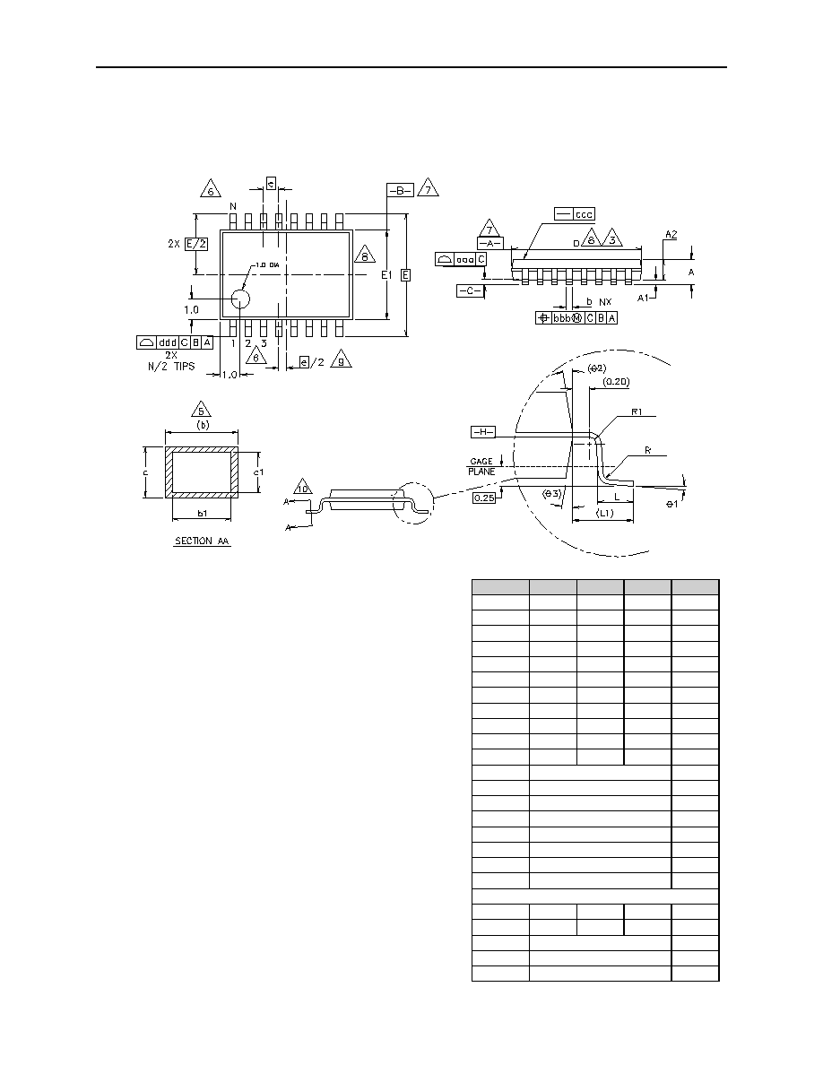
10 Package Drawings and Markings
Figure 23. 16-pin TSSOP Package
Symbol
Min
Typ
Max
Notes
A
-
-
1.10
1,2
A1
0.05
-
0.15
1,2
A2
0.85
0.90
0.95
1,2
L
0.50
0.60
0.75
1,2
R
0.09
-
-
1,2
R1
0.09
-
-
1,2
b
0.19
-
0.30
1,2,5
b1
0.19
0.22
0.25
1,2
c
0.09
-
0.20
1,2
c1
0.09
-
0.16
1,2
1
0∫
-
8∫
1,2
L1
1.0REF
1,2
aaa
0.10
1,2
bbb
0.10
1,2
ccc
0.05
1,2
ddd
0.20
1,2
e
0.65BSC
1,2
2
12∫REF
1,2
3
12∫REF
1,2
Variations
D
4.90
5.00
5.10
1,2,3,8
E1
4.30
4.40
4.50
1,2,4,8
E
6.4BSC
1,2
e
0.65BSC
1,2
N
16
1,2,6
Notes:
1. All dimensions are in millimeters; angles in degrees.
2. Dimensioning and tolerancing per ASME Y14.5M ≠ 1994.
3. Dimension D does not include mold flash, protrusions, or gate
burrs. Mold flash, protrusions, and gate burrs shall not exceed
0.15mm per side.
4. Dimension E1 does not include interlead flash or protrusion.
Interlead flash or protrusions shall not exceed 0.25mm per
side.
5. Dimension b does not include dambar protrusion. Allowable
dambar protrusion shall be 0.08mm total in excess of the b
dimension at maximum material condition. Dambar cannot be
located on the lower radius of the foot.
6. Terminal numbers are for reference only.
7. Datums A and B to be determined at datum plane H.
8. Dimensions D and E1 are to be determined at datum plane H.
9. This dimension applies only to variations with an even number
of leads per side.
10. Cross section A-A to be determined at 0.10 to 0.25mm from
the leadtip.

www.austriamicrosystems.com
Revision 1.00
14 - 15
AS1152
austria
micro
systems
Data Sheet
Board Layout
11 Ordering Information
Part Number
Description
Package Type
Delivery Form
AS1152
Quad low-voltage differential signaling driver
16-pin TSSOP
Tube
AS1152-T
Quad low-voltage differential signaling driver
16-pin TSSOP
Tape and Reel

www.austriamicrosystems.com
Revision 1.00
15 - 15
AS1152
austria
micro
systems
Data Sheet
Board Layout
Copyrights
Copyright © 1997-2005, austriamicrosystems AG, Schloss Premstaetten, 8141 Unterpremstaetten, Austria-Europe.
Trademarks Registered Æ. All rights reserved. The material herein may not be reproduced, adapted, merged, trans-
lated, stored, or used without the prior written consent of the copyright owner.
All products and companies mentioned are trademarks or registered trademarks of their respective companies.
Disclaimer
Devices sold by austriamicrosystems AG are covered by the warranty and patent indemnification provisions appearing
in its Term of Sale. austriamicrosystems AG makes no warranty, express, statutory, implied, or by description regarding
the information set forth herein or regarding the freedom of the described devices from patent infringement. austriami-
crosystems AG reserves the right to change specifications and prices at any time and without notice. Therefore, prior
to designing this product into a system, it is necessary to check with austriamicrosystems AG for current information.
This product is intended for use in normal commercial applications. Applications requiring extended temperature
range, unusual environmental requirements, or high reliability applications, such as military, medical life-support or life-
sustaining equipment are specifically not recommended without additional processing by austriamicrosystems AG for
each application.
The information furnished here by austriamicrosystems AG is believed to be correct and accurate. However,
austriamicrosystems AG shall not be liable to recipient or any third party for any damages, including but not limited to
personal injury, property damage, loss of profits, loss of use, interruption of business or indirect, special, incidental or
consequential damages, of any kind, in connection with or arising out of the furnishing, performance or use of the tech-
nical data herein. No obligation or liability to recipient or any third party shall arise or flow out of
austriamicrosystems AG rendering of technical or other services.
Contact Information
Headquarters
austriamicrosystems AG
A-8141 Schloss Premstaetten, Austria
Tel: +43 (0) 3136 500 0
Fax: +43 (0) 3136 525 01
For Sales Offices, Distributors and Representatives, please visit:
http://www.austriamicrosystems.com
austria
micro
systems
≠ a leap ahead in mixed signal