 | ÐлекÑÑоннÑй компоненÑ: AS5021-E | СкаÑаÑÑ:  PDF PDF  ZIP ZIP |
Microsoft Word - AS5021-E_datasheet.doc
Revision December 2002
Page 1 of 8
Key Features
-
2 channel quadrature TTL squarewave outputs (A/B) with
16 pulses per revolution
-
Rotary direction information available
-
Optional 3
rd
channel index (one pulse per revolution)
which is user programmable. This allows cost effective
manufacturing of the encoder system.
-
Rotation speed of magnetic source up to 30,000 rpm
-
Extended temperature range: - 40° C to +125° C
(-40° F to +257° F)
-
System on Chip: Hall effect sensors and signal
processing combined on a single chip
-
Simple permanent magnetic source required
Benefits
-
Non-contact switching providing high reliability and
long mechanical life time. Ideal for electrically isolated
applications.
-
Extremely compact SOIC-8 package
-
Ease of implementation with reduced number of external
components
-
No calibration needed
-
Extremely tolerant to magnetic and harsh environment
-
Tolerant to magnetic source misalignment
Applications
-
Motor control
-
Incremental encoders
-
Precision angular position sensing
-
Angular Speed Sensing
-
Motion control
General Description
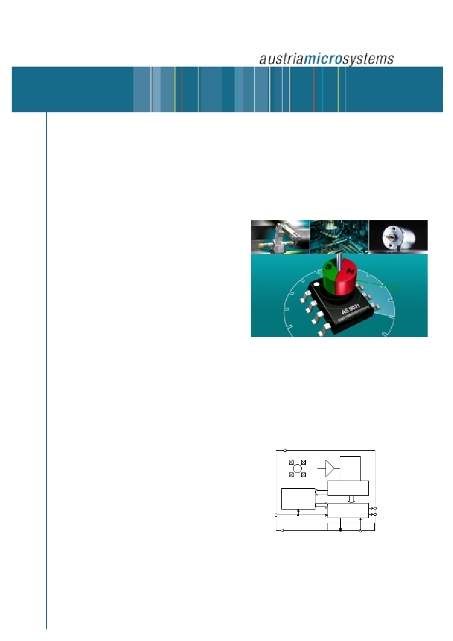
The AS5021 device provides a 2 x 16 pulse quad A/B signal
within one rotation, encoding 64 state changes. These
incremental steps are encoded by a simple magnet source
that is placed above the device surface. A total of 64
incremental angular positions are available within the full
360° range (typical step size: 5.625° ).
Figure 1
Placement of AS5021 device and magnet source
The optional 3
rd
channel index (one pulse per revolution) is
user programmable and allows one time programming of a
user specific index-position between the device and the
magnet source.
The device includes a Hall sensor array as well as the signal
conditioning and the post processing circuits. Figure 2 shows
the working principal of the AS5021 device.
6bit
ADC
Measurement
Register
Adder & Output-
Register
OTP-ROM
Index-Position
Programming
-
+
Sensor-Array
VDD
PROG
GND
A
CSn
Index
B
Figure 2
Block diagram
DATA SHEET
AS5021-E
INCREMENTAL ROTARY ENCODER
(Extended Temperature Range)
AS5021 - INCREMENTAL ROTARY ENCODER
Revision December 2002
Page 2 of 8
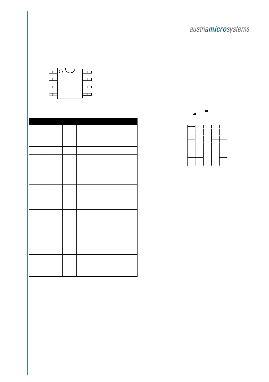
Pin Configuration
A
B
N.C.
N.C.
CSn/ Index
PROG
VSS
VDD
Pin Description
Pin #
Symbol
Type
Description
1
B
DO
This pin represents signal B of quad
A/B outputs. Signal B changes the
state every 11.25° and is shifted
5.625° relative to signal A.
2
V
DD
AI
Positive Supply Voltage.
3
V
S S
AI
Negative Supply Voltage (GND).
4
PROG
DI
PROGramming Input
This pin is used to program the index
position into a non-volatile memory
(One Time Programmable).
5
N.C.
AI
Not Connected during operation. This
pin is for manufacturers use only
6
N.C.
AI
Not Connected during operation. This
pin is for manufacturer's use only.
7
CSn/
Index
DIO
Chip Select (active low)
CSn=0 activates the device and
enables measurement.
Index
After programming an user specific
index position this pin provides one
index pulse per revolution. A version
with pre-programmed index can be
delivered.
8
A
DO
This pin represents signal A of quad
A/B outputs. Signal A changes the
state every 11.25° and is shifted
5.625° relative to signal B.
DI:
Digital Input
AI:
Analogue Input
DO:
Digital Output
DIO:
Digital Input Output
Note:
Pins 4, 5 and 6 may be either left open or
connected together
Functional Description
A Hall sensor array is used to convert the magnetic field
distributed above the chip surface into a quadrature output
signal. Any angular change of 5.625° results in a change in
state of either A or B output.
Figure 3 shows the changing of the quad A/B signal in
clockwise (CW) and counter-clockwise (CCW) direction.
A
0
C W
B
1
1
0
0
0
1
1
C C W
5 . 6 2 5
Figure 3
Quadrature A/B signal
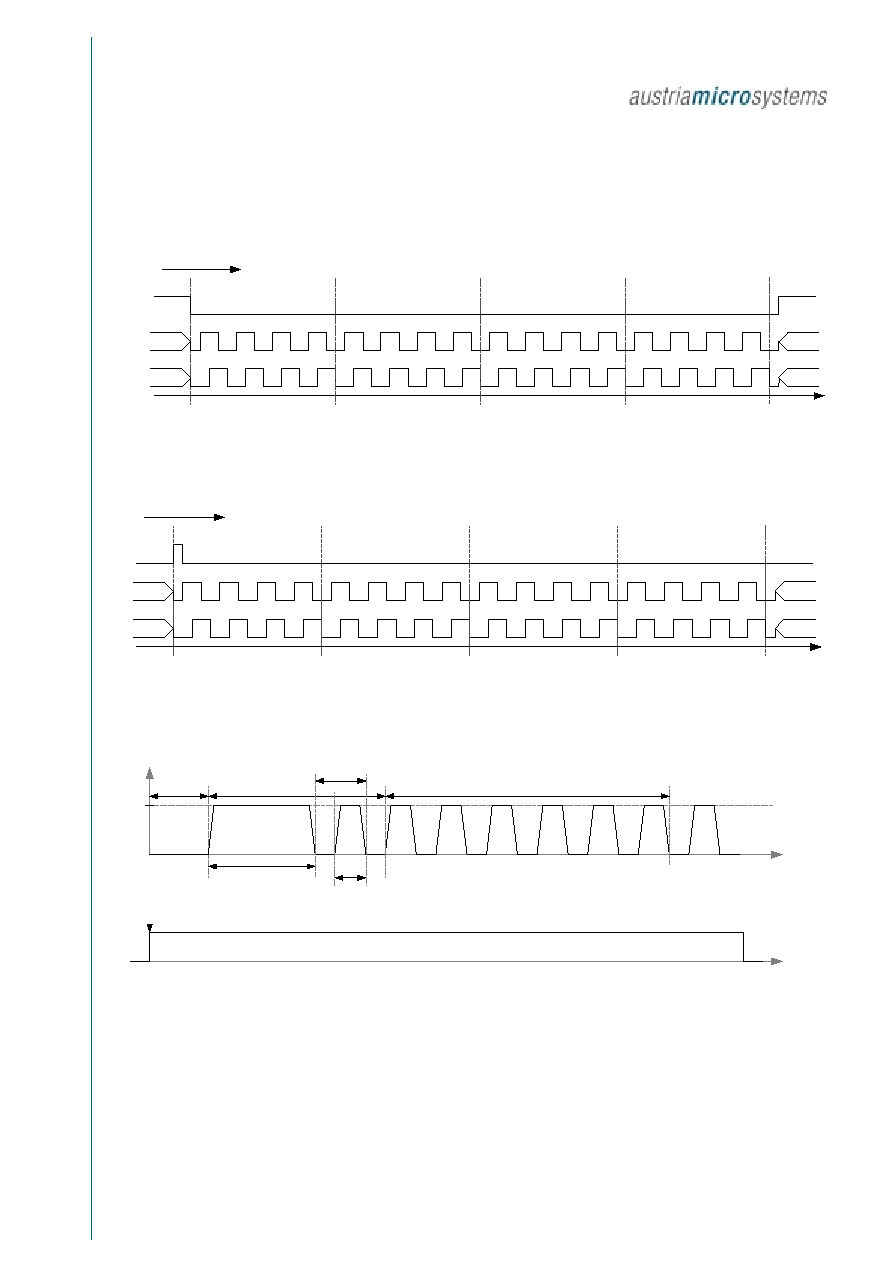
Figure 4 shows the output signals A and B for one full 360°
rotation. 16 pulses per revolution, each interpolating 4
position changes, lead to a resolution of 64 increments over
360° with a maximum output frequency of 8,000 Hz.
Chip Select must be active low (CSn=0) to enable
measurement and to activate the output pin A and B
(pin 8 and 1).
Pin A and pin B change the state every 11.25° . The 90
degree phase shift between channel A and B indicates the
direction of the magnet's movement. Channel A leads
channel B by 5.625 degree for a clockwise rotation of the
rotor viewed from the encoder cover. Channel B leads
channel A for a counter clockwise rotation of the rotor.
With Chip Select at logic high, the device returns to the
power down state. A and B becomes high ohmic (e.g. for use
in bus systems).
The AS5021 is extremely tolerant tof magnetic misalignment
and to environmental influences due to the design adopted
for the ratiometric measurement and Hall sensor conditioning
circuitry.
Due to the very high level of system integration, the AS5021
allows for easy implementation of an angular measurement
system. Only two external components, a magnetic field
source and a de-coupling capacitor, are required.
AS5021 - INCREMENTAL ROTARY ENCODER
Revision December 2002
Page 3 of 8
Timing Diagrams
A
CSn
360°
0°
clockwise movement of magnet
high Z
high Z
high Z
high Z
B
270°
180°
90°
Figure 4
Output signals A and B for one full 360° rotation in standard mode
A
Index
360°
0°
clockwise movement of magnet
high Z
high Z
high Z
high Z
B
270°
180°
90°
programmable default 0°
Figure 5
Output signals A, B and index for one full 360° rotation in continuous read out mode
Dummy
2
3
4
5
6
7
8
9
1
Enable
Programming
8
0
PROG
Initialization
t
wait
Index Position Programming
t
Enable Index
Bit0
Bit5
Bit4
Bit3
Bit2
Bit1
Measurement
Enable
CSn
Calibration Position
Latched
t
ProgEN
t
Zap
t
Prog
Figure 6
Programming sequence
AS5021 - INCREMENTAL ROTARY ENCODER
Revision December 2002
Page 4 of 8
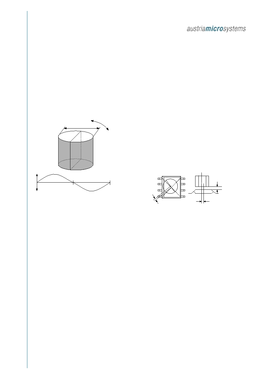
As illustrated in figure 7, a simple two-pole permanent
magnet may be used as the magnetic field source.
The magnet may be a diametrically magnetized, cylindrical
standard magnet. Magnetic materials such as rare earth
AlNiCo / SmCo5 or NdFeB are recommended. Typically, the
magnet size should be 3 to 6mm in diameter and 2 to 3mm in
height. The typical distance between the magnet and the
device is 0.5 to 1.5 mm.
A magnetic field strength of typically
±40mT is required at
the package surface and a diameter of 1.6 mm.
3 - 6mm
S
N
40
-40
S
N
180°
360°
/ °
B/mT
Figure 7
Typical magnet and magnetic field at the diameter of 1.5mm
Programming of Index Pulse
The possibility to program the optional 3rd channel index
pulse at a user specific position gives many advantages (e.g.
it simplifies the assembly at the production line, as the
orientation of the magnet does not need to be considered).
Figure 6 shows the timing diagram for programming the user
specific index pulse (one pulse per revolution). The typical
values are shown in the table on page 5.
Before programming the user specific index position the
magnet must be adjusted in measurement mode (CSn=0).
The rising edge of CSn measures the actual position between
the device and the magnetic source and stores it internally
for the permanent programming CSn must be high during the
whole programming sequence.
The first 8V pulse after the minimum waiting time t
w ait
sets the
device into programming mode. It is important that this first
pulse has a minimum duration of t
p r og E N
= 200 µ s. The
following 7 pulses with 8V/5
µs select the latched position
information and permanently write the reference value into
the OTP ROM. The 9th pulse enables the index.
The index pulse at pin 7 will be available after switching the
power off and on again.
Physical Placement of the Magnet
The magnet may be placed above or below the device. The
distance must be within the specified range and the rotation
axis should be aligned to the device center.
The recommended axis point is given by the crossing of the
diagonals with respect to the leadframe.
Accurate placement is important to achieve the specified
accuracy with respect to the temperature and the voltage
ranges. Figure 8 shows the maximum allowed misalignment
of the magnet with respect to the device, the typical values
are shown in the table on page 6.
Referenced to pins
R
Disp
R
Disp
Z
Dist
Figure 8
Maximum allowed misalignment of magnet with respect to
the device
If placement tolerances are larger than specified, the device
continues to operate at a reduced linearity performance.
AS5021 - INCREMENTAL ROTARY ENCODER
Revision December 2002
Page 5 of 8
Electrical Characteristics
Absolute Maximum Ratings
Symbol
Parameter
Remarks
Min
Typ
Max
Unit
V
DD
Max. Supply Voltage
-0.3
7
V
I
L UI
Max. Input Current
Latch-up immunity /
Norm JEDEC 17
25
mA
V
I N
Max. Digital Input Voltage
-0.3
V
DD
+ 0.3
V
ESD
Electrostatic Discharge
Norm MIL883E method 3015
-1000
+1000
V
T
S to re
Storage Temperature Range
-50
+125
° C
P
t ot
Total Power Dissipation
150
mW
H
Humidity non-condensing
5
85
%
Soldering Conditions
Norm: IEC 6170-1
0.7 V
DD
V
DD
V
Stresses beyond those listed under "Absolute Maximum Ratings" may cause permanent damage to the device. These are stress
ratings only. Functional operation of the device at these or any other conditions beyond those indicated under "Operating
Conditions" is not implied. Exposure to absolute maximum rating conditions for extended periods may affect device reliability.
Operating Conditions
Symbol
Parameter
Conditions
Min
Typ*
Max
Unit
V
DD
Supply Voltage
Measurement mode, V
S S
=0V
4.75
5.0
5.25
V
T
A MB
Ambient Operating Temp. Range
-40
+125
° C
V
I L
Input Low Voltage
V
S S
0.3 V
DD
V
V
I H
Input High Voltage**
0.7 V
DD
V
DD
V
Note: External Buffer Capacitance is needed: e.g. 4.7µ F between the supply pins
* typical figures at 25° C are for design aid only; not guaranteed and not subjected to production testing.
** At pin PROG a higher voltage (up to 8.5V) is defined for the zero position programming routine.
DC Characteristics
Symbol
Parameter
Conditions
Min
Typ
Max
Unit
I
DD
Operating Supply Current
CSn=0, Continuous Mode
15
24
mA
I
O
Digital Output Current Capability
4
mA
Programming Input
(see Figure 6)
Symbol
Parameter
Conditions
Min
Typ*
Max
Unit
V
P ROG
Programming Voltage
Measurement mode, V
S S
=0V
8
8.5
V
t
Zap
Zap Pulse Duration
4.5
5
5.5
µ s
t
P ro g
Programming Period
9
10
11
µ s
t
Wa it
Minimum Waiting Time after
Rising Edge of CSn
0.5
µ s
t
P ro gE N
Delay after CSn=1
200
µ s
T
L H
Pulse Slew Rate
2
V/µ s
I
P ROG
Programming Current
100
mA