
Copyright ANPEC Electronics Corp.
Rev. C.1 - Jun., 2003
APL431
www.anpec.com.tw
1
ANPEC reserves the right to make changes to improve reliability or manufacturability without notice, and advise
customers to obtain the latest version of relevant information to verify before placing orders.
Adjustable Precision Shunt Regulator
Features
General Description
Applications
The APL431 is a 3-terminal adjustable voltage refer-
ence with specified thermal stability over applicable
commercial temperature ranges. Output voltage may
be set to any value between V
ref
(2.5 V) and 20 V with
two external resistors (see Figure 2). When used
with an photocoupler, the APL431 is an ideal voltage
reference in isolated feedback circuits for 2.5V to 12V
switching-mode power supplies. This device has a
typical output impedance of 0.1
. Active output cir-
cuitry provides a very sharp turn-on characteristic,
making the APL431 excellent replacements for ze-
ner diodes in many applications, including on-board
regulation and adjustable power supplies.
∑∑
∑∑
∑
Precise Reference Voltage to 2.500V
∑∑
∑∑
∑
Guaranteed 0.5%, 1% or 2% Reference
Voltage Tolerance
∑∑
∑∑
∑
Sink Current Capability, 1mA to 100mA
∑∑
∑∑
∑
Quick Turn-on
∑∑
∑∑
∑
Adjustable Output Voltage, V
O
= V
ref
to 20V
∑∑
∑∑
∑
Low Operational Cathode Current, 250µA
Typical
∑∑
∑∑
∑
0.1
Typical Output Impedance
∑∑
∑∑
∑
SOT-23, SOT-23-5, SOT-89, SO-8, TO-92
and TO-92S Packages
∑∑
∑∑
∑
Linear Regulators
∑∑
∑∑
∑
Adjustable Power Supply
∑∑
∑∑
∑
Switching Power Supply
Cathode
Anode
REF
Symbol
Functional Diagram
V
ref
+
_
Cathode
REF
Anode
SOT-23 (Top View)
REF
ANODE
CATHODE
1
2
3
SOT-89 (Top View)
REF
ANODE CATHODE
1
2
3
REF
ANODE
CATHODE
3
2
1
TO-92 (Top View)
SO-8 (Top View)
REF
ANODE
CATHODE
ANODE
NC
ANODE
ANODE
NC
1
2
3
4
8
7
6
5
REF ANO DE
NC
NC
CATHO DE
1
2
3
4
5
SOT-23-5 (Top View)
REF
ANODE
CATHODE
3
2
1
TO-92S (Top View)

Copyright ANPEC Electronics Corp.
Rev. C.1 - Jun., 2003
APL431
www.anpec.com.tw
2
Symbol
Parameter
Rating
Unit
V
KA
Cathode voltage
20
V
I
K
Continuous cathode current range
100
mA
I
REF
Reference current range
3
mA
JA
Thermal Resistance from Junction to Ambient in Free Air
SOT-23
SOT-23-5
SOT-89
TO-92
SO-8
416
357
250
250
210
∞C/W
T
A
Ambient temperature range APL431XXC
APL431XXI
0 to 70
-40 to 85
∞C
T
j
Junction temperature range APL431XXC
APL431XXI
0 to 150
-40 to 150
∞C
T
STG
Storage Temperature Range
-65 to 150
∞C
Lead temperature range, T
s
(Soldering, 10sec)
Original Device
260
T
SOL
Lead Free Device
300
∞C
Ordering and Marking Information
A P L 4 3 1
E le c . G ra d e
H a n d lin g C o d e
T e m p . R a n g e
P a c k a g e C o d e
E le c . G ra d e
A : 0 .5 % R e fe re n c e V o lta g e T o le ra n c e
B : 1 % R e fe re n c e V o lta g e T o le ra n c e
C : 2 % R e fe re n c e V o lta g e T o le ra n c e
P a c k a g e C o d e
A : S O T -2 3 B : S O T -2 3 -5 D : S O T -8 9
E : T O -9 2 I : T O -9 2 S K : S O -8
Y : C h ip F o rm
T e m p . R a n g e
C : 0 to 7 0 C
I : -4 0 to 8 5 C
H a n d lin g C o d e
P B : P la s tic B a g T B : T a p e & B o x
T R : T a p e & R e e l
L e a d F r e e C o d e
L : L e a d F r e e D e v ic e
B la n k : O r g in a l D e v ic e
∞
∞
A P L
4 3 1
X X X X X
X X X X X - D a te C o d e
A P L 4 3 1 E /I :
A P L 4 3 1 D /K :
A P L 4 3 1
X X X X X
- D a te C o d e
X X X X X
A P L 4 3 1 A /B :
4 3 1
L e a d F r e e C o d e
Absolute Maximum Ratings
Copyright ANPEC Electronics Corp.
Rev. C.1 - Jun., 2003
APL431
www.anpec.com.tw
3
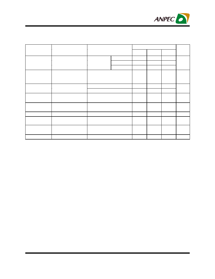
Electrical Characteristics (Cont.)
T
A
= 25∞C ( unless otherwise noted)
APL431
Symbol
Parameter
Test Conditions
Min.
Typ.
Max.
Unit
APL431A
2.487
2.500
2.513
APL431B
2.475
2.500
2.525
V
REF
Reference voltage
V
KA
=V
REF
,
I
K
=10mA*
1
APL431C
2.450
2.500
2.550
V
V
REF
/ T
Reference voltage
drift over temp. range
V
KA
=V
REF
,I
K
=10mA
T
A
=0 to 70∞C*
1
T
A
=-40 to 85∞C*
1
20
30
mV
I
K
=10mA, V
KA
=V
REF
to 10V
*2
-1.5
-3
V
REF
/
V
KA
Voltage ratio (open
loop gain)
I
K
=10mA, V
KA
=V
REF
to 20V
*2
-1.2
-2.5
mV/V
I
REF
Reference current
I
K
=10mA,
R
1
=10k, R
2
=open
*2
1.0
3
µA
I
REF
/T
Reference current
drift
I
K
=10mA, R
1
=10k
,
R
2
=open, T
A
= -40 to 85
∞C
*2
0.3
1
µA
I
K(min)
Min. cathode current V
KA
=V
REF
*1
0.25
0.5
mA
I
K(off)
Off-state cathode
current
V
KA
= 20V, V
REF
= 0V
*3
0.1
1
µA
|Z
KA
|
Dynamic impedance
V
KA
=V
REF
I
K
=1mA to 100mA, f
1kHz
*1
0.1
0.4
I
K
Cathode current
V
KA
=V
REF
+ 50mV
*2
100
mA
Notes :
*1 : use Figure 1
*2 : use Figure 2
*3 : use Figure 3

Copyright ANPEC Electronics Corp.
Rev. C.1 - Jun., 2003
APL431
www.anpec.com.tw
4
Test figures
Figure 1. Test Circuit for V
KA
=V
REF
, V
O
=V
KA
=V
REF
Figure 2. Test Circuit for V
KA
>V
REF
,
V
O
= V
KA
= V
REF
◊ (1+R
1
/R
2
) + I
REF
◊ R
1
Figure 3. Test Circuit for I
K(off)
Application schematic
R
b
should provide cathode current large than
1mA to maintain APL431 work properly.
V
IN
V
o
I
K
V
REF
V
o
V
IN
I
K(off)
V
IN
I
K
I
REF
V
REF
R1
R2
V
o
V
o
V
IN
27.5k
0.1%
27.5k
0.1%
R
b
5-Volt Precision Regulator

Copyright ANPEC Electronics Corp.
Rev. C.1 - Jun., 2003
APL431
www.anpec.com.tw
5
2.47
2.475
2.48
2.485
2.49
2.495
2.5
2.505
2.51
2.515
2.52
-20
0
20
40
60
80
100
-40
-200
0
200
400
600
800
-1
0
1
2
3
0
-2 00
2 0 0
4 0 0
6 0 0
8 0 0
-1
0
1
2
3
Typical Characteristics
Cathode Current (
µ
A)
Cathode Current vs. Cathode Voltage
Cathode Voltage (V)
Temperature (∞C)
Reference Voltage vs. Temperature
Reference V
oltage (V)
Temperature (∞C)
Reference Input Current (
µ
A)
Reference Input Current vs. Temperature
Cathode Current vs. Cathode Voltage
Cathode Voltage (V)
Cathode Current (mA)
I
K-MIN
0
0.5
1
1.5
2
-40
-20
0
20
40
60
80
100