Copyright
©
ANPEC Electronics Corp.
Rev. A.2 - Feb., 2006
APW7074
www.anpec.com.tw
1
Features
Applications
General Description
The APW7074 uses fixed 300KHz switching frequency,
voltage mode, synchronous PWM controller which
drives dual N-channel MOSFETs. The device integrates
all of the control, monitoring and protecting functions
into a single package, provides one controlled power
output with under-voltage and over-current protections.
The APW7074 provides excellent regulation for
output load variation. The internal 0.8V temperature-
compensated reference voltage is designed to meet
the requirement of low output voltage applications.
The APW7074 with excellent protection functions:
POR, OCP and UVP. The Power-On-Reset (POR) cir-
cuit can monitor the VCC, EN, and OCSET voltage to
make sure the supply voltage exceeds their
threshold voltage while the controller is running.
The Over-Current Protection (OCP) monitors the out-
put current by using the voltage drop across the upper
and lower MOSFET's R
DS(ON)
. When the output cur-
rent reaches the trip point, the controller will run the
soft-start function until the fault events are removed.
The Under-Voltage Protection (UVP) monitors the volt-
age at FB pin (V
FB
) for short-circuit protection, when
the V
FB
is less 50% V
REF
, the controller will shutdown
the IC directly.
∑
Graphic Cards
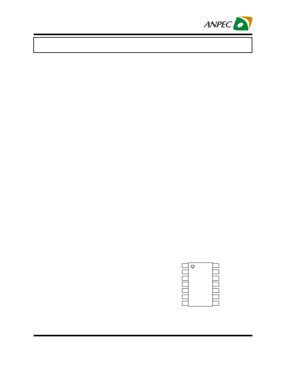
Pin Outs
Synchronous Buck PWM Controller
∑
Single 12V Power Supply Required
∑
0.8V Reference with 1% Accuracy
∑
Shutdown and Soft-start Function
∑
300KHz Fixed Switching Frequency
∑
Voltage Mode PWM Control Design
∑
Up to 100% Duty Cycle
∑
Under-Voltage Protection
∑
Over-Current Protection
∑
SOP-14 Package
∑
Lead Free Available (RoHS Compliant)
1
3
2
4
6
5
7
BOOT
NC
FB
COMP
GND
EN
14
12
13
11
9
10
8
UGA TE
PHASE
OCSET
LGA TE
PGND
V CC
SS
SOP-14
TOP V IEW
PV CC
ANPEC reserves the right to make changes to improve reliability or manufacturability without notice, and
advise customers to obtain the latest version of relevant information to verify before placing orders.

Copyright
©
ANPEC Electronics Corp.
Rev. A.2 - Feb., 2006
APW7074
www.anpec.com.tw
2
Ordering and Marking Information
Block Diagram
Gate Control
Oscillator
Soft Start
Power-On
Reset
PHASE
LGATE
FB
SS
GND
EN
VCC
OCSET
BOOT
UGATE
PGND
PVCC
I
OCSET
200uA
I
SS
10uA
50%V
REF
O.C.P
Comparator
Error Amp
PWM
Comparator
U.V.P
Comparator
Sawtooth
Wave
:
2
COMP
0.27V
O.C.P
Comparator
V
REF
F
OSC
300KHz
V
CC
APW7074
Handling Code
Temp. Range
Package Code
∞
Lead Free Code
APW7074 K :
APW7074
XXXXX
XXXXX - Date Code
Package Code
K : SOP - 14
Temp. Range
E : -20 to 70 C
Handling Code
TU : Tube
TR : Tape & Reel
Lead Free Code
L : Lead Free Device Blank : Original Device
Note: ANPEC lead-free products contain molding compounds/die attach materials and 100% matte tin plate
termination finish; which are fully compliant with RoHS and compatible with both SnPb and lead-free soldering
operations. ANPEC lead-free products meet or exceed the lead-free requirements of IPC/JEDEC J STD-020C for
MSL classification at lead-free peak reflow temperature.

Copyright
©
ANPEC Electronics Corp.
Rev. A.2 - Feb., 2006
APW7074
www.anpec.com.tw
3
Symbol
Parameter
Rating
Unit
VCC, PVCC
VCC, PVCC to GND
-0.3 to +16
V
BOOT
BOOT to PHASE
-0.3 to +16
V
UGATE
UGATE to PHASE <400ns pulse width
>400ns pulse width
-5 to BOOT+5
-0.3 to BOOT +0.3
V
LGATE
LGATE to PGND <400ns pulse width
>400ns pulse width
-5 to PVCC+5
-0.3 to BOOT +0.3
V
PHASE
PHASE to GND <400ns pulse width
>400ns pulse width
-5 to +21
-0.3 to 16
V
OCSET
OCSET to GND
VCC+0.3
V
FB, COMP
FB, COMP to GND
-0.3 to 7
V
PGND
PGND to GND
-0.3 to +0.3
V
T
J
Junction Temperature Range
-20 to +150
∞
C
T
STG
Storage Temperature
-65 ~ 150
∞
C
T
SDR
Soldering Temperature (10 Seconds)
300
∞
C
V
ESD
Minimum ESD Rating
±
2
KV
Absolute Maximum Ratings
Symbol
Parameter
Rating
Unit
VCC, PVCC
IC Supply Voltage
10.8 to 13.2
V
V
IN
Converter Input Voltage
2.2 to 13.2
V
V
OUT
Converter Output Voltage
0.8 to 5
V
I
OUT
Converter Output Current
0 to 25
A
T
A
Ambient Temperature Range
-20 to 70
∞
C
T
J
Junction Temperature Range
-20 to 125
∞
C
Recommended Operating Conditions
Unless otherwise specified, these specifications apply over VCC=12V, and T
A
=-20~70
∞
C. Typical values are at
T
A
=25
∞
C.
Electrical Characteristics
APW7074
Symbol
Parameter
Test Conditions
Min
Typ Max
Unit
INPUT SUPPLY CURRENT
VCC Supply Current
(Shutdown mode)
UGATE, LGATE and EN = GND
0.5
1
mA
I
CC
VCC Supply Current
UGATE and LGATE Open
5
10
mA
Note 1: Absolute Maximum Ratings are those values beyond which the life of a device may be impaired. Exposure to
absolute maximum rating conditions for extended periods may affect device reliability.
Copyright
©
ANPEC Electronics Corp.
Rev. A.2 - Feb., 2006
APW7074
www.anpec.com.tw
4
Unless otherwise specified, these specifications apply over VCC=12V, and T
A
=-20~70
∞
C. Typical values are at
T
A
=25
∞
C.
Electrical Characteristics (Cont.)
APW7074
Symbol
Parameter
Test Conditions
Min
Typ Max
Unit
POWER-ON RESET
Rising VCC Threshold
9
9.5
10.0
V
Falling VCC Threshold
7.5
8
8.5
V
Rising V
OCSET
Threshold
1.3
V
V
OCSET
Hysteresis Voltage
0.1
V
Rising EN threshold Voltage
1.3
V
EN Hysteresis Voltage
0.1
V
OSCILLATOR
F
OSC
Oscillator Frequency
255
300
345
kHz
V
OSC
Ramp Amplitude
(nominal 1.35V to 2.95V)
1.6
V
Duty Duty Cycle Range
0
100
%
REFERENCE
V
REF
Reference Voltage
0.80
V
Reference Voltage Tolerance
-1
+1
%
PWM ERROR AMPLIFIER
Gain Open Loop Gain
R
L
= 10k, C
L
= 10pF (Note3)
88
dB
GBWP Open Loop Bandwidth
R
L
= 10k, C
L
= 10pF (Note3)
15
MHz
SR
Slew Rate
R
L
= 10k, C
L
= 10pF (Note3)
6
V/us
FB Input Current
V
FB
= 0.8V
0.1
1
uA
V
COPM
COMP High Voltage
5.5
V
V
COPM
COMP Low Voltage
0
V
I
COMP
COMP Source Current
V
COMP
= 2V
5
mA
I
COMP
COMP Sink Current
V
COMP
= 2V
5
mA
GATE DRIVERS
I
UGATE
Upper Gate Source Current
BOOT = 12V, V
UGATE
-V
PHASE
= 2V
2.6
A
I
UGATE
Upper Gate Sink Current
BOOT = 12V, V
UGATE
-V
PHASE
= 2V
1.05
A
I
LGATE
Lower Gate Source Current
PVCC = 12V, V
LGATE
= 2V
4.9
A
I
LGATE
Lower Gate Sink Current
PVCC = 12V, V
LGATE
= 2V
1.4
A
R
UGATE
Upper Gate Source Impedance BOOT = 12V, I
UGATE
= 0.1A
2
3
R
UGATE
Upper Gate Sink Impedance
BOOT = 12V, I
UGATE
= 0.1A
1.6
2.4

Copyright
©
ANPEC Electronics Corp.
Rev. A.2 - Feb., 2006
APW7074
www.anpec.com.tw
5
Electrical Characteristics (Cont.)
APW7074
Symbol
Parameter
Test Conditions
Min Typ Max
Unit
GATE DRIVERS (Cont.)
R
LGATE
Lower Gate Source Impedance
PVCC = 12V, I
LGATE
= 0.1A
1.3 1.95
R
LGATE
Lower Gate Sink Impedance
PVCC = 12V, I
LGATE
= 0.1A
1.25 1.88
T
D
Dead Time
20
nS
PROTECTION
UV
FB
FB Under Voltage Level
Percent of V
REF
45
50
55
%
I
OCSET
OCSET Source Current (Hi-Side) V
OCSET
= 11.5V
150 200 250
uA
V
OCP
OCP Voltage (Low-Side)
230 270 310
mV
SOFT START
I
SS
Soft-Start Charge Current
8
10
12
uA
Unless otherwise specified, these specifications apply over VCC=12V, and T
A
=-20~70
∞
C. Typical values are
at T
A
=25
∞
C.
Typical Application Circuit
VCC
BOOT
UGATE
PHASE
PVCC
LGATE
PGND
GND
OCSET
FB
SS
EN
V
OUT
12V
V
IN
ON
OFF
COMP
2.37K
1nF
0.1uF
APM2509
APM2506
1uF
22nF
1uF
SCD24
1N4148
1uH
470uF
2.2uH
470uFx2
1000uFx2
2K
1K
1.5nF
7.5R
18R
68nF
8.2nF
33nF
2.7K
Note 3:Guaranteed by design.