
Copyright
©
ANPEC Electronics Corp.
Rev. A.5 - Aug., 2005
APW7075
www.anpec.com.tw
1
ANPEC reserves the right to make changes to improve reliability or manufacturability without notice, and advise
customers to obtain the latest version of relevant information to verify before placing orders.
Step-Up Converter and LDO Combo
Features
General Description
Applications
∑
Dual Mode Power System
∑
USB Peripheral
∑
Camcorders and Digital Camera
∑
Hand-held Instrument
∑
PDAs
The APW7075 is a PWM/PFM, high-efficiency and
step-up DC-DC converter with an integrated LDO input
switch for dual mode application. During battery mode
operation, the APW7075 acts as synchronous recti-
fier and step-up DC-DC converter with a fixed or ad-
justable output voltage. When the VIN pin sense 5V
input voltage, the APW7075 is switched to LDO op-
eration mode, maintaining the constant output voltage.
The input voltage ranges from 0.6 V to 4.5V for step-
up DC-DC converter. The start-up is guaranteed at1V
and the device is operating down to 0.6V. When the
device is at LDO operating mode, the suitable output
voltage 3.3V and loading current 500mA for maximum
power consumption are guaranteed.
The APW7075 is suited for dual mode and portable
battery powered appliance with low-battery detector.
In dual-mode applications, the APW7075 draws power
from any available 5V USB connection and reverts to
battery power when the USB power is removed.
∑
Built-In a 500mA LDO and Synchronous Step-Up
DC-DC Converter
∑
Built-In PWM/PFM Operating Mode
∑
Provided Dual Input Power Sources
∑
Connect FB to OUT for 3.3V Output Voltage or
GND for 2.5V Output Voltage or an External
Resistor Divider for Adjustable Output Voltage.
∑
Fixed 300KHz Operating Frequency
∑
High Efficiency Up to 94% at 200mA Output
Current
∑
0.6V to 4.5V Operating Voltage
∑
1V Start Up Input Voltage
∑
Low Battery Voltage Detection
∑
Reverse Voltage Protection
∑
Internal Synchronous Rectifier
∑
Automatic Detection Input Voltage
∑
Compact SOP-8-P and TSSOP-8 Packages
∑
Lead Free Available (RoHS Compliant)
Pin Description
VIN
SHDN
FB
LBI
LBO
GND
LX
OUT
1
2
3
4
5
6
7
8
VIN
SHDN
FB
LBI
LBO
GND
LX
OUT
1
2
3
4
5
6
7
8
= Thermal Pad
(connected to GND plane for better heat
dissipation)
TSSOP-8 Top View
SOP-8-P Top View
Copyright
©
ANPEC Electronics Corp.
Rev. A.5 - Aug., 2005
APW7075
www.anpec.com.tw
2
APW7075
Package Code
KA : SOP-8-P O : TSSOP-8
Temp. Range
C : 0 to 70 C
Handling Code
TU : Tube TR : Tape & Reel
Lead Free Code
L : Lead Free Device Blank : Original Device
∞
Handling Code
Temp. Range
Package Code
APW7075 KA :
APW7075
XXXXX
XXXXX - Date Code
APW7075
XXXXX
APW7075 O :
XXXXX - Date Code
Lead Free Code
Ordering and Marking Information
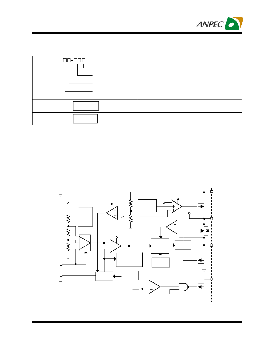
Block Diagram
Drive
Current
Limit
P-MOS
N-MOS
PWM/
PFM
controller
Vref
phase
compensation
soft-start
voltage
reference
Oscillator
Vref
LX
Vref
OUT
VIN
LBO
LBI
FB
GND
P-MOS
SHDN
VDD
VDD
VDD
VDD
N-MOS
Q1
Q2
Q3
Q4
VDD
A
B
C
Y
A
B
C
Y
FB
VOUT
GND
R1,R2
2
SHDN
Note
:
ANPEC lead-free products contain molding compounds/die attach materials and 100% matte tin plate
termination finish; which are fully compliant with RoHS and compatible with both SnPb and lead-free soldiering
operations. ANPEC lead-free products meet or exceed the lead-free requirements of IPC/JEDEC J STD-020C
for MSL classification at lead-free peak reflow temperature.

Copyright
©
ANPEC Electronics Corp.
Rev. A.5 - Aug., 2005
APW7075
www.anpec.com.tw
3
Symbol
Parameter
Value
Unit
R
JA
Thermal Resistance
-
Junction to Ambient
SOP-8
SOP-8-P
TSSOP-8
124
80
160
∞
C/W
Electrical Characteristics
V
BAT
= 2V, FB = OUT (V
OUT
= 3.3V), R
L
=
, T
A
= 0∞C to +85∞C, unless otherwise noted. Typical values are at
T
A
= +25∞C.
APW7075
Symbol
Parameter
Test Conditions
Min.
Typ.
Max.
Unit
Step-up section
V
BAT
Minimum Operating Input
Voltage (Note1)
0.6
V
Operating Voltage
0.6
4.5
V
Start-up Voltage
R
L
= 3K
0.9
1
V
F
SW
Operating Frequency
V
OUT
= 3.3VX96%
300
kHz
D
MAX
Maximum PWM Duty Cycle
V
OUT
= 3.3VX96%
90
%
Power MOSFET
R
DS(on)
-N Active Switch ON Resistance I
LX
= 100mA
0.3
0.6
R
DS(ON)
-P
Synchronous Switch on
Resistance
I
LX
= 100mA
0.6
0.9
Control
FB = OUT, I
LOAD
= 0mA
3.234
3.3
3.366
V
Output Voltage
FB = GND, I
LOAD
= 0mA
2.45
2.5
2.55
V
V
OUT
Output Voltage Range
External divider
2.5
5.5
V
V
OUT(drop)
V
OUT
Dropping Voltage (Note 2) V
OUT
= 3.3V, C
OUT
= 100
µ
F
150
mV
Thermal Characteristics
Absolute Maximum Ratings
Symbol
Parameter
Value
Unit
V
OUT
Supply voltage(OUT to GND)
-0.3 to 6.0
V
V
IO
Input / output pins
-0.3 to 6.0
V
T
A
Operating Ambient Temperature Range
0 to 85
∞C
T
J
Junction Temperature Range
0 to 150
∞C
T
STG
Storage Temperature Range
-65 to +150
∞C
T
S
Soldering Temperature
300, 10 seconds
∞C

Copyright
©
ANPEC Electronics Corp.
Rev. A.5 - Aug., 2005
APW7075
www.anpec.com.tw
4
Unless otherwise noted these specifications apply over full temperature, 3.9V
VIN<5.5V, C
OUT
10
µ
F,
SHDN=V
IN
,Typical values are at T
A
=+25∞C.)
APW7075
Symbol
Parameter
Test Conditions
Min.
Typ.
Max.
Unit
T
SS
Soft-start Time
V
OUT
= 3.3V
30
100
ms
V
REF
FB Input Threshold
I
LOAD
= 0mA
1.176
1.2
1.224
V
I
FB
FB Input Current
V
FB
= 1.4V
0.03
50
nA
I
DD
Operating Current (Note3) V
OUT
= 3.3VX96%, I
LOAD
= 0mA
70
140
µ
A
Shutdown Current
V
SHDN
= 0
0.1
5
µ
A
I
SHDN
SHDN Input Current
V
SHDN
= 0 or V
OUT
0.07
50
nA
Logic LOW (V
IL
)
0.8
0.3
V
SHDN
Logic HIGH(V
IH
)
1.4
0.8
V
LBI Input Hysteresis
10
mV
V
LBI
LBI Threshold
0.588
0.6
0.612
V
I
LBI
LBI Input Current
V
LBI
= 0.8V
1
50
nA
V
LBO
LBO Logic Low
V
LBI
= 0, I
SINk
= 1mA
0.2
0.4
V
I
LBO
LBO Off Leakage Current V
LBO
= 5.5V, V
LBI
= 5.5V
0.07
1
µ
A
LDO Section (Note4)
V
IN(upper)
Upper V
IN
Threshold
Voltage
V
IN
increasing
3.75
3.9
4.05
V
V
IN(lower)
Lower V
IN
Threshold
Voltage
V
IN
decreasing
3.65
3.8
3.95
V
V
TH
VIN Threshold Hysteresis
100
mV
V
OUT
Output Voltage
V
OUT
-2
V
OUT
V
OUT
+2
V
I
LIM
Current Limit
V
IN
= 5V
1
A
I
SHORT
Short Current
V
OUT
= 0V
110
mA
I
OUT
Load Current
500
mA
V
DROP
Dropout Voltage
I
LOAD
= 500mA
0.6
0.9
V
No load
800
1000
uA
Iq
Quiescent Current
I
LOAD
= 500mA
1.1
1.5
mA
REG
LINE
Line Regulation
4V<V
IN
<5.5V, I
LOAD
= 0mA
4
10
mV
REG
LOAD
Load Regulation
V
IN
= 5V, 0mA<I
LOAD
<500mA
20
30
mV
Note1: The min. operating voltage is dependent on the duty cycle.
Note2: The dropped output voltage is that the input power (VIN pin) is switched to battery power (LX pin),
when the VIN power is removed.
Note3: Device is boostrapped ( power to the IC comes from OUT). This correlates directly with the actual
battery supply.
Note4: If the LDO mode is used, the output voltage should be under 3.8V.
Electrical Characteristics (Cont.)

Copyright
©
ANPEC Electronics Corp.
Rev. A.5 - Aug., 2005
APW7075
www.anpec.com.tw
5
Application Schematic
Connect the R6=500
to 1k
to GND
Figure 1. Dual Model : 3.3V Output Voltage
APW7075
1
VIN
SHDN
LBI
LBO
OUT
LX
GND
FB
2
3
4
8
7
6
5
VBAT
Adapter
5V
C2
100uF
C1
10uF
L1
22UH
ON
OFF
C3
10uF
C4
1uF
VOUT
R3
R4
100k
3.3V
Low Battery Output
1N5817
R6
R5
Pin Function Description
VIN (Pin 1)
Input supply voltage for dual-mode application. Con-
nect a schokkty diode (current rating >500mA) to USB
port or 5V adapter. If the LDO mode is not used, tie
the VIN pin to ground.
FB (pin 2)
Internal 1.2V reference voltage. Connect to OUT for 3.
3V output,. Connect to GND for 2.5V output. Use a
resistor divider to set the output voltage from 2.5V to
5.5V.
SHDN (pin 3)
Shutdown input. High = operating mode; Low = shut-
down mode.
LBI (Pin 4)
Low-battery comparator input. Internally set to trip at
0.6V.
LBO (pin 5)
Open-drain low battery comparator output. Connect
LBO to OUT through a 100K
resistor. Output is low
as V
LBI
< 0.6V. Open-drain device is turned on during
shutdown.
OUT (pin 8)
Power output. OUT provides bootstrap power to the
IC.
GND (Pin 6)
Ground pins of the circuitry and all ground pins must
be soldered to PCB with proper power dissipation.
LX (pin 7)
N-channel and P-channel power MOSFET drain
connection.