APEX MICROTECHNOLOGY CORPORATION ∑ TELEPHONE (520) 690-8600 ∑ FAX (520) 888-3329 ∑ ORDERS (520) 690-8601 ∑ EMAIL prodlit@apexmicrotech.com
1
FEATURES
∑ HIGH VOLTAGE OPERATION -- ±150V (PA82J)
∑ HIGH OUTPUT CURRENT -- ±30mA (PA81J)
∑ LOW BIAS CURRENT, LOW NOISE -- FET Input
APPLICATIONS
∑ HIGH IMPEDANCE BUFFERS UP TO ±140V
∑ ELECTROSTATIC TRANSDUCER & DEFLECTION
∑ PROGRAMMABLE POWER SUPPLIES TO ±145V
∑ BIOCHEMISTRY STIMULATORS
∑ COMPUTER TO VACUUM TUBE INTERFACE
DESCRIPTION
The PA80 series of high voltage operation amplifiers provides
an extremely wide range of supply capability with two over-
lapping products. High accuracy is achieved with a cascode
input circuit configuration. All internal biasing is referenced
to a zener diode. As a result, these models offer outstanding
common mode and power supply rejection. The output stage
operates in the class A/B mode for best linearity. Internal phase
compensation assures stability at all gain settings without
external components. Fixed internal current limits protect
these amplifiers against a short circuit to common at most
supply voltages. For sustained high energy flyback, external
fast recovery diodes should be used. However, a heatsink
may be necessary to maintain the proper case temperature
under normal operating conditions.
This hybrid circuit utilizes thick film resistors, ceramic
capacitors and silicon semiconductors to maximize reliabil-
ity, minimize size and give top performance. Ultrasonically
bonded aluminum wires provide reliable interconnections
at all operating temperatures. The 8-pin TO-3 package (see
Package Outlines) is hermetically sealed and isolated from
the internal circuits. The use of compressible thermal washers
voids the warranty.
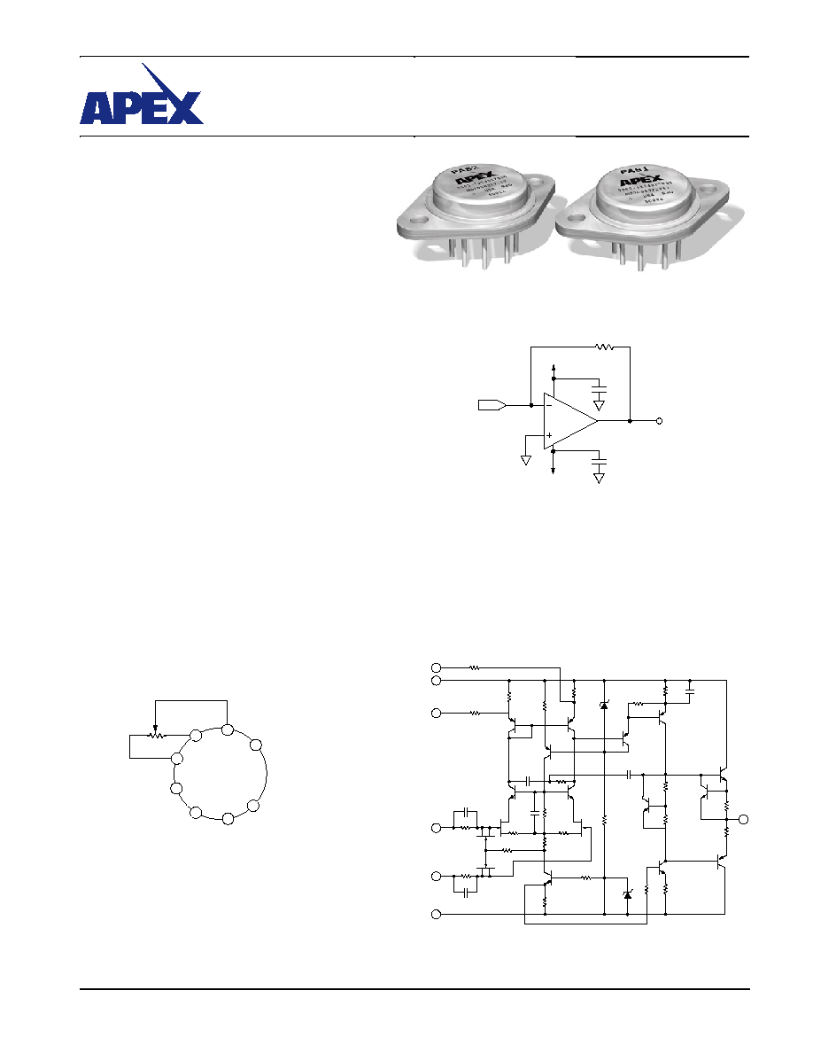
EXTERNAL CONNECTIONS
TYPICAL APPLICATION
The PA81 and 70K ohm resistor form a current to voltage
converter, accepting ±1mA from a 12 bit current output digital
to analog converter. The power op amp contribution to the er-
ror budget is insignificant. At a case temperature of 70∞C, the
combination of voltage offset and bias errors amounts to less
than 31ppm of full scale range. Incorporation of the optional
offset trim can further reduce these errors to under 9ppm.
EQUIVALENT SCHEMATIC
8-PIN TO-3
PACKAGE STYLE CE

APEX MICROTECHNOLOGY CORPORATION ∑ 5980 NORTH SHANNON ROAD ∑ TUCSON, ARIZONA 85741 ∑ USA ∑ APPLICATIONS HOTLINE: 1 (800) 546-2739
2
ABSOLUTE MAXIMUM RATINGS
SPECIFICATIONS
SPECIFICATIONS
ABSOLUTE MAXIMUM RATINGS
PA81J
PA82J
SUPPLY VOLTAGE, +V
S
to ≠V
S
200V
300V
OUTPUT CURRENT, within SOA
Internally Limited
POWER DISSIPATION, internal
11.5W
11.5W
INPUT VOLTAGE, differential
±150V
±300V
INPUT VOLTAGE, common mode
±V
S
±V
S
TEMPERATURE, pin solder - 10 sec
300∞C
300∞C
TEMPERATURE, junction
150∞C
150∞C
TEMPERATURE RANGE, storage
≠65 to +125∞C
≠65 to +125∞C
OPERATING TEMPERATURE RANGE, case
≠55 to +125∞C
≠55 to +125∞C
PA81J
PA82J
PARAMETER
TEST CONDITIONS
2
MIN
TYP
MAX
MIN
TYP
MAX
UNITS
INPUT
OFFSET VOLTAGE, initial
T
C
= 25∞C
±1.5
±3
*
*
mV
OFFSET VOLTAGE, vs. temperature
Full temperature range
10
25
*
*
µV/∞C
OFFSET VOLTAGE, vs. supply
T
C
= 25∞C
20
*
µV/V
OFFSET VOLTAGE, vs. time
T
C
= 25∞C
75
*
µV/kh
BIAS CURRENT, initial
T
C
= 25∞C
5
50
*
*
pA
BIAS CURRENT, vs. supply
T
C
= 25∞C
.2
*
pA/V
OFFSET CURRENT, initial
T
C
= 25∞C
2.5
50
*
*
pA
INPUT IMPEDANCE, DC
T
C
= 25∞C
10
11
*
INPUT CAPACITANCE
T
C
= 25∞C
10
*
pF
COMMON MODE VOLTAGE RANGE
2
Full temperature range
±V
S
≠10
*
V
COMMON MODE REJECTION, DC
V
CM
= ±20V
110
*
dB
GAIN
OPEN LOOP GAIN at 10Hz
Full load
94
116
100
118
dB
UNITY GAIN BANDWIDTH
T
C
= 25∞C
5
*
MHz
POWER BANDWIDTH
T
C
= 25∞C, full load
60
30
kHz
PHASE MARGIN
Full temperature range
45
*
∞
OUTPUT
VOLTAGE SWING
2
T
C
= 25∞C, I
PK
±V
S
≠5
*
V
CURRENT, peak
T
C
= 25∞C
30
15
mA
CURRENT, limit
T
C
= 25∞C
50
25
mA
SETTLING TIME to .1%
T
C
= 25∞C, 10V step
12
*
µs
SLEW RATE
4
T
C
= 25∞C
20
*
V/µs
CAPACITIVE LOAD
A
V
= 1
10
*
nF
POWER SUPPLY
VOLTAGE
Full temperature range
±32
±75
±75
±70
±150
±150
V
CURRENT, quiescent
T
C
= 25∞C
6.5
8.5
6.5
8.5
mA
THERMAL
RESISTANCE, AC, junction to case
3
F > 60Hz
6
*
∞C/W
RESISTANCE, DC, junction to case
3
F < 60Hz
9
10
*
*
∞C/W
RESISTANCE, junction to air
Full temperature range
30
*
∞C/W
TEMPERATURE RANGE, shutdown
150
*
∞C
TEMPERATURE RANGE, case
Meets full range specification
0
70
*
*
∞C
PA81J ∑ PA82J
NOTES: * The specification of PA82J is identical to the specification for PA81J in applicable column to the left.
1. The power supply voltage for all specifications is the TYP rating unless noted as a test condition.
2. +V
S
and ≠V
S
denote the positive and negative supply rail respectively. Total V
S
is measured from +V
S
to ≠V
S
.
3. Rating applies if the output current alternates between both output transistors at a rate faster than 60Hz.
4. On the PA81J and PA82J, signal slew rates at pins 5 and 6 must be limited to less than 1V/ns to avoid damage. When faster
waveforms are unavoidable, resistors in series with those pins, limiting current to 150mA will protect the amplifier from damage.
The internal substrate contains beryllia (BeO). Do not break the seal. If accidentally broken, do not crush, machine, or
subject to temperatures in excess of 850∞C to avoid generating toxic fumes.
CAUTION
APEX MICROTECHNOLOGY CORPORATION ∑ 5980 NORTH SHANNON ROAD ∑ TUCSON, ARIZONA 85741 ∑ USA ∑ APPLICATIONS HOTLINE: 1 (800) 546-2739
4
OPERATING
CONSIDERATIONS
PA81J ∑ PA82J
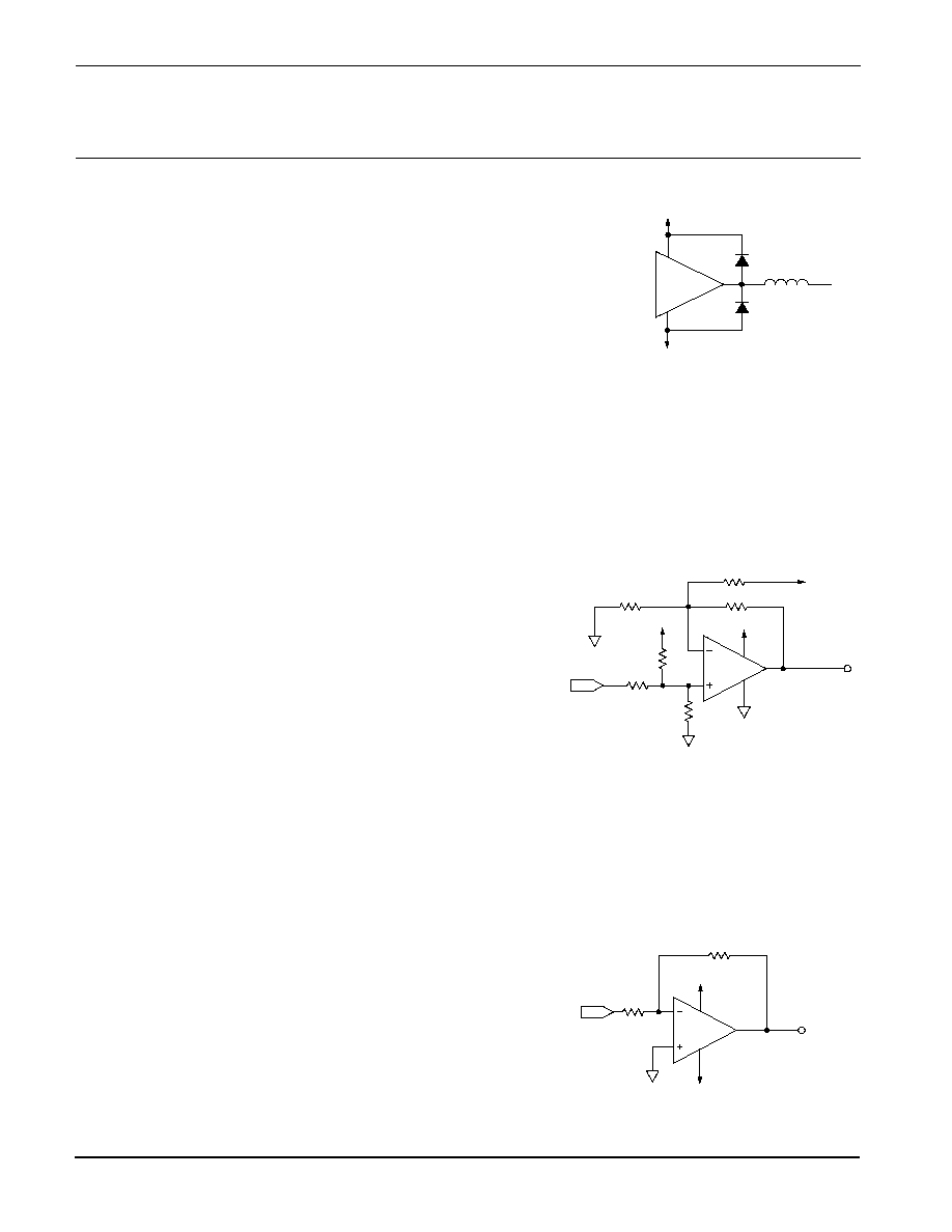
SINGLE SUPPLY OPERATION
These amplifiers are suitable for operation from a single sup-
ply voltage. The operating requirements do however, impose
the limitation that the input voltages do not approach closer
than 10 volts to either supply rail. This is due to the operating
voltage requirements of the current sources, the half-dynamic
loads and the cascode stage. Refer to the simplified schemat-
ics.Thus, single supply operation requires the input signals
to be biased at least 10 volts from either supply rail. Figure 3
illustrates one bias technique to achieve this.
Figure 4 illustrates a very common deviation from true single
supply operation. The availibility of two supplies still allows
ground (common) referenced signals, but also maximizes the
high voltage capability of the unipolar output. This technique
can utilize an existing low voltage system power supply and
does not place large current demands on that supply. The 12
volt supply in this case must supply only the quiescent current
of the PA81J, which is 8.5mA maximum. If the load is reactive
or EMF producing, the low voltage supply must also be able to
absorb the reverse currents generated by the load.
GENERAL
Please read Application Note 1 "General Operating Con-
siderations" which covers stability, supplies, heat sinking,
mounting, current limit, SOA interpretation, and specification
interpretation. Visit www.apexmicrotech.com for design tools
that help automate tasks such as calculations for stability, in-
ternal power dissipation, current limit and heat sink selection.
The "Application Notes" and "Technical Seminar" sections
contain a wealth of information on specific types of applications.
Package outlines, heat sinks, mounting hardware and other
accessories are located in the "Packages and Accessories"
section. Evaluation Kits are available for most Apex product
models, consult the "Evaluation Kit" section for details. For
the most current version of all Apex product data sheets, visit
www.apexmicrotech.com.
SAFE OPERATING AREA (SOA)
For the PA80J and PA81J, the combination of voltage capa-
bility and internal current limits mandate that the devices are
safe for all combinations of supply voltage and load. On the
PA82J, any load combination is safe up to a total supply of 250
volts. When total supply voltage equals 300 volts, the device
will be safe if the output current is limited to 10 milliamps or
less. This means that the PA82J used on supplies up to 125
volts will sustain a short to common or either supply without
danger. When using supplies above ±125 volts, a short to
one of the supplies will be potentially destructive. When us-
ing single supply above 250 volts, a short to common will be
potentially destructive.
Safe supply voltages do not imply disregard for heatsinking.
The thermal calculations and the use of a heatsink are required
in many applications to maintain the case temperature within
the specified operating range of 0 to 70∞C. Exceeding this case
temperature range can result in an inoperative circuit due to
excessive input errors or activation of the thermal shutdown.
INDUCTIVE LOADS
Two external diodes as shown in Figure 2, are required
to protect these amplifiers against flyback (kickback) pulses
exceeding the supply voltage of the amplifier when driving in-
ductive loads. For component selection, these external diodes
must be very quick, such as ultra fast recovery diodes with
no more than 200 nanoseconds of reverse recovery time. Be
sure the diode voltage rating is greater than the total of both
supplies. The diode will turn on to divert the flyback energy
into the supply rails thus protecting the output transistors from
destruction due to reverse bias.
A note of caution about the supply. The energy of the flyback
pulse must be absorbed by the power supply. As a result, a
transient will be superimposed on the supply voltage, the
magnitude of the transient being a function of its transient
impedance and current sinking capability. If the supply voltage
plus transient exceeds the maximum supply rating, or if the
AC impedance of the supply is unknown, it is best to clamp
the output and the supply with a zener diode to absorb the
transient.
This data sheet has been carefully checked and is believed to be reliable, however, no responsibility is assumed for possible inaccuracies or omissions. All specifications are subject to change without notice.
PA81_82JU REV H MARCH 2001 © 2001 Apex Microtechnology Corp.
