APEX MICROTECHNOLOGY CORPORATION ∑ TELEPHONE (520) 690-8600 ∑ FAX (520) 888-3329 ∑ ORDERS (520) 690-8601 ∑ EMAIL prodlit@apexmicrotech.com
SA06
USA
BeO
TE949311
FEATURES
∑ WIDE SUPPLY RANGE--16-500V
∑ 10A CONTINUOUS TO 75
∞
C CASE
∑ 3 PROTECTION CIRCUITS
∑ ANALOG OR DIGITAL INPUTS
∑ SYNCHRONIZED OR EXTERNAL OSCILLATOR
∑ FLEXIBLE FREQUENCY CONTROL
APPLICATIONS
∑ MOTORS
∑ REACTIVE LOADS
∑ LOW FREQUENCY SONAR
∑ LARGE PIEZO ELEMENTS
∑ OFF-LINE DRIVERS
∑ C-D WELD CONTROLLER
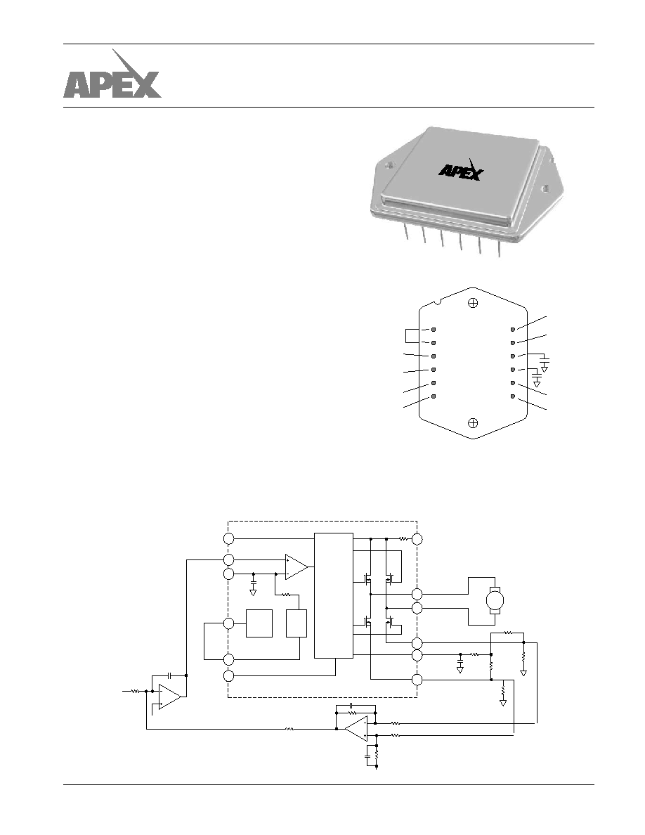
DESCRIPTION
The SA06 is a pulse width modulation amplifier that can
supply 5000W to the load. An internal oscillator requires no
external components. The clock input stage divides the oscil-
lator frequency by two, which provides the switching fre-
quency of 22.5 kHz. External oscillators may also be used to
lower the switching frequency or to synchronize multiple
amplifiers. Current sensing is provided for each half of the
bridge giving amplitude and direction data. A shutdown input
turns off all four drivers of the H bridge output. A high side
current limit and the programmable low side current limit
protect the amplifier from shorts to supply or ground in addition
to load shorts. The H bridge output MOSFETs are protected
from thermal overloads by directly sensing the temperature of
the die. The 12-pin hermetic MO-127/40S power package
occupies only 3 square inches of board space.
BLOCK DIAGRAM AND TYPICAL APPLICATION
MOTOR TORQUE CONTROL
EXTERNAL CONNECTIONS
+V
S
A OUT
B OUT
ILIM/SHDN
I SENSE A
I SENSE B
RSENSE
RSENSE
MOTOR
GND
CLK IN
CONTROL
SIGNAL
CLK OUT
≠PWM/RAMP
+PWM
Vcc
5V
5V
SHUTDOWN
CONTROL
OUTPUT
DRIVERS
PWM
56K
1K
1K
5K
.01
µ
F
470pF
˜
2
OSC
CURRENT
LIMIT
9
8
3
10
4
2
1
5
11
12
6
7
TOP
VIEW
CLK IN
CLK OUT
+PWM
≠PWM/RAMP
GND
ILIM/SHDN
ISENSE A
A OUT
+VS
VCC
*
*
B OUT
I SENSE B
1
2
3
4
5
6
12
11
10
9
8
7
TOP
VIEW
Case tied to pin 5. Allow no current in case. Bypassing of supplies
is required. Package is Apex MO-127/40S. See Outline
Dimensions/Packages in Apex data book.
If +PWM > RAMP/≠PWM then A OUT > B OUT.
*See text.
H T T P : / / W W W . A P E X M I C R O T E C H . C O M ( 8 0 0 ) 5 4 6 - A P E X ( 8 0 0 ) 5 4 6 - 2 7 3 9
M I C R O T E C H N O L O G Y
PULSE WIDTH MODULATION AMPLIFIER
SA06
APEX MICROTECHNOLOGY CORPORATION ∑ 5980 NORTH SHANNON ROAD ∑ TUCSON, ARIZONA 85741 ∑ USA ∑ APPLICATIONS HOTLINE: 1 (800) 546-2739
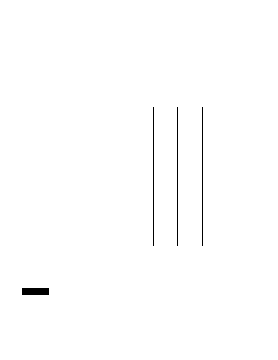
ABSOLUTE MAXIMUM RATINGS
SPECIFICATIONS
SA06
ABSOLUTE MAXIMUM RATINGS
SUPPLY VOLTAGE, +V
S
500V
SUPPLY VOLTAGE, V
CC
16V
POWER DISSIPATION, internal
300W
TEMPERATURE, pin solder - 10s
300
∞
C
TEMPERATURE, junction
2
150
∞
C
TEMPERATURE, storage
≠65 to +150
∞
C
OPERATING TEMPERATURE RANGE, case
≠55 to +125
∞
C
INPUT VOLTAGE, +PWM
0 to +11V
INPUT VOLTAGE, ≠PWM
0 to +11V
INPUT VOLTAGE, I
LIM
0 to +10V
The SA06 is constructed from MOSFET transistors. ESD handling procedures must be observed.
The internal substrate contains beryllia (BeO). Do not break the seal. If accidentally broken, do not crush,
machine, or subject to temperatures in excess of 850
∞
C to avoid generating toxic fumes.
CAUTION
NOTES: 1.
Each of the two active output transistors can dissipate 150W.
2.
Unless otherwise noted: T
C
= 25
∞
C, V
S
, V
CC
at typical specification.
3.
Long term operation at the maximum junction temperature will result in reduced product life. Derate internal power
dissipation to achieve high MTTF. For guidance, refer to the heatsink data sheet.
4.
Guaranteed but not tested.
5.
If 100% duty cycle is not required V
S(MIN)
= 0V.
SPECIFICATIONS
PARAMETER
TEST CONDITIONS
2
MIN
TYP
MAX
UNITS
CLOCK (CLK)
CLK OUT, high level
4
I
OUT
1mA
4.8
5.3
V
CLK OUT, low level
4
I
OUT
1mA
0
.4
V
FREQUENCY
44.10
45.00
46.90
kHz
RAMP, center voltage
5
V
RAMP, P-P voltage
4
V
CLK IN, low level
4
0
.9
V
CLK IN, high level
4
3.7
5.4
V
OUTPUT
TOTAL R
ON
.95
EFFICIENCY, 10A output
V
S
= 500V
97
%
SWITCHING FREQUENCY
OSC in
˜
2
22.05
22.50
22.95
kHz
CURRENT, continuous
4
75
∞
C case
10
A
CURRENT, peak
4
15
A
POWER SUPPLY
VOLTAGE, V
S
Full temperature range
16
5
240
500
V
VOLTAGE, V
CC
Full temperature range
14
15
16
V
CURRENT, V
CC
I
OUT
= 0
80
mA
CURRENT, V
CC,
shutdown
50
mA
CURRENT, V
S
No Load
90
mA
I
LIM
/SHUTDOWN
TRIP POINT
90
110
mV
INPUT CURRENT
100
nA
THERMAL
3
RESISTANCE, junction to case
Full temperature range, for each die
.83
∞
C/W
RESISTANCE, junction to air
Full temperature range
12
∞
C/W
TEMPERATURE RANGE, case
Meets full range specifications
≠25
+85
∞
C
APEX MICROTECHNOLOGY CORPORATION ∑ TELEPHONE (520) 690-8600 ∑ FAX (520) 888-3329 ∑ ORDERS (520) 690-8601 ∑ EMAIL prodlit@apexmicrotech.com
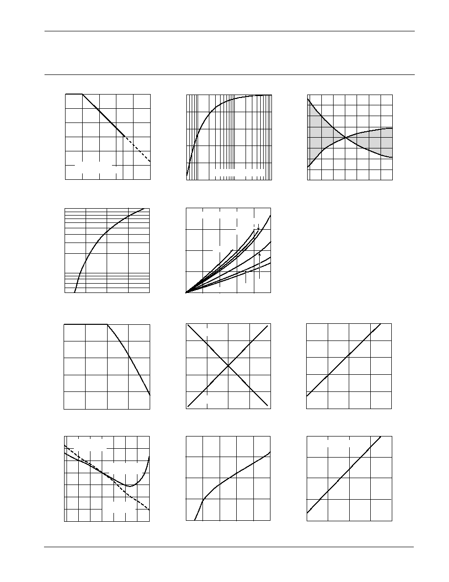
TYPICAL PERFORMANCE
GRAPHS
SA06
≠50
CASE TEMPERATURE, (
∞
C)
CLOCK FREQUENCY OVER TEMP
NORMALIZED FREQUENCY, (%)
≠25
0
25
50
75 100 125
98.0
98.5
99.0
99.5
100
100.5
101.0
101.5
102.0
≠50 ≠25
0
25
50
75
100 125
80
85
90
95
100
105
110
115
Vcc QUIESCENT CURRENT
NORMALIZED Vcc QUIESCENT CURRENT, (%)
1M
100K
95
98
99
100
CLOCK LOADING
96
97
10K
NORMALIZED FREQUENCY, (%)
CASE TEMPERATURE, (
∞
C)
CLOCK LOAD RESISTANCE, (
)
0.6
SOURCE TO DRAIN DIODE VOLTAGE
REVERSE DIODE
FLYBACK CURRENT, Isd (A)
25
50
75
100
125
7
8
9
10
CONTINUOUS OUTPUT
6
0.8
1.0
1.2
1.4
5
0
100
200
300
400
500
25
10
15
20
CASE TEMPERATURE, (
∞
C)
CONTINUOUS AMPS
5
0
75
100
CASE TEMPERATURE, (
∞
C)
0
POWER DERATING
150
25
DUTY CYCLE VS ANALOG INPUT
DUTY CYCLE, (%)
50
125
25
50
75
100
125
0
20
40
60
80
100
INTERNAL POWER DISSIPATION, (W)
ANALOG INPUT, (V)
3
5
4
7
6
SWITCHING FREQUENCY, F (kHz)
Vs, (V)
75
80
85
90
100
95
Vcc QUIESCENT CURRENT
NORMALIZED Vcc QUIESCENT CURRENT, (%)
60
80
100
120
140
Vs QUIESCENT VS VOLTAGE
5
25
SWITCHING FREQUENCY, F (kHz)
40
20
60
80
Vs QUIESCENT VS FREQUENCY
NORMALIZED Vs QUIESCENT CURRENT, (%)
NORMALIZED Vs QUIESCENT CURRENT, (%)
100
10
15
20
A OUT
B OUT
EACH ACTIVE
OUTPUT TRANSISTOR
F NOMINAL = 45kHz
Vcc = 15V
F = 22.5 kHz
NORMAL
OPERATION
SHUTDOWN
OPERATION
Vs = 250V, NO LOAD
0
2
4
6
8
10
OUTPUT CURRENT, (A)
0
5
10
15
20
TOTAL VOLTAGE DROP
TOTAL VOLTAGE DROP, (V)
125
∞
C
100
∞
C
85
∞
C
75
∞
C
25
∞
C
≠25
∞
C
≠55
∞
C
CASE TEMPERATURE
10
1

Switching noise spikes will
invariably be found at the I
SENSE pins. The noise spikes
could trip the current limit thresh-
old which is only 100 mV. R
FILTER
and C
FILTER
should be adjusted
so as to reduce the switching
noise well below 100 mV to
prevent false cur-
rent limiting. The
sum of the DC
level plus the
noise peak will
determine the
current limiting
value. As in most
switching circuits
it may be difficult to determine the true noise amplitude without
careful attention to grounding of the oscilloscope probe. Use
the shortest possible ground lead for the probe and connect
exactly at the GND terminal of the amplifier. Suggested start-
ing values are C
FILTER
= .01uF, R
FILTER
= 5k .
The required value of R
LIMIT
in voltage mode may be calcu-
lated by:
R
LIMIT
= .1 V / I
LIMIT
where R
LIMIT
is the required resistor value, and I
LIMIT
is the
maximum desired current. In current mode the required value
of each R
LIMIT
is 2 times this value since the sense voltage is
divided down by 2 (see Figure B). If R
SHDN
is used it will further
divide down the sense voltage. The shutdown divider network
will also have an effect on the filtering circuit.
BYPASSING
Adequate bypassing of the power supplies is required for
proper operation. Failure to do so can cause erratic and low
efficiency operation as well as excessive ringing at the outputs.
The Vs supply should be bypassed with at least a 1
µ
F ceramic
capacitor in parallel with another low ESR capacitor of at least
10
µ
F per amp of output current. Capacitor types rated for
switching applications are the only types that should be consid-
ered. The bypass capacitors must be physically connected
directly to the power supply pins. Even one inch of lead length
will cause excessive ringing at the outputs. This is due to the
very fast switching times and the inductance of the lead
connection. The bypassing requirements of the Vcc supply are
less stringent, but still necessary. A .1
µ
F to .47
µ
F ceramic
capacitor connected directly to the Vcc pin will suffice.
STARTUP CONDITIONS
The high side of the all N channel output bridge circuit is
driven by bootstrap circuit and charge pump arrangement. In
order for the circuit to produce a 100% duty cycle indefinitely
the low side of each half bridge circuit must have previously
been in the ON condition. This means, in turn, that if the input
signal to the SA06 at startup is demanding a 100% duty cycle,
the output may not follow the command and may be in a tri-
state condition. The ramp signal must cross the input signal at
some point to correctly determine the output state. After the
ramp crosses the input signal level one time, the output state
will be correct thereafter.
I SENSE A
I SENSE B
I LIMIT/SHDN
R
FILTER
C
FILTER
R
LIMIT
R
SHDN
SHUTDOWN
SIGNAL
1K
FIGURE A. CURRENT LIMIT WITH
SHUTDOWN VOLTAGE MODE.
I SENSE A
I SENSE B
I LIMIT/SHDN
R
FILTER
C
FILTER
R
SHDN
SHUTDOWN
SIGNAL
1K
FIGURE B. CURRENT LIMIT WITH
SHUTDOWN CURRENT MODE.
R
LIMIT
R
LIMIT
OPERATING
CONSIDERATIONS
SA06
GENERAL
Please read Application Note 30 on "PWM Basics". Refer to
Application Note 1 "General Operating Considerations" for
helpful information regarding power supplies, heat sinking and
mounting. Visit www.apexmicrotech.com for design tools that
help automate pwm filter design; heat sink selection; Apex's
complete Application Notes library; Technical Seminar Work-
book; and Evaluation Kits.
CLOCK CIRCUIT AND RAMP GENERATOR
The clock frequency is internally set to a frequency of
approximately 45kHz. The CLK OUT pin will normally be tied
to the CLK IN pin. The clock is divided by two and applied to an
RC network which produces a ramp signal at the ≠PWM/
RAMP pin. An external clock signal can be applied to the CLK
IN pin for synchronization purposes. If a clock frequency lower
than 45kHz is chosen an external capacitor must be tied to the
≠PWM/RAMP pin. This capacitor, which parallels an internal
capacitor, must be selected so that the ramp oscillates 4 volts
p-p with the lower peak 3 volts above ground.
PWM INPUTS
The full bridge driver may be accessed via the pwm input
comparator. When +PWM > -PWM then A OUT > B OUT. A
motion control processor which generates the pwm signal can
drive these pins with signals referenced to GND.
PROTECTION CIRCUITS
In addition to the externally programmable current limit there
is also a fixed internal current limit which senses only the high
side current. It is nominally set to 140% of the continuous rated
output current. Should either of the outputs be shorted to
ground the high side current limit will latch off the output
transistors. Also, the temperature of the output transistors is
continually monitored. Should a fault condition occur which
raises the temperature of the output transistors to 165
∞
C the
thermal protection circuit will activate and also latch off the
output transistors. In either case, it will be necessary to remove
the fault condition and recycle power to V
CC
to restart the circuit.
CURRENT LIMIT
There are two load current sensing pins, I SENSE A and I
SENSE B. The two pins can be shorted in the voltage mode
connection but both must be used in the current mode connec-
tion (see figures A and B). It is recommended that R
LIMIT
resistors be non-inductive. Load current flows in the I SENSE
pins. To avoid errors
due to lead lengths
connect the I LIMIT/
SHDN pin directly to
the R
LIMIT
resistors
(through the filter net-
work and shutdown di-
vider resistor) and con-
nect the R
LIMIT
resis-
tors directly to the GND
pin.
This data sheet has been carefully checked and is believed to be reliable, however, no responsibility is assumed for possible inaccuracies or omissions. All specifications are subject to change without notice.
SA06U REV. F MARCH 2001
© 2001 Apex Microtechnology Corp.