 | –≠–ª–µ–∫—Ç—Ä–æ–Ω–Ω—ã–π –∫–æ–º–ø–æ–Ω–µ–Ω—Ç: ARM1022E | –°–∫–∞—á–∞—Ç—å:  PDF PDF  ZIP ZIP |
Document Outline
- ARM1022Eí
- Change history
- Contents
- List of Tables
- List of Figures
- Preface
- Introduction
- Integer Core
- System Control Coprocessor
- 3.1 About the system control coprocessor
- 3.2 Register descriptions
- 3.2.1 CP15 R0, device ID and cache type registers
- 3.2.2 CP15 R1, control register 1
- 3.2.3 CP15 R2, translation table base register
- 3.2.4 CP15 R3, domain access control register
- 3.2.5 CP15 R4
- 3.2.6 CP15 R5, fault status register
- 3.2.7 CP15 R6, fault address register
- 3.2.8 CP15 R7, index and VA cache operations registers
- 3.2.9 CP15 R8, TLB operations register
- 3.2.10 CP15 R9, cache lockdown register
- 3.2.11 CP15 R10, TLB lockdown register
- 3.2.12 CP15 R11
- 3.2.13 CP15 R12
- 3.2.14 CP15 R13, process ID and context ID registers
- 3.2.15 CP15 R14
- 3.2.16 CP15 R15
- Memory Management Units
- Caches and Write Buffer
- Prefetch Unit
- Bus Interface
- Coprocessor Interface
- JTAG Interface
- Debug
- Instruction Cycle Summary and Interlocks
- Design for Test
- Power Manager
- Clock Generator
- Signal Descriptions
- Glossary
- Index

Copyright © 2001 ARM Limited. All rights reserved.
ARM DDI 0237A
ARM1022ETM
Technical Reference Manual

ii
Copyright © 2001 ARM Limited. All rights reserved.
ARM DDI 0237A
ARM1022ETM
Technical Reference Manual
Copyright © 2001 ARM Limited. All rights reserved.
Release Information
Proprietary Notice
Words and logos marked with
Æ
or
TM
are registered trademarks or trademarks owned by ARM Limited, except
as otherwise stated below in this proprietary notice. Other brands and names mentioned herein may be the
trademarks of their respective owners.
Neither the whole nor any part of the information contained in, or the product described in, this document
may be adapted or reproduced in any material form except with the prior written permission of the copyright
holder.
The product described in this document is subject to continuous developments and improvements. All
particulars of the product and its use contained in this document are given by ARM in good faith. However,
all warranties implied or expressed, including but not limited to implied warranties of merchantability, or
fitness for purpose, are excluded.
This document is intended only to assist the reader in the use of the product. ARM Limited shall not be liable
for any loss or damage arising from the use of any information in this document, or any error or omission in
such information, or any incorrect use of the product.
Confidentiality Status
This document is Open Access. This document has no restriction on distribution.
Product Status
The information in this document is Final (information on a developed product).
Web Address
http://www.arm.com
Change history
Date
Issue
Change
30 Nov, 2001
A
First release

ARM DDI 0237A
Copyright © 2001 ARM Limited. All rights reserved.
iii
Contents
ARM1022E Technical Reference Manual
Preface
About this document .................................................................................. xviii
Feedback .................................................................................................... xxii
Chapter 1
Introduction
1.1
About the processor .................................................................................... 1-2
1.2
Programmer's model ................................................................................... 1-4
1.3
Components of the processor ..................................................................... 1-5
1.4
Instruction set summary ............................................................................ 1-10
Chapter 2
Integer Core
2.1
About the integer core ................................................................................. 2-2
2.2
Pipeline ....................................................................................................... 2-4
2.3
Prefetch unit ................................................................................................ 2-5
2.4
Typical operations ....................................................................................... 2-6
2.5
Load/store unit ............................................................................................ 2-9
2.6
Instruction progression .............................................................................. 2-10
Chapter 3
System Control Coprocessor
3.1
About the system control coprocessor ........................................................ 3-2
3.2
Register descriptions .................................................................................. 3-6

Contents
iv
Copyright © 2001 ARM Limited. All rights reserved.
ARM DDI 0237A
Chapter 4
Memory Management Units
4.1
About the MMUs ......................................................................................... 4-2
4.2
MMU software-accessible registers ............................................................ 4-3
4.3
Address translation ..................................................................................... 4-5
4.4
MMU memory access control ................................................................... 4-21
4.5
MMU cachable and bufferable information ............................................... 4-23
4.6
MMU and write buffer ............................................................................... 4-24
4.7
MMU aborts .............................................................................................. 4-25
4.8
MMU fault checking sequence ................................................................. 4-26
4.9
CPU aborts on MMU faults ....................................................................... 4-29
4.10
Fault priority .............................................................................................. 4-30
4.11
External aborts ......................................................................................... 4-31
4.12
Interaction of the MMU, caches, and write buffer ..................................... 4-33
4.13
Soft page table support ............................................................................ 4-34
Chapter 5
Caches and Write Buffer
5.1
About the caches and write buffer .............................................................. 5-2
5.2
ICache ........................................................................................................ 5-3
5.3
DCache and write buffer ............................................................................. 5-7
5.4
Cache coherence ..................................................................................... 5-16
5.5
Portability issues ....................................................................................... 5-18
Chapter 6
Prefetch Unit
6.1
About the prefetch unit ............................................................................... 6-2
6.2
Branch prediction activity ............................................................................ 6-3
6.3
Branch instruction cycle summary .............................................................. 6-6
6.4
Instruction memory barriers ........................................................................ 6-8
Chapter 7
Bus Interface
7.1
Bus features ............................................................................................... 7-2
7.2
AMBA AHB signals ..................................................................................... 7-3
7.3
Arbiter signals ............................................................................................. 7-6
7.4
AHB control signals .................................................................................... 7-7
7.5
Timing ......................................................................................................... 7-9
7.6
Bus interface ............................................................................................. 7-10
Chapter 8
Coprocessor Interface
8.1
About the coprocessor interface ................................................................. 8-2
8.2
Coprocessor interface signals .................................................................... 8-3
8.3
Design considerations ................................................................................ 8-5
8.4
Parallel execution ....................................................................................... 8-7
8.5
Rules for the interface ................................................................................ 8-8
8.6
Pipeline signal assertion ............................................................................. 8-9
8.7
Instruction issue ........................................................................................ 8-10
8.8
Hold signals .............................................................................................. 8-18
8.9
Instruction cancelation .............................................................................. 8-37

Contents
ARM DDI 0237A
Copyright © 2001 ARM Limited. All rights reserved.
v
8.10
Bounced instructions ................................................................................. 8-44
8.11
Data buses ................................................................................................ 8-49
Chapter 9
JTAG Interface
9.1
JTAG interface and halt mode .................................................................... 9-2
9.2
JTAG instructions ........................................................................................ 9-4
9.3
Scan chain descriptions .............................................................................. 9-8
Chapter 10
Debug
10.1
About the debug unit ................................................................................. 10-2
10.2
Register descriptions ................................................................................ 10-5
10.3
Software lockout function ........................................................................ 10-15
10.4
Halt mode ................................................................................................ 10-16
10.5
Monitor mode .......................................................................................... 10-19
10.6
Values in the link register after aborts ..................................................... 10-20
10.7
Comms channel ...................................................................................... 10-21
Chapter 11
Instruction Cycle Summary and Interlocks
11.1
Cycle timing considerations ...................................................................... 11-2
11.2
Instruction cycle counts ............................................................................. 11-3
11.3
Interlocks ................................................................................................. 11-23
Chapter 12
Design for Test
12.1
Test modes and ports ............................................................................... 12-2
12.2
Scan chain configuration ........................................................................... 12-6
12.3
Clocks and clock gating ............................................................................ 12-8
12.4
Wrapper cells .......................................................................................... 12-11
12.5
Reset ....................................................................................................... 12-17
12.6
Memories ................................................................................................ 12-18
12.7
Memory BIST waveforms ........................................................................ 12-27
12.8
Cache upload/download, manufacturing test .......................................... 12-33
12.9
Test signal value tables .......................................................................... 12-39
Chapter 13
Power Manager
13.1
About the power manager ......................................................................... 13-2
13.2
ARM10 processor power modes ............................................................... 13-3
13.3
System control coprocessor ...................................................................... 13-8
13.4
Programming examples .......................................................................... 13-13
13.5
Power manager interface ........................................................................ 13-15
13.6
Timing ..................................................................................................... 13-16
13.7
Software example code sequences ........................................................ 13-20
Chapter 14
Clock Generator
14.1
Features .................................................................................................... 14-2
14.2
About the clock generator ......................................................................... 14-3
14.3
Interface description .................................................................................. 14-6

Contents
vi
Copyright © 2001 ARM Limited. All rights reserved.
ARM DDI 0237A
14.4
Output clock behavior ............................................................................... 14-9
14.5
PLL configuration register ....................................................................... 14-11
Appendix A
Signal Descriptions
A.1
Global control signals ................................................................................. A-2
A.2
AHB signals in normal mode ...................................................................... A-3
A.3
PLL signals ................................................................................................. A-6
A.4
JTAG and TAP controller signals .............................................................. A-7
A.5
Debug signals ............................................................................................. A-8
A.6
Coprocessor signals ................................................................................... A-9
A.7
Design for test signals .............................................................................. A-11
A.8
ETM signals .............................................................................................. A-13
Glossary

ARM DDI 0237A
Copyright © 2001 ARM Limited. All rights reserved.
vii
List of Tables
ARM1022E Technical Reference Manual
Change history .............................................................................................................. ii
Register notation conventions .................................................................................... xxi
Table 1-1
Key to instruction set table notation ........................................................................ 1-10
Table 1-2
ARM instruction summary ....................................................................................... 1-11
Table 1-3
Addressing mode 2 ................................................................................................. 1-14
Table 1-4
Addressing mode 2, privileged ................................................................................ 1-15
Table 1-5
Addressing mode 3 ................................................................................................. 1-16
Table 1-6
Addressing mode 4, load ........................................................................................ 1-17
Table 1-7
Addressing mode 4, store ....................................................................................... 1-17
Table 1-8
Addressing mode 5 ................................................................................................. 1-17
Table 1-9
Oprnd2 examples .................................................................................................... 1-18
Table 1-10
Suffixes to set fields ................................................................................................ 1-18
Table 1-11
Condition fields ........................................................................................................ 1-19
Table 1-12
Thumb instruction summary .................................................................................... 1-20
Table 3-1
CP15 register summary ............................................................................................ 3-4
Table 3-2
Address types ........................................................................................................... 3-5
Table 3-3
Device ID and cache type register instructions ......................................................... 3-7
Table 3-4
Encoding of the device ID register ............................................................................ 3-7
Table 3-5
Encoding of the cache type register .......................................................................... 3-8
Table 3-6
Control register 1 instructions ................................................................................... 3-9
Table 3-7
Encoding of control register 1 ................................................................................. 3-10
Table 3-8
Translation table base register instructions ............................................................. 3-12
Table 3-9
Domain access control register instructions ............................................................ 3-13

List of Tables
viii
Copyright © 2001 ARM Limited. All rights reserved.
ARM DDI 0237A
Table 3-10
Encoding of the domain access control register ..................................................... 3-13
Table 3-11
Fault status register instructions ............................................................................. 3-14
Table 3-12
Encoding of the fault status register ....................................................................... 3-14
Table 3-13
Priority of fault types ............................................................................................... 3-15
Table 3-14
Fault address register instructions .......................................................................... 3-16
Table 3-15
Cache operations register instructions ................................................................... 3-17
Table 3-16
Cache operation descriptions ................................................................................. 3-18
Table 3-17
Encoding of the index cache operations register .................................................... 3-19
Table 3-18
Encoding of the VA cache operations register ........................................................ 3-20
Table 3-19
TLB operations register instructions ....................................................................... 3-21
Table 3-20
Cache lockdown register instructions ..................................................................... 3-22
Table 3-21
TLB lockdown register instructions ......................................................................... 3-23
Table 3-22
Process ID and context ID register instructions ...................................................... 3-25
Table 3-23
PLL configuration register instructions .................................................................... 3-28
Table 3-24
Encoding of the PLL configuration register ............................................................. 3-28
Table 3-25
Power manager status instructions ......................................................................... 3-29
Table 3-26
Encoding of the power manager status register ..................................................... 3-29
Table 3-27
Encoding of the power manager receive data register ........................................... 3-30
Table 3-28
Encoding of the power manager transmit data register .......................................... 3-31
Table 3-29
Control register 2 instructions ................................................................................. 3-33
Table 3-30
Encoding of control register 2 ................................................................................. 3-33
Table 4-1
CP15 register MMU functions ................................................................................... 4-3
Table 4-2
Access types from level 1 descriptor ........................................................................ 4-9
Table 4-3
Access types from level 2 descriptor ...................................................................... 4-12
Table 4-4
Access types from level 2 descriptor ...................................................................... 4-17
Table 4-5
Domain access encoding ........................................................................................ 4-21
Table 4-6
S and R bit encoding .............................................................................................. 4-22
Table 4-7
C and B bit access control ...................................................................................... 4-23
Table 4-8
Priority encoding of MMU faults .............................................................................. 4-30
Table 4-9
First-access-only external abort .............................................................................. 4-31
Table 4-10
First-access and page-boundary external aborts ................................................... 4-31
Table 4-11
First-access and last-access external aborts .......................................................... 4-32
Table 4-12
Encoding of instruction TLB bit fields ...................................................................... 4-35
Table 4-13
Protected RAM bit field values ................................................................................ 4-36
Table 4-14
TLB physical address bit fields and meanings ........................................................ 4-37
Table 5-1
Selection of cachable instructions ............................................................................ 5-5
Table 5-2
Selection of cachable and bufferable data .............................................................. 5-10
Table 6-1
Penalty for an erroneously predicted branch ............................................................ 6-4
Table 6-2
ARM and Thumb branch instruction cycle counts .................................................... 6-6
Table 7-1
AMBA AHB signals ................................................................................................... 7-3
Table 7-2
Arbiter signals ........................................................................................................... 7-6
Table 7-3
Transfer sizes ........................................................................................................... 7-7
Table 7-4
BURST lengths ......................................................................................................... 7-8
Table 7-5
Transfer attributes ..................................................................................................... 7-8
Table 7-6
Blocking and nonblocking request types ................................................................ 7-10
Table 7-7
Typical bus interface request sizes ......................................................................... 7-11
Table 7-8
Cachable and bufferable bits in buffered writes ...................................................... 7-14

List of Tables
ARM DDI 0237A
Copyright © 2001 ARM Limited. All rights reserved.
ix
Table 8-1
Pipeline stages and active signals ............................................................................ 8-9
Table 8-2
CPINSTR interactions with other signals ................................................................ 8-11
Table 8-3
CPINSTRV interactions with other signals .............................................................. 8-12
Table 8-4
CPVALIDD interactions with other signals .............................................................. 8-14
Table 8-5
CPLSLEN interactions with other signals ................................................................ 8-16
Table 8-6
CPLSSWP interactions with other signals .............................................................. 8-17
Table 8-7
CPLSDBL interactions with other signals ................................................................ 8-17
Table 8-8
Hold signals summary ............................................................................................. 8-19
Table 8-9
ASTOPCPD interactions with other signals ............................................................ 8-20
Table 8-10
ASTOPCPE interactions with other signals ............................................................ 8-22
Table 8-11
LSHOLDCPE interactions with other signals .......................................................... 8-24
Table 8-12
LSHOLDCPM interactions with other signals .......................................................... 8-26
Table 8-13
CPBUSYE interactions with other signals ............................................................... 8-28
Table 8-14
CPLSBUSY interactions with other signals ............................................................. 8-36
Table 8-15
ACANCELCP interactions with other signals .......................................................... 8-37
Table 8-16
AFLUSHCP interactions with other signals ............................................................. 8-41
Table 8-17
CPBOUNCEE interactions with other signals ......................................................... 8-45
Table 8-18
STCMRCDATA interactions with signals ................................................................ 8-49
Table 8-19
LDCMRCDATA interactions with signals ................................................................ 8-50
Table 9-1
Defined public JTAG instructions .............................................................................. 9-4
Table 9-2
Method of debug entry bit values ............................................................................ 9-11
Table 9-3
DSCR bits from the core ......................................................................................... 9-14
Table 10-1
CP14 registers and scan chain numbers ................................................................ 10-3
Table 10-2
Debug ID register instructions ................................................................................. 10-5
Table 10-3
Encoding of the debug ID register ........................................................................... 10-6
Table 10-4
Debug status and control register instructions ........................................................ 10-6
Table 10-5
Encoding of debug status and control register ........................................................ 10-7
Table 10-6
Data transfer register instructions ........................................................................... 10-8
Table 10-7
Breakpoint address register instructions ................................................................. 10-9
Table 10-8
Breakpoint control register instructions ................................................................. 10-10
Table 10-9
Encoding of breakpoint control registers ............................................................... 10-11
Table 10-10
Watchpoint address register instructions .............................................................. 10-12
Table 10-11
Watchpoint control register instructions ................................................................ 10-13
Table 10-12
Encoding of watchpoint control registers .............................................................. 10-13
Table 10-13
Values in the link register after exceptions ............................................................ 10-20
Table 10-14
Value in the link register after a watchpoint .......................................................... 10-20
Table 11-1
Subcategories of data processing instructions ........................................................ 11-5
Table 11-2
Cycle counts of data processing instructions .......................................................... 11-5
Table 11-3
Cycle counts of multiply instructions ....................................................................... 11-7
Table 11-4
Cycle counts of branch instructions ........................................................................ 11-8
Table 11-5
Cycle counts of MRS and MSR instructions ........................................................... 11-9
Table 11-6
Cycle counts of load instructions ........................................................................... 11-10
Table 11-7
Cycle counts of store instructions ......................................................................... 11-12
Table 11-8
Cycle counts of load multiple and store multiple instructions ................................ 11-14
Table 11-9
Cycle counts of preload instructions ..................................................................... 11-15
Table 11-10
Cycle counts of coprocessor instructions .............................................................. 11-16
Table 11-11
Cycle counts of swap instructions ......................................................................... 11-17

List of Tables
x
Copyright © 2001 ARM Limited. All rights reserved.
ARM DDI 0237A
Table 11-12
Cycle counts of Thumb data processing instructions ........................................... 11-17
Table 11-13
Cycle count of the Thumb multiply instruction ...................................................... 11-19
Table 11-14
Cycle counts of Thumb branch instructions .......................................................... 11-20
Table 11-15
Cycle counts of Thumb store instruction ............................................................... 11-21
Table 11-16
Cycle counts of Thumb load instructions .............................................................. 11-21
Table 11-17
Cycle counts of Thumb load/store multiple instructions ........................................ 11-22
Table 12-1
ATPG mode selection ............................................................................................. 12-2
Table 12-2
Test port signals ..................................................................................................... 12-3
Table 12-3
Cache upload signal constraints ............................................................................. 12-4
Table 12-4
Test port wrapper signals ....................................................................................... 12-4
Table 12-5
Scan chain configurations ....................................................................................... 12-6
Table 12-6
Wrapper scan chain configurations ........................................................................ 12-6
Table 12-7
Scan chain clocks ................................................................................................... 12-8
Table 12-8
Test pin configuration for upload, download, and BIST ........................................ 12-18
Table 12-9
Encoding of BIST instruction fields ....................................................................... 12-20
Table 12-10
Encoding of BIST engine control field ................................................................... 12-20
Table 12-11
Encoding of BIST block under test field ................................................................ 12-21
Table 12-12
Encoding of BIST data word field ......................................................................... 12-21
Table 12-13
Encoding of BIST pattern field .............................................................................. 12-21
Table 12-14
BIST pattern terms and definitions ....................................................................... 12-22
Table 12-15
A1020SCANOUT[15:0] mapping .......................................................................... 12-24
Table 12-16
Failure address formulas ...................................................................................... 12-25
Table 12-17
Instruction fields for reset followed by BIST test ................................................... 12-28
Table 12-18
Instruction fields for test completion followed by new test .................................... 12-30
Table 12-19
Instruction fields for cache download .................................................................... 12-36
Table 12-20
Test signals for ATPG testing ............................................................................... 12-39
Table 12-21
Test signals in functional mode ............................................................................ 12-40
Table 12-22
Test signals during BIST testing ........................................................................... 12-40
Table 12-23
Test signals in cache upload mode ...................................................................... 12-41
Table 12-24
Test signals in external test wrapper mode with one wrapper chain .................... 12-43
Table 12-25
Test signals in external test wrapper mode with three wrapper chains ................ 12-44
Table 13-1
ARM10 processor power modes ............................................................................ 13-3
Table 13-2
Power mode VDD states ........................................................................................ 13-5
Table 13-3
Reentering RUN mode ........................................................................................... 13-6
Table 13-4
PMSR bit fields ....................................................................................................... 13-8
Table 13-5
PMRDR bit fields .................................................................................................... 13-9
Table 13-6
PMTDR bit fields ................................................................................................... 13-10
Table 13-7
Power manager/processor interface signals ......................................................... 13-15
Table 14-1
GCLK/HCLK frequencies with XTAL1 = 20MHz ..................................................... 14-4
Table 14-2
Test mode programming ......................................................................................... 14-6
Table 14-3
GCLK and HCLK behavior .................................................................................... 14-10
Table A-1
Global control signals ............................................................................................... A-2
Table A-2
AHB signals .............................................................................................................. A-3
Table A-3
Arbiter signals ........................................................................................................... A-5
Table A-4
PLL signals ............................................................................................................... A-6
Table A-5
TAP controller signals ............................................................................................... A-7
Table A-6
JTAG signals ............................................................................................................ A-7

List of Tables
ARM DDI 0237A
Copyright © 2001 ARM Limited. All rights reserved.
xi
Table A-7
Debug signals ........................................................................................................... A-8
Table A-8
Coprocessor signals .................................................................................................. A-9
Table A-9
Design for test signals ............................................................................................. A-11
Table A-10
ETM10 signals ........................................................................................................ A-13

List of Tables
xii
Copyright © 2001 ARM Limited. All rights reserved.
ARM DDI 0237A

ARM DDI 0237A
Copyright © 2001 ARM Limited. All rights reserved.
xiii
List of Figures
ARM1022E Technical Reference Manual
Key to timing diagram conventions ............................................................................. xx
Figure 1-1
ARM1022E processor block diagram ........................................................................ 1-6
Figure 2-1
Integer core components .......................................................................................... 2-3
Figure 2-2
Pipeline stages of a typical operation ........................................................................ 2-6
Figure 2-3
Pipeline stages of a typical ALU operation ................................................................ 2-7
Figure 2-4
Pipeline stages of a typical multiply operation .......................................................... 2-8
Figure 2-5
Pipeline stages of a load or store operation ............................................................ 2-10
Figure 2-6
Pipeline stages of a load multiple or store multiple operation ................................. 2-11
Figure 2-7
Pipeline stages of an LDR operation that misses ................................................... 2-12
Figure 3-1
CP15 MCR instruction format ................................................................................... 3-3
Figure 3-2
CP15 MRC instruction format ................................................................................... 3-3
Figure 3-3
Device ID register ...................................................................................................... 3-7
Figure 3-4
Cache type register ................................................................................................... 3-8
Figure 3-5
Control register 1 ..................................................................................................... 3-10
Figure 3-6
Translation table base register ................................................................................ 3-12
Figure 3-7
Domain access control register ............................................................................... 3-13
Figure 3-8
Fault status register ................................................................................................. 3-14
Figure 3-9
Fault address register ............................................................................................. 3-16
Figure 3-10
Index cache operations register .............................................................................. 3-18
Figure 3-11
VA cache operations register .................................................................................. 3-20
Figure 3-12
TLB operations register ........................................................................................... 3-21
Figure 3-13
Cache lockdown register ......................................................................................... 3-22
Figure 3-14
TLB lockdown register ............................................................................................. 3-24

List of Figures
xiv
Copyright © 2001 ARM Limited. All rights reserved.
ARM DDI 0237A
Figure 3-15
Process ID register ................................................................................................. 3-25
Figure 3-16
Context ID register .................................................................................................. 3-25
Figure 3-17
Address mapping using CP15 R13 ......................................................................... 3-26
Figure 3-18
PLL configuration register ....................................................................................... 3-28
Figure 3-19
Power manager status register ............................................................................... 3-29
Figure 3-20
Power manager receive data register ..................................................................... 3-30
Figure 3-21
Power manager transmit data register .................................................................... 3-31
Figure 3-22
Control register 2 .................................................................................................... 3-33
Figure 4-1
Translating pages and section addresses ................................................................ 4-7
Figure 4-2
Translating a level 1 descriptor address ................................................................... 4-8
Figure 4-3
Level 1 descriptor formats ........................................................................................ 4-9
Figure 4-4
Translating a section address ................................................................................. 4-10
Figure 4-5
Level 2 descriptor formats ...................................................................................... 4-11
Figure 4-6
Translating a coarse page table address ................................................................ 4-12
Figure 4-7
Translating a large page or subpage address from a coarse page table ............... 4-14
Figure 4-8
Translating a small page or subpage address from a coarse page table ............... 4-15
Figure 4-9
Translating a fine page table address ..................................................................... 4-16
Figure 4-10
Translating a large page or subpage address from a fine page table .................... 4-18
Figure 4-11
Translating a small page or subpage address from a fine page table .................... 4-19
Figure 4-12
Translating a tiny page address .............................................................................. 4-20
Figure 4-13
Fault checking flowchart ......................................................................................... 4-27
Figure 4-14
Instruction TLB bit fields ......................................................................................... 4-34
Figure 4-15
Protected RAM bit fields ......................................................................................... 4-35
Figure 4-16
Physical address RAM bit fields ............................................................................. 4-36
Figure 7-1
Arbiter-bus interface connections ............................................................................. 7-6
Figure 7-2
Bus interface block diagram ................................................................................... 7-12
Figure 7-3
Write buffer and castout buffer ............................................................................... 7-13
Figure 8-1
ARM10 and CP pipeline stages ................................................................................ 8-2
Figure 8-2
Instruction issue example ....................................................................................... 8-15
Figure 8-3
ASTOPCPD example ............................................................................................. 8-21
Figure 8-4
ASTOPCPE example .............................................................................................. 8-23
Figure 8-5
LSHOLDCPE example ........................................................................................... 8-25
Figure 8-6
LSHOLDCPM example ........................................................................................... 8-27
Figure 8-7
CPBUSYE example ................................................................................................ 8-29
Figure 8-8
CPBUSYE ignored due to ASTOPCPD assertion .................................................. 8-30
Figure 8-9
CPBUSYE asserted before ASTOPCPD ................................................................ 8-30
Figure 8-10
ASTOPCPD with CPBUSYE .................................................................................. 8-31
Figure 8-11
CPBUSYE ignored due to ASTOPCPE assertion .................................................. 8-32
Figure 8-12
CPBUSYE asserted before ASTOPCPE ................................................................ 8-32
Figure 8-13
I2 held up by ASTOPCPE and CPBUSYE ............................................................. 8-33
Figure 8-14
I1 held up by ASTOPCPE and I2 held up by CPBUSYE ........................................ 8-34
Figure 8-15
I1 held up by CPBUSYE and I2 held up by ASTOPCPD ........................................ 8-35
Figure 8-16
ACANCELCP example ........................................................................................... 8-38
Figure 8-17
ACANCELCP with ASTOPCPE example ............................................................... 8-39
Figure 8-18
ACANCELCP with CPBUSYE example .................................................................. 8-40
Figure 8-19
AFLUSHCP example .............................................................................................. 8-43
Figure 8-20
CPBOUNCEE example .......................................................................................... 8-46

List of Figures
ARM DDI 0237A
Copyright © 2001 ARM Limited. All rights reserved.
xv
Figure 8-21
CPBOUNCEE with ASTOPCPE example ............................................................... 8-47
Figure 8-22
CPBOUNCEE with CPBUSYE example ................................................................. 8-48
Figure 9-1
JTAG TAP state machine diagram ............................................................................ 9-2
Figure 9-2
TAP ID register .......................................................................................................... 9-9
Figure 9-3
Scan chain 2 ........................................................................................................... 9-15
Figure 10-1
Debug ID register .................................................................................................... 10-5
Figure 10-2
Debug status and control register ........................................................................... 10-6
Figure 10-3
Data transfer register .............................................................................................. 10-9
Figure 10-4
Breakpoint address registers ................................................................................ 10-10
Figure 10-5
Breakpoint control registers .................................................................................. 10-11
Figure 10-6
Watchpoint address registers ................................................................................ 10-12
Figure 10-7
Watchpoint control registers .................................................................................. 10-13
Figure 10-8
Comms channel output ......................................................................................... 10-22
Figure 11-1
Pipeline forwarding paths ...................................................................................... 11-24
Figure 12-1
Production scan mode clocking .............................................................................. 12-9
Figure 12-2
Clocking in serial core test mode .......................................................................... 12-10
Figure 12-3
Dedicated input and output wrapper cells ............................................................. 12-12
Figure 12-4
Reset dedicated wrapper cell ................................................................................ 12-13
Figure 12-5
HRESET and SFRESET wrapper cell ................................................................... 12-14
Figure 12-6
Shared wrapper cells ............................................................................................ 12-15
Figure 12-7
HCLK domain wrapper chain isolation .................................................................. 12-16
Figure 12-8
Reset followed by BIST test .................................................................................. 12-27
Figure 12-9
Test completion followed by a new test ................................................................ 12-29
Figure 12-10
Setting a real time failure flag ................................................................................ 12-31
Figure 12-11
Completion of pattern fail test ............................................................................... 12-32
Figure 12-12
Cache upload test execution ................................................................................. 12-35
Figure 12-13
Execution of cache download start ....................................................................... 12-37
Figure 12-14
Execution of binary test download ........................................................................ 12-38
Figure 13-1
Power manager state diagram ................................................................................ 13-4
Figure 13-2
Power manager status register ............................................................................... 13-8
Figure 13-3
Power manager receive data register ..................................................................... 13-9
Figure 13-4
Power manager transmit data register .................................................................. 13-10
Figure 13-5
CPU transmit request timing ................................................................................. 13-16
Figure 13-6
CPU transmit request timing with emulation bit set ............................................... 13-17
Figure 13-7
CPU previous state request timing ........................................................................ 13-17
Figure 13-8
CPU previous state request timing with emulation bit set ..................................... 13-18
Figure 13-9
Hard reset timing ................................................................................................... 13-18
Figure 13-10
Soft reset from power-down timing ....................................................................... 13-19
Figure 14-1
Clock generator block diagram ............................................................................... 14-3
Figure 14-2
PLL configuration register ..................................................................................... 14-11

List of Figures
xvi
Copyright © 2001 ARM Limited. All rights reserved.
ARM DDI 0237A

ARM DDI 0237A
Copyright © 2001 ARM Limited. All rights reserved.
xvii
Preface
This preface is an introduction to this document and other related documents. It contains
the following sections:
∑
About this document on page xviii
∑
Feedback on page xxii.

Preface
xviii
Copyright © 2001 ARM Limited. All rights reserved.
ARM DDI 0237A
About this document
This is the technical reference manual for the ARM1022E processor.
Intended audience
This document is written to help designers develop systems around the ARM1022E
processor.
Using this document
This document is organized into the following chapters:
Chapter 1 Introduction
Read this chapter to learn about the components of the ARM10 processor
and about the ARM and Thumb instruction sets.
Chapter 2 Integer Core
Read this chapter to learn how the integer core pipeline achieves a
throughput approaching one instruction per cycle.
Chapter 3 System Control Coprocessor
Read this chapter to learn how to use CP15, the system control
coprocessor.
Chapter 4 Memory Management Units
Read this chapter to learn how to use the address translation process of
the memory management units.
Chapter 5 Caches and Write Buffer
Read this chapter to learn how to use CP15 to control operation of the
instruction and data caches, the write buffer, and the hit-under-miss
buffer.
Chapter 6 Prefetch Unit
Read this chapter to learn how the ARM10 processor prefetches and
buffers instructions, and how to implement an instruction memory barrier
to flush the prefetch buffer.
Chapter 7 Bus Interface
Read this chapter to learn how to use the bus interface to AMBATM.

Preface
ARM DDI 0237A
Copyright © 2001 ARM Limited. All rights reserved.
xix
Chapter 8 Coprocessor Interface
Read this chapter to learn how to integrate one or more coprocessors with
the ARM10 processor.
Chapter 9 JTAG Interface
Read this chapter to learn how to use the built-in JTAG debug hardware.
Chapter 10 Debug
Read this chapter to learn how to use coprocessor 14 to debug application
software, operating systems, and hardware systems.
Chapter 11 Instruction Cycle Summary and Interlocks
Read this chapter to learn about the cycle counts of ARM and Thumb
instructions and how pipeline interlocks resolve data dependencies.
Chapter 12 Design for Test
Read this chapter to learn how to use the built-in scan chains, wrapper
cells, and memory BIST to test the ARM10 processor.
Chapter 13 Power Manager
Read this chapter to learn how to use the power manager to control
system power modes.
Chapter 14 Clock Generator
Read this chapter to learn how to synthesize the two programmable
system clocks.
Appendix A Signal Descriptions
Refer to this appendix for a summary of ARM10 signal descriptions.
Typographical conventions
The following typographical conventions are used in this book:
italic
Introduces special terminology. Also denotes cross-references.
bold
Denotes signal names. Also used for terms in descriptive lists,
where appropriate.
monospace
Denotes text that can be entered at the keyboard, such as
commands, file and program names, and source code.

Preface
xx
Copyright © 2001 ARM Limited. All rights reserved.
ARM DDI 0237A
monospace
Denotes a permitted abbreviation for a command or option. The
underlined text can be entered instead of the full command or
option name.
monospace
italic
Denotes arguments to commands and functions where the
argument is to be replaced by a specific value.
monospace
bold
Denotes language keywords when used outside example code.
Timing diagram conventions
The figure explains the symbols used in timing diagrams. Any variations are clearly
labeled when they occur. Therefore, you must attach no additional meaning unless
specifically stated.
Key to timing diagram conventions
Shaded bus and signal areas are undefined, so the bus or signal can assume any value
within the shaded area at that time. The actual level is unimportant and does not affect
normal operation.
Clock
Bus stable
HIGH to LOW
Transient
Bus to high impedance
Bus change
HIGH/LOW to HIGH
High impedance to stable bus

Preface
ARM DDI 0237A
Copyright © 2001 ARM Limited. All rights reserved.
xxi
Register Notation Conventions
The table shows the terms and abbreviations used in register descriptions. In all cases,
reading or writing any fields, including those specified as
UNPREDICTABLE
,
SHOULD BE ONE
,
or
SHOULD BE ZERO
, does not cause any physical damage to the chip.
Further reading
This section lists publications by ARM Limited and by third parties.
ARM periodically provides updates and corrections to its documentation. See
http://www.arm.com
for current errata sheets and addenda.
See also the ARM Frequently Asked Questions list at:
http://www.arm.com/DevSupp/Sales+Support/faq.html
ARM publications
This document contains information that is specific to the ARM1022E processor. Refer
to the following documents for other relevant information:
∑
ARM Architecture Reference Manual (ARM DUI 0100)
∑
ARM AMBA Specification (Rev 2.0) (ARM IHI 0001)
∑
ARM10220E Test Chip Implementation Guide (ARM DXI 0141)
∑
ARM VFP10 (Rev 1) Technical Reference Manual (ARM DDI 0106)
∑
ARM ETM10 (Rev 0) Technical Reference Manual (ARM DDI 0206).
Other publications
This section lists relevant documents published by third parties:
∑
IEEE Standard, Test Access Port and Boundary-Scan Architecture specification
1149.1-1990 (JTAG).
Register notation conventions
Term
Description
UNPREDICTABLE (UNP)
Data read from this field can have any value. Writing to this field causes unpredictable behavior or
an unpredictable change in device configuration.
UNDEFINED (UND)
An instruction that accesses this field in the manner indicated takes the undefined instruction trap.
SHOULD BE ZERO (SBZ)
When writing to this field, write only zeros. Writing ones has
UNPREDICTABLE
results.
SHOULD BE ONE (SBO)
When writing to this field, write only ones. Writing zeros has
UNPREDICTABLE
results.

Preface
xxii
Copyright © 2001 ARM Limited. All rights reserved.
ARM DDI 0237A
Feedback
ARM Limited welcomes feedback both on the ARM1022E processor, and on the
documentation.
Feedback on the ARM1022E processor
If you have any comments or suggestions about this product, please contact your
supplier giving:
∑
the product name
∑
a concise explanation of your comments.
Feedback on this document
If you have any comments on this document, please send email to
errata@arm.com
giving:
∑
the document title
∑
the document number
∑
the page number(s) to which your comments refer
∑
a concise explanation of your comments.
General suggestions for additions and improvements are also welcome.

ARM DDI 0237A
Copyright © 2001 ARM Limited. All rights reserved.
1-1
Chapter 1
Introduction
This chapter describes the components and features of the ARM1022E processor. It
contains the following sections:
∑
About the processor on page 1-2
∑
Programmer's model on page 1-4
∑
Components of the processor on page 1-5
∑
Instruction set summary on page 1-10.

Introduction
1-2
Copyright © 2001 ARM Limited. All rights reserved.
ARM DDI 0237A
1.1
About the processor
The ARM1022E processor incorporates the ARM10ETM integer core, which
implements the ARMv5TE architecture. It is a high-performance, low-power, cached
processor that provides full virtual memory capabilities. It is designed to run high-end
embedded applications and sophisticated operating systems such as JavaOS, Linux,
Microsoft WindowsCE, NetBSD, and EPOC-32 from Symbian. It supports the ARM
and Thumb instruction sets, and includes EmbeddedICE-RTTM logic and JTAG
software debug features.
The ARM1022E processor consists of:
∑
the ARM10E integer core:
- load/store unit
- prefetch unit
- integer unit
- EmbeddedICE-RT logic for JTAG-based debug
∑
external coprocessor interface and coprocessors CP14 and CP15
∑
Memory Management Unit (MMU)
∑
instruction and data caches
∑
write-back Physical Address (PA) TAG RAM
∑
write buffer and Hit-Under-Miss (HUM) buffer
∑
Advanced Micro Bus Architecture (AMBA) High-performance Bus (AHB) bus
interface
∑
Embedded Trace Macrocell (ETM) interface.
Features of the ARM1022E processor include:
∑
a six-stage pipeline
∑
branch prediction that supports branch folding (zero cycle branches)
∑
32KB level 1 cache (16KB instruction, 16KB data)
∑
full 64-bit interfaces between the integer core and caches, write buffer, and bus
interface units on both instruction and data sides, and coprocessors
∑
multilayer AHB support through independent 64-bit AHB interfaces for
instruction and data sides

Introduction
ARM DDI 0237A
Copyright © 2001 ARM Limited. All rights reserved.
1-3
∑
parallel execution of data processing instructions under load and store multiple
instructions
∑
a HUM buffer that supports execution of load hits underneath an outstanding load
miss
∑
nonblocking caches that support execution of data processing instructions under
load misses
∑
additional register read and write ports to support reading of up to four registers
and writing of three registers in one cycle
∑
improved power management support
∑
enhanced debug support.

Introduction
1-4
Copyright © 2001 ARM Limited. All rights reserved.
ARM DDI 0237A
1.2
Programmer's model
The ARM10E programmer's model, including a detailed instruction set specification,
is described in the ARM Architecture Reference Manual. The programmer's model of
the ARM1022E processor is the same as the programmer's model of the ARM10E core,
but extended in the following ways:
∑
The system control coprocessor (CP15) is integrated into the ARM10 processor
and provides additional registers for configuring and controlling caches, MMU,
protection system, power-down, and clocking mode.
∑
The MMU page tables define the virtual-to-physical address mapping, page and
section access permissions, cache, and write buffer configuration. These are
created by the operating system software and accessed automatically by the
MMU hardware whenever an instruction read or data access causes a TLB miss.

Introduction
ARM DDI 0237A
Copyright © 2001 ARM Limited. All rights reserved.
1-5
1.3
Components of the processor
This section introduces the main blocks of the ARM1022E processor and gives
references to detailed descriptions of those blocks:
∑
Integer core on page 1-7
∑
Memory Management Unit on page 1-7
∑
Instruction and data caches on page 1-7
∑
Cache power-down capabilities on page 1-8
∑
Branch prediction and prefetch unit on page 1-8
∑
AMBA interface on page 1-8
∑
Coprocessor interface on page 1-8
∑
Debug on page 1-8
∑
Instruction cycle summary and interlocks on page 1-8
∑
Design-for-test features on page 1-8
∑
Power management on page 1-9
∑
Clocking and PLL on page 1-9.
Figure 1-1 on page 1-6 shows the main blocks of the ARM1022E processor.

Introduction
1-6
Copyright © 2001 ARM Limited. All rights reserved.
ARM DDI 0237A
Figure 1-1 ARM1022E processor block diagram
DA[31:0]
PA[7:0]
IA[7:0]
Data-side
AHB
Instruction-side
AHB
DRD[63:0]
DWD[63:0]
DA[31:0]
External
coprocessors
ETM
interface
IPA[31:0]
IWD[63:0]
IA[31:0]
IA[31:0]
IRD[63:0]
DPA[31:0]
Write buffer
and fill buffer
ARM10E integer core
with EmbeddedICE-RT
logic
CP14
CP15
Load/Store
unit
Instruction
transfer
register
Prefetch unit
JTAG TAP
controller
Data cache
Data MMU
Instruction
cache
Instruction
MMU
AMBA bus
interface
Instruction
bus interface
unit
Data
bus interface
unit

Introduction
ARM DDI 0237A
Copyright © 2001 ARM Limited. All rights reserved.
1-7
1.3.1
Integer core
This ARM1022E processor is built around the ARM10E integer core in an ARMv5TE
implementation that runs the 32-bit ARM and 16-bit compressed Thumb instruction
sets. You can balance high performance against code size and extract maximum
performance from 8-bit, 16-bit, and 32-bit memory. The processor includes
EmbeddedICE-RT logic for JTAG software debugging, and is supported by the
Multi-ICE JTAG debug interface.
Refer to Chapter 2 Integer Core for details of the pipeline stages and instruction
progression.
Refer to Chapter 3 System Control Coprocessor for system coprocessor programming
information.
1.3.2
Memory Management Unit
The MMU has separate instruction and data Translation Lookaside Buffers (TLBs). It
is backward-compatible with the ARM v4 architecture MMU of StrongARM and
ARM920T. The MMU includes a 1KB tiny page mapping size to enable a smaller RAM
and ROM footprint for embedded systems and operating systems such as
WindowsCETM that have many small mapped objects. The ARM1022E processor
implements the Fast Context Switching Extension (FCSE) and high vectors extension
that are required to run Microsoft WindowsCE. Refer to Chapter 4 Memory
Management Units for more information.
1.3.3
Instruction and data caches
This ARM1022E processor has a 16KB Instruction Cache (ICache) and a 16KB Data
Cache (DCache). The data cache provides Write-Through (WT) or Write-Back (WB)
operation, selected under software control on a per-region basis. The large caches
enable you to obtain high performance from commodity memory systems by
significantly reducing:
∑
the read bandwidth required of main memory
∑
the write bandwidth required of main memory (when write-back caching is used)
∑
overall system power consumption by reducing accesses to off-chip memory.
The processor provides a write buffer that holds up to eight 64-bit values, each at an
independent address.
Refer to Chapter 5 Caches and Write Buffer for more information.

Introduction
1-8
Copyright © 2001 ARM Limited. All rights reserved.
ARM DDI 0237A
1.3.4
Cache power-down capabilities
The power manager provides a software-controlled hardware mechanism to maintain
power to the CAM and RAM state element arrays in the caches when the remainder of
the device is powered down. Refer to Chapter 5 Caches and Write Buffer for more
information.
1.3.5
Branch prediction and prefetch unit
The prefetch unit is part of the integer core. It fetches instructions from the ICache or
from external memory and issues them to the integer core. To increase performance, it
also predicts the outcome of branches in the instruction stream. Refer to Chapter 6
Prefetch Unit for more information.
1.3.6
AMBA interface
The bus interface unit provides a multimaster AHB interface to memory and
peripherals. The AHB is an on-chip bus with two unidirectional 64-bit data buses and
one 32-bit address bus. Refer to Chapter 7 Bus Interface for more information.
1.3.7
Coprocessor interface
Chapter 8 Coprocessor Interface describes the interface for on-chip coprocessors such
as floating-point units or application-specific hardware acceleration units.
1.3.8
Debug
The debug coprocessor, CP14, implements a full range of debug features described in
Chapter 9 JTAG Interface and Chapter 10 Debug.
1.3.9
Instruction cycle summary and interlocks
Chapter 11 Instruction Cycle Summary and Interlocks describes instruction cycle times
and gives examples of interlock timing.
1.3.10
Design-for-test features
The ARM1022E processor is designed to be embedded into large System-on-Chip
(SoC) designs. The EmbeddedICE-RT logic debug facilities, AMBA on-chip system
bus, and test methodology are all designed for efficient use of the processor when
integrated into a larger IC. Refer to Chapter 12 Design for Test for details of testing.

Introduction
ARM DDI 0237A
Copyright © 2001 ARM Limited. All rights reserved.
1-9
1.3.11
Power management
Power management features are described in Chapter 13 Power Manager.
1.3.12
Clocking and PLL
The ARM10 processor has two clock inputs:
∑
GCLK
∑
HCLK.
The design is fully static. When both these clocks are stopped, the internal state of the
processor is preserved indefinitely. GCLK drives the internal logic in the processor.
HCLK drives the bus interface. Most input and output timings are specified with
respect to HCLK.
Refer to Chapter 14 Clock Generator and Chapter 7 Bus Interface for details.
Note
Typically, GCLK frequency is higher than that of HCLK. The two clocks must have a
fixed phase relationship. HCLK is usually derived by dividing down the source of
GCLK.
1.3.13
ETM interface logic
An optional external ETM can be connected to the ARM1022E processor to provide
real-time tracing of instructions and data in an embedded system. The processor
includes the logic and interface to enable you to trace program execution and data
transfers using the ETM10. Further details are in Embedded Trace Macrocell
Specification. See Table A-10 on page A-13 for descriptions of ETM-related signals.

Introduction
1-10
Copyright © 2001 ARM Limited. All rights reserved.
ARM DDI 0237A
1.4
Instruction set summary
This section provides a summary of the ARM and Thumb instruction sets:
∑
ARM instruction summary on page 1-11
∑
Thumb instruction summary on page 1-20.
The ARM1022E processor is an implementation of the ARM architecture version 5TE.
For a complete description of both instruction sets, refer to the ARM Architecture
Reference Manual.
Table 1-1 is a key to the notation used in the instruction set tables.
Table 1-1 Key to instruction set table notation
Notation
Description
{cond}
Table 1-11 on page 1-19 defines the condition notation.
<Oprnd2>
Table 1-9 on page 1-18 gives examples of Oprnd2.
{field}
Table 1-10 on page 1-18 defines the field notation.
S
Sets condition codes (optional).
B
Byte operation (optional).
H
Halfword operation (optional).
T
Forces address translation. Cannot be used with preindexed addresses.
<a_mode2>
Table 1-3 on page 1-14 describes addressing mode 2.
<a_mode2P>
Table 1-4 on page 1-15 describes addressing mode 2 (privileged).
<a_mode3>
Table 1-5 on page 1-16 describes addressing mode 3.
<a_mode4L>
Table 1-6 on page 1-17 describes addressing mode 4 (load).
<a_mode4S>
Table 1-7 on page 1-17 describes addressing mode 4 (store).
<a_mode5>
Table 1-8 on page 1-17 describes addressing mode 5.
#32bit_Imm
A 32-bit constant, formed by right-rotating an 8-bit value by an even number
of bits.
<reglist>
A comma-separated list of registers, enclosed in braces ( { and } ).

Introduction
ARM DDI 0237A
Copyright © 2001 ARM Limited. All rights reserved.
1-11
1.4.1
ARM instruction summary
Table 1-2 summarizes the ARM instructions. Asterisks in the Operation column denote
ARMv5TE instructions.
Table 1-2 ARM instruction summary
Operation
Assembler
Move
Move
MOV{cond}{S} Rd, <Oprnd2>
Move NOT
MVN{cond}{S} Rd, <Oprnd2>
Move SPSR to register
MRS{cond} Rd, SPSR
Move CPSR to register
MRS{cond} Rd, CPSR
Move register to SPSR
MSR{cond} SPSR_{field}, Rm
Move register to CPSR
MSR{cond} CPSR_{field}, Rm
Move immediate to SPSR flags
MSR{cond} SPSR_f, #32bit_Imm
Move immediate to CPSR flags
MSR{cond} CPSR_f, #32bit_Imm
Arithmetic
Add
ADD{cond}{S} Rd, Rn, <Oprnd2>
Add with carry
ADC{cond}{S} Rd, Rn, <Oprnd2>
*
Saturating add
QADD{cond} Rd, Rm, Rn
*
Saturating add
QDADD{cond} Rd, Rm, Rn
Subtract
SUB{cond}{S} Rd, Rn, <Oprnd2>
*
Saturating subtract
QSUB{cond} Rd, Rm, Rn
*
Saturating subtract
QDSUB{cond} Rd, Rm, Rn
Subtract with carry
SBC{cond}{S} Rd, Rn, <Oprnd2>
Subtract reverse subtract
RSB{cond}{S} Rd, Rn, <Oprnd2>
Subtract reverse subtract with carry
RSC{cond}{S} Rd, Rn, <Oprnd2>
Multiply
MUL{cond}{S} Rd, Rm, Rs
Multiply accumulate
MLA{cond}{S} Rd, Rm, Rs, Rn
Multiply unsigned long
UMULL{cond}{S} RdLo, RdHi, Rm, Rs
Multiply unsigned accumulate long
UMLAL{cond}{S} RdLo, RdHi, Rm, Rs

Introduction
1-12
Copyright © 2001 ARM Limited. All rights reserved.
ARM DDI 0237A
Multiply signed long
SMULL{cond}{S} RdLo, RdHi, Rm, Rs
*
Multiply signed, 16-bit operands
SMUL<x><y>{cond}Rd, Rm, Rs, Rn
Multiply signed, Word and 16-bit operand
SMULW<y>{cond}Rd, Rm, Rs, Rn
*
Multiply signed accumulate, 16-bit operands
SMLA<x><y>{cond} Rd, Rs, Rm, Rn
Multiply signed accumulate long
SMLAL{cond}{S} RdLo, RdHi, Rm, Rs
*
Multiply signed accumulate long, 16-bit operands
SMLAL<x><y>{cond}{S} RdLo, RdHi, Rm, Rs
*
Multiply signed accumulate, Word and 16-bit operand
SMLAW<y>{cond} Rd, Rs, Rm, Rn
Compare
CMP{cond} Rd, <Oprnd2>
Compare negative
CMN{cond} Rd, <Oprnd2>
Logical
Test
TST{cond} Rn, <Oprnd2>
Test equivalence
TEQ{cond} Rn, <Oprnd2>
AND
AND{cond}{S} Rd, Rn, <Oprnd2>
EOR
EOR{cond}{S} Rd, Rn, <Oprnd2>
ORR
ORR{cond}{S} Rd, Rn, <Oprnd2>
Bit clear
BIC{cond}{S} Rd, Rn, <Oprnd2>
Branch
Branch
B{cond} label
Branch with link
BL{cond} label
Branch and exchange instruction set
BX{cond} Rn
Load
Word
LDR{cond} Rd, <a_mode2>
Word with user-mode privilege
LDR{cond}T Rd, <a_mode2P>
Byte
LDR{cond}B Rd, <a_mode2>
Byte with user-mode privilege
LDR{cond}BT Rd, <a_mode2P>
Byte signed
LDR{cond}SB Rd, <a_mode3>
Halfword
LDR{cond}H Rd, <a_mode3>
Halfword signed
LDR{cond}SH Rd, <a_mode3>
Table 1-2 ARM instruction summary (continued)
Operation
Assembler

Introduction
ARM DDI 0237A
Copyright © 2001 ARM Limited. All rights reserved.
1-13
*
Pair of registers
LDR{cond}D Rd, <a_mode3>
Load
multiple
Increment before
LDM{cond}IB Rd{!}, <reglist>{^}
Increment after
LDM{cond}IA Rd{!}, <reglist>{^}
Decrement before
LDM{cond}DB Rd{!}, <reglist>{^}
Decrement after
LDM{cond}DA Rd{!}, <reglist>{^}
Stack operations
LDM{cond}<a_mode4L> Rd{!}, <reglist>
Stack operations and restore CPSR
LDM{cond}<a_mode4L> Rd{!}, <reglist+pc>^
User registers
LDM{cond}<a_mode4L> Rd{!}, <reglist>^
Store
Word
STR{cond} Rd, <a_mode2>
Word with User mode privilege
STR{cond}T Rd, <a_mode2P>
Byte
STR{cond}B Rd, <a_mode2>
Byte with User mode privilege
STR{cond}BT Rd, <a_mode2P>
Halfword
STR{cond}H Rd, <a_mode3>
*
Pair of registers
STR{cond}D Rd, <a_mode3>
Store
multiple
Increment before
STM{cond}IB Rd{!}, <reglist>{^}
Increment after
STM{cond}IA Rd{!}, <reglist>{^}
Decrement before
STM{cond}DB Rd{!}, <reglist>{^}
Decrement after
STM{cond}DA Rd{!}, <reglist>{^}
Stack operations
STM{cond}<a_mode4S> Rd{!}, <reglist>
User registers
STM{cond}<a_mode4S> Rd{!}, <reglist>^
Swap
Word
SWP{cond} Rd, Rm, [Rn]
Byte
SWP{cond}B Rd, Rm, [Rn]
CP
operations
Data operations
CDP{cond} p<cpnum>, <op1>, CRd, CRn, CRm, <op2>
Move to ARM register from coprocessor
MRC{cond} p<cpnum>, <op1>, Rd, CRn, CRm, <op2>
Move to coprocessor from ARM register
MCR{cond} p<cpnum>, <op1>, Rd, CRn, CRm, <op2>
Table 1-2 ARM instruction summary (continued)
Operation
Assembler

Introduction
1-14
Copyright © 2001 ARM Limited. All rights reserved.
ARM DDI 0237A
Table 1-3 shows addressing mode 2 operations.
*
Move two coprocessor registers into ARM registers
MRRC{cond} <coproc>, <opcode>, Rd>, <Rm>,<CRm>
*
Move two ARM registers into coprocessor registers
MCRR{cond} <coproc>, <opcode>, <Rd>, <Rn>, <CRm>
Load
LDC{cond} p<cpnum>, CRd, <a_mode5>
Store
STC{cond} p<cpnum>, CRd, <a_mode5>
Software interrupt
SWI 24bit_Imm
*Soft preload
PLD <a_mode2>
Table 1-2 ARM instruction summary (continued)
Operation
Assembler
Table 1-3 Addressing mode 2
Addressing mode 2
Immediate offset
[Rn, #+/-12bit_Offset]
Register offset
[Rn, +/-Rm]
Scaled register offset
[Rn, +/-Rm, LSL #5bit_shift_imm]
[Rn, +/-Rm, LSR #5bit_shift_imm]
[Rn, +/-Rm, ASR #5bit_shift_imm]
[Rn, +/-Rm, ROR #5bit_shift_imm]
[Rn, +/-Rm, RRX]
Preindexed offset
Immediate
[Rn, #+/-12bit_Offset]!
Register
[Rn, +/-Rm]!
Scaled register
[Rn, +/-Rm, LSL #5bit_shift_imm]!
[Rn, +/-Rm, LSR #5bit_shift_imm]!
[Rn, +/-Rm, ASR #5bit_shift_imm]!
[Rn, +/-Rm, ROR #5bit_shift_imm]!
[Rn, +/-Rm, RRX]!

Introduction
ARM DDI 0237A
Copyright © 2001 ARM Limited. All rights reserved.
1-15
Table 1-4 shows privileged addressing mode 2 operations.
Postindexed offset
Immediate
[Rn], #+/-12bit_Offset
Register
[Rn], +/-Rm
Scaled register
[Rn], +/-Rm, LSL #5bit_shift_imm
[Rn], +/-Rm, LSR #5bit_shift_imm
[Rn], +/-Rm, ASR #5bit_shift_imm
[Rn], +/-Rm, ROR #5bit_shift_imm
[Rn, +/-Rm, RRX]
Table 1-4 Addressing mode 2, privileged
Addressing mode 2
Privileged
Immediate offset
[Rn, #+/-12bit_Offset]
Register offset
[Rn, +/-Rm]
Scaled register offset
[Rn, +/-Rm, LSL #5bit_shift_imm]
[Rn, +/-Rm, LSR #5bit_shift_imm]
[Rn, +/-Rm, ASR #5bit_shift_imm]
[Rn, +/-Rm, ROR #5bit_shift_imm]
[Rn, +/-Rm, RRX]
Postindexed offset
Immediate
[Rn], #+/-12bit_Offset
Register
[Rn], +/-Rm
Scaled register
[Rn], +/-Rm, LSL #5bit_shift_imm
[Rn], +/-Rm, LSR #5bit_shift_imm
Table 1-3 Addressing mode 2 (continued)
Addressing mode 2

Introduction
1-16
Copyright © 2001 ARM Limited. All rights reserved.
ARM DDI 0237A
Table 1-5 shows addressing mode 3 operations.
[Rn], +/-Rm, ASR #5bit_shift_imm
[Rn], +/-Rm, ROR #5bit_shift_imm
[Rn, +/-Rm, RRX]
Table 1-5 Addressing mode 3
Addressing mode 3
Signed byte, and
halfword data transfer
Immediate offset
[Rn, #+/-8bit_Offset]
Preindexed
[Rn, #+/-8bit_Offset]!
Postindexed
[Rn], #+/-8bit_Offset
Register
[Rn, +/-Rm]
Preindexed
[Rn, +/-Rm]!
Postindexed
[Rn], +/-Rm
Table 1-4 Addressing mode 2, privileged (continued)
Addressing mode 2
Privileged

Introduction
ARM DDI 0237A
Copyright © 2001 ARM Limited. All rights reserved.
1-17
Table 1-6 shows addressing mode 4 (load) operations.
Table 1-7 shows addressing mode 4 (store) operations.
Table 1-8 shows addressing mode 5 (load) operations.
Table 1-6 Addressing mode 4, load
Addressing mode 4
Load
Stack type
IA increment after
FD full descending
IB increment before
ED empty descending
DA decrement after
FA full ascending
DB decrement before
EA empty ascending
Table 1-7 Addressing mode 4, store
Addressing mode 4
Store
Stack type
IA increment after
EA empty ascending
IB increment before
FA full ascending
DA decrement after
ED empty descending
DB decrement before
FD full descending
Table 1-8 Addressing mode 5
Addressing mode 5
Coprocessor data transfer
Immediate offset
[Rn, #+/-(8bit_Offset*4)]
Preindexed
[Rn, #+/-(8bit_Offset*4)]!
Postindexed
[Rn], #+/-(8bit_Offset*4)

Introduction
1-18
Copyright © 2001 ARM Limited. All rights reserved.
ARM DDI 0237A
Table 1-9 shows example uses of Oprnd2.
Table 1-10 shows the suffixes to set fields in MSR operations.
Table 1-9 Oprnd2 examples
Oprnd2
Example
Immediate value
#32bit_Imm
Logical shift left
Rm LSL #5bit_Imm
Logical shift right
Rm LSR #5bit_Imm
Arithmetic shift right
Rm ASR #5bit_Imm
Rotate right
Rm ROR #5bit_Imm
Register
Rm
Logical shift left
Rm LSL Rs
Logical shift right
Rm LSR Rs
Arithmetic shift right
Rm ASR Rs
Rotate right
Rm ROR Rs
Rotate right extended
Rm RRX
Table 1-10 Suffixes to set fields
Suffix
Sets
_c
Control field mask bit (bit 3)
_x
Extension field mask bit (bit 2)
_s
Status field mask bit (bit 1)
_f
Flags field mask bit (bit 0)

Introduction
ARM DDI 0237A
Copyright © 2001 ARM Limited. All rights reserved.
1-19
Table 1-11 shows the condition code extensions.
Table 1-11 Condition fields
Extension
Description
EQ
Equal
NE
Not equal
CS
Unsigned higher or same
CC
Unsigned lower
MI
Negative
PL
Positive or zero
VS
Overflow
VC
No overflow
HI
Unsigned higher
LS
Unsigned lower, or same
GE
Greater, or equal
LT
Less than
GT
Greater than
LE
Less than, or equal
AL
Always

Introduction
1-20
Copyright © 2001 ARM Limited. All rights reserved.
ARM DDI 0237A
1.4.2
Thumb instruction summary
Table 1-12 summarizes the Thumb instruction set.
Table 1-12 Thumb instruction summary
Operation
Assembler
Move
Immediate
MOV Rd, #8bit_Imm
High to low
MOV Rd, Hs
Low to high
MOV Hd, Rs
High to high
MOV Hd, Hs
Arithmetic
Add
ADD Rd, Rs, #3bit_Imm
Add low and low
ADD Rd, Rs, Rn
Add high to low
ADD Rd, Hs
Add low to high
ADD Hd, Rs
Add high to high
ADD Hd, Hs
Add immediate
ADD Rd, #8bit_Imm
Add value to SP
ADD SP, #7bit_Imm
Add with carry
ADC Rd, Rs
Subtract
SUB Rd, Rs, Rn
SUB Rd, Rs, #3bit_Imm
Subtract immediate
SUB Rd, #8bit_Imm
Subtract with carry
SBC Rd, Rs
Negate
NEG Rd, Rs
Multiply
MUL Rd, Rs
Compare low and low
CMP Rd, Rs
Compare low and high
CMP Rd, Hs
Compare high and low
CMP Hd, Rs
Compare high and high
CMP Hd, Hs
Compare negative
CMN Rd, Rs
Compare immediate
CMP Rd, #8bit_Imm

Introduction
ARM DDI 0237A
Copyright © 2001 ARM Limited. All rights reserved.
1-21
Logical
AND
AND Rd, Rs
EOR
EOR Rd, Rs
OR
ORR Rd, Rs
Bit clear
BIC Rd, Rs
Move NOT
MVN Rd, Rs
Test bits
TST Rd, Rs
Shift/rotate
Logical shift left
LSL Rd, Rs, #5bit_shift_imm
LSL Rd, Rs
Logical shift right
LSR Rd, Rs, #5bit_shift_imm LSR Rd, Rs
Arithmetic shift right
ASR Rd, Rs, #5bit_shift_imm
ASR Rd, Rs
Rotate right
ROR Rd, Rs
Branch
Conditional
If Z set
BEQ label
If Z clear
BNE label
If C set
BCS label
If C clear
BCC label
If N set
BMI label
If N clear
BPL label
If V set
BVS label
If V clear
BVC label
If C set and Z clear
BHI label
If C clear and Z set
BLS label
If N set and V set, or if N clear and V clear
BGE label
If N set and V clear, or if N clear and V set
BLT label
If Z clear and N or V set, or if Z clear, and N or V clear
BGT label
Table 1-12 Thumb instruction summary (continued)
Operation
Assembler

Introduction
1-22
Copyright © 2001 ARM Limited. All rights reserved.
ARM DDI 0237A
If Z set, or N set and V clear, or N clear and V set
BLE label
Unconditional
B label
Long branch with link
BL label
Optional state change
To address held in Lo reg
BX Rs
To address held in Hi reg
BX Hs
Load
With immediate offset
Word
LDR Rd, [Rb, #7bit_offset]
Halfword
LDRH Rd, [Rb, #6bit_offset]
Byte
LDRB Rd, [Rb, #5bit_offset]
With register offset
Word
LDR Rd, [Rb, Ro]
Halfword
LDRH Rd, [Rb, Ro]
Signed halfword
LDRSH Rd, [Rb, Ro]
Byte
LDRB Rd, [Rb, Ro]
Signed byte
LDRSB Rd, [Rb, Ro]
PC-relative
LDR Rd, [PC, #10bit_Offset]
SP-relative
LDR Rd, [SP, #10bit_Offset]
Address
Using PC
ADD Rd, PC, #10bit_Offset
Using SP
ADD Rd, SP, #10bit_Offset
Multiple
LDMIA Rb!, <reglist>
Store
With immediate offset
Word
STR Rd, [Rb, #7bit_offset]
Halfword
STRH Rd, [Rb, #6bit_offset]
Table 1-12 Thumb instruction summary (continued)
Operation
Assembler

Introduction
ARM DDI 0237A
Copyright © 2001 ARM Limited. All rights reserved.
1-23
Byte
STRB Rd, [Rb, #5bit_offset]
With register offset
Word
STR Rd, [Rb, Ro]
Halfword
STRH Rd, [Rb, Ro]
Byte
STRB Rd, [Rb, Ro]
SP-relative
STR Rd, [SP, #10bit_offset]
Multiple
STMIA Rb!, <reglist>
Push/pop
Push registers onto stack
PUSH <reglist>
Push LR and registers onto stack
PUSH <reglist, LR>
Pop registers from stack
POP <reglist>
Pop registers and PC from stack
POP <reglist, PC>
Software interrupt
SWI 8bit_Imm
Table 1-12 Thumb instruction summary (continued)
Operation
Assembler

Introduction
1-24
Copyright © 2001 ARM Limited. All rights reserved.
ARM DDI 0237A

ARM DDI 0237A
Copyright © 2001 ARM Limited. All rights reserved.
2-1
Chapter 2
Integer Core
This chapter describes the ARM10 integer core. It contains the following sections:
∑
About the integer core on page 2-2
∑
Pipeline on page 2-4
∑
Prefetch unit on page 2-5
∑
Typical operations on page 2-6
∑
Load/store unit on page 2-9
∑
Instruction progression on page 2-10.

Integer Core
2-2
Copyright © 2001 ARM Limited. All rights reserved.
ARM DDI 0237A
2.1
About the integer core
By overlapping the various stages of operation, the integer core maximizes the clock
rate achievable to execute each instruction. Because it has multiple execution units, the
integer core enables multiple instructions to exist in the same pipeline stage, enabling
simultaneous execution of some instructions. As a result, it delivers a peak throughput
approaching one instruction per cycle. The integer core consists of:
Prefetch unit
The prefetch unit fetches instructions from instruction cache or external
memory. To reduce the number of pipeline refills, it predicts the outcome
of branches whenever it can.
Integer unit
The integer unit decodes instructions sent from the prefetch unit. It
contains the barrel shifter, ALU, and multiplier, and executes
dataprocessing instructions such as
MOV
,
ADD
, and
MUL
. The integer unit
helps the load/store unit to execute loads, stores, and coprocessor transfer
instructions such as
LDR
,
STM
,
LDC
, and
MCRR
. It also contains the main
instruction sequencer that takes care of multicycle data processing
instructions, mode changes, exceptions, and debug events.
Load/store unit
The Load/Store Unit (LSU) can load or store two registers (64 bits) per
cycle, if the data address is 64-bit aligned. After the first access of a load
or store multiple instruction (
LDM
or
STM
) the LSU can decouple from the
integer unit and complete the instruction autonomously.
While the LSU is decoupled, the integer unit can run data processing
instructions if there are no dependencies on the LSU or on the loaded or
stored data.
The LSU also supports Hit-Under-Miss (HUM) operation. If a load
misses in the data cache, the outstanding request is moved into the HUM
buffer. Other instructions, including loads, can continue to execute unless
a second miss occurs or a dependency on the outstanding data is detected.
These components are shown in Figure 2-1 on page 2-3.

Integer Core
ARM DDI 0237A
Copyright © 2001 ARM Limited. All rights reserved.
2-3
Figure 2-1 Integer core components
Integer unit
Load/store unit
Prefetch unit
Misprediction
Force prefetch 1
Prefetch
buffer
Branch phantom
Force prefetch 2
Branch
predictor
PC
queue
Instruction
PC
Multiplier
Shift and
ALU
Decoded
load/store
instruction
Force prefetch 3
D
a
t
a
r
e
a
d
d
a
t
a
(
D
R
D
)
I
ns
t
r
uc
t
i
on
r
ead
dat
a
(
I
R
D
)
6
4
b
i
t
s
I
ns
t
r
uc
t
i
on
add
r
es
s
(
I
A
)
D
a
t
a
w
r
i
t
ed
a
t
a(
D
W
D
)
D
a
t
a
a
d
dr
es
s
(
D
A
)
Rotate and
sign extend
Rotate and
sign extend
Halfword
replicate
Halfword
replicate
Register
bank
W
A
B
L1
L2
S1
S2

Integer Core
2-4
Copyright © 2001 ARM Limited. All rights reserved.
ARM DDI 0237A
2.2
Pipeline
The ARM10 pipeline consists of six stages to maximize instruction throughput:
Fetch
Instruction cache access. Branch prediction for instructions that have
already been fetched.
Issue
Initial instruction decode.
Decode
Final instruction decode, register reads for Arithmetic/Logic Unit (ALU)
operation, forwarding, and initial interlock resolution.
Execute
Data access address calculation, data processing shift, shift and saturate,
ALU operation, first stage of multiplications, flag setting, condition code
check, branch mispredict detection, and store data register read.
Memory
Data cache access, second stage of multiplications, and saturations.
Write
Register writes, instruction retirement.
The Fetch stage uses a First-In-First-Out buffer (FIFO) prefetch buffer that can hold up
to three instructions. Here a path to fetch along is predicted ahead of execution of
branch instructions.
The Issue and Decode stages can contain a predicted branch in parallel with one
instruction.
The Execute, Memory, and Write stages can simultaneously contain all of the
following:
∑
a predicted branch
∑
an ALU or multiply instruction
∑
ongoing multicycle load or store multiple instructions
∑
ongoing multicycle coprocessor instructions.

Integer Core
ARM DDI 0237A
Copyright © 2001 ARM Limited. All rights reserved.
2-5
2.3
Prefetch unit
The prefetch unit and branch prediction are described in detail in Chapter 6 Prefetch
Unit.
The prefetch unit operates in the Fetch stage of the pipeline. It can fetch 64 bits every
cycle from the instruction-side cache. It can only issue one 32-bit instruction per cycle
to the integer unit. Because it can fetch more instructions than it can issue, the prefetch
unit puts pending instructions in the prefetch buffer. While an instruction is in the
prefetch buffer, the branch prediction logic can decode it to see if it is a predictable
branch.
Where possible, the branch prediction logic removes branches from the instruction
stream. If the branch is predicted to be taken, then the instruction address is redirected
to the branch target address. If the branch is predicted not to be taken, then the
instruction address continues to progress through the instructions following the branch
instruction. Often in these cases, if the instruction following the branch is already in the
prefetch buffer, it can be issued in place of the branch and the branch effectively takes
no cycles. When there is not enough time to completely remove the branch, the fetch
address is redirected anyway, because this still helps to reduce the branch penalty.
The integer unit executes unpredicted or unpredictable branches. To get the address out
quickly, it uses a dedicated fast branch adder whose inputs do not pass through the
barrel shifter.
A multiplexor in the LSU sends loaded data straight to the prefetch unit. This updates
the fetch address after loads to the Program Counter (PC).
There is also a path from the ALU output to the prefetch unit. This is used for data
processing instructions that write to the PC. Because the path through the barrel shifter
and ALU is slower than that through the dedicated adder, these instructions usually take
one more cycle than branches. The one exception is a simple move that does not require
a shift, for example,
MOV PC R14
. For optimum performance, this uses the fast branch
adder rather than the ALU.

Integer Core
2-6
Copyright © 2001 ARM Limited. All rights reserved.
ARM DDI 0237A
2.4
Typical operations
Figure 2-2 shows in the six stages of a typical operation.
Figure 2-2 Pipeline stages of a typical operation
Hit-under-miss
LSU
pipeline
ALU
pipeline
Register write.
Cycle 6
Saturation.
(multiply 2)
Cycle 5
ALU
operation.
(multiply 1)
Cycle 4
Secondary
instruction
decode.
Register read.
Cycle 3
Main
instruction
decode.
Cycle 2
Instruction
fetch.
Cycle 1
Store data
register read.
Data address
calculation.
Cycle 4
Loaded data
write to
registers.
Cycle 6
Load miss
waits.
Cycle 5, . . .
Memory
access.
Cycle 5
Fetch
Issue
Decode
Execute
Memory
Write

Integer Core
ARM DDI 0237A
Copyright © 2001 ARM Limited. All rights reserved.
2-7
Figure 2-3 shows the stages of a typical data processing operation.
Figure 2-3 Pipeline stages of a typical ALU operation
Hit-under-miss
LSU
pipeline
ALU
pipeline
Register
write.
Cycle 6
Secondary
instruction
decode.
Register read.
Cycle 3
Main
instruction
decode.
Cycle 2
Instruction
fetch.
Cycle 1
Fetch
Issue
Decode
Execute
Memory
Write
Not used.
Not used.
Not used.
Saturation.
Cycle 5
ALU
operation.
Cycle 4
Not used.

Integer Core
2-8
Copyright © 2001 ARM Limited. All rights reserved.
ARM DDI 0237A
Figure 2-4 shows the stages of a typical multiply operation. The
MUL
loops in the
Execute stage until it passes through the first part of the multiplier array enough times.
Then it progresses to the Memory stage where it passes once through the second half of
the array to produce the final result.
Figure 2-4 Pipeline stages of a typical multiply operation
Hit-under-miss
LSU
pipeline
ALU
pipeline
Register
write.
Cycle 6
Secondary
instruction
decode.
Register read.
Cycle 3
Main
instruction
decode.
Cycle 2
Instruction
fetch.
Cycle 1
Fetch
Issue
Decode
Execute
Memory
Write
Not used.
Not used.
Not used.
Saturation.
Cycle 5
ALU
operation.
Cycle 4
Not used.

Integer Core
ARM DDI 0237A
Copyright © 2001 ARM Limited. All rights reserved.
2-9
2.5
Load/store unit
If the data address is 64-bit aligned, the LSU can load or store two registers (64 bits) per
transfer. This does not speed up single load or store instructions (
LDR
,
STR
) but it does
considerably speed up load and store multiple instructions (
LDM
,
STM
). Load and store
double instructions (
LDRD
,
STRD
) also take advantage of the available bandwidth.
Accesses that are not 64-bit aligned have to take place over two cycles. If an
LDM
or
STM
address is not 64-bit aligned, then only one register (32 bits) is transferred on the first
access. After that, two registers per cycle can be transferred each cycle.
Single loads and stores work in cooperation with the integer unit. The first cycle of
multiple loads and stores works in cooperation with the integer unit, but the LSU can
finish ongoing multiple loads and stores autonomously.
The LSU calculates the address for the data access using a dedicated adder. This adder
evaluates in parallel with the adder in the ALU. The adder in the ALU calculates a base
register write-back value if it is required.
The A and B register ports of the integer unit read the operands for both adders. For
complex (scaled-register) addressing modes that require the barrel shifter, the ALU has
to calculate data addresses. This costs one extra cycle.
The LSU has two dedicated register bank read ports (S1 and S2) and two dedicated
write ports (L1 and L2). These are used to read data to be stored and to write data that
is loaded.

Integer Core
2-10
Copyright © 2001 ARM Limited. All rights reserved.
ARM DDI 0237A
2.6
Instruction progression
Figure 2-5 shows a simple
LDR/STR
operation that hits in the data cache.
Figure 2-5 Pipeline stages of a load or store operation
Hit-under-miss
LSU
pipeline
ALU
pipeline
Base register
writeback.
Cycle 6
Secondary
instruction
decode.
Register read.
Cycle 3
Main
instruction
decode.
Cycle 2
Instruction
fetch.
Cycle 1
Fetch
Issue
Decode
Execute
Memory
Write
Cycle 5
Writeback
value
calculation.
Cycle 4
Not used.
Register
read. Data
address
calculation.
Cycle 4
Memory
access.
Cycle 5
Loaded data
register write.
Cycle 6

Integer Core
ARM DDI 0237A
Copyright © 2001 ARM Limited. All rights reserved.
2-11
Figure 2-6 shows the progression of an
LDM/STM
operation using the load/store pipeline
to complete. Other instructions can use the ALU pipeline at the same time as the
LDM/STM completes in the LSU pipeline.
Figure 2-6 Pipeline stages of a load multiple or store multiple operation
Hit-under-miss
LSU
pipeline
ALU
pipeline
Base register
writeback.
Cycle 6
Secondary
instruction
decode.
Register read.
Cycle 3
Main
instruction
decode.
Cycle 2
Instruction
fetch.
Cycle 1
Fetch
Issue
Decode
Execute
Memory
Write
Cycle 5
Writeback
value
calculation.
Cycle 4
Not used
unless cache
miss occurs.
Register
read. Data
address
calculation.
Cycle 4, 5, 6
Memory
access.
Loaded data
register write.
Cycle 5, 6, 7
Cycle 7, 8, 9

Integer Core
2-12
Copyright © 2001 ARM Limited. All rights reserved.
ARM DDI 0237A
Figure 2-7 shows the progression of an
LDR
that misses. When the
LDR
is in the HUM
stage, other instructions, including independent loads that hit in the cache, can run under
it.
Figure 2-7 Pipeline stages of an LDR operation that misses
Refer to Chapter 11 Instruction Cycle Summary and Interlocks for further details of
instruction cycles and timings.
Hit-under-miss
LSU
pipeline
ALU
pipeline
Base register
writeback if
needed.
Cycle 6
Secondary
instruction
decode.
Register read.
Cycle 3
Main
instruction
decode.
Cycle 2
Instruction
fetch.
Cycle 1
Fetch
Issue
Decode
Execute
Memory
Write
Cycle 5
Writeback
value
calculation if
needed.
Cycle 4
Register
read.
Register
read. Data
address
calculation.
Cycle 4
Memory
access.
Cycle 5
Loaded data
register write.
Cycle 8
Not used.
Cycle 6, 7

ARM DDI 0237A
Copyright © 2001 ARM Limited. All rights reserved.
3-1
Chapter 3
System Control Coprocessor
This chapter describes the registers of the system control coprocessor. It contains the
following sections:
∑
About the system control coprocessor on page 3-2
∑
Register descriptions on page 3-6.

System Control Coprocessor
3-2
Copyright © 2001 ARM Limited. All rights reserved.
ARM DDI 0237A
3.1
About the system control coprocessor
The ARM10 programmer's model, including a detailed instruction set specification, is
described in the ARM Architecture Reference Manual. The programmer's model of the
ARM1022E processor is the same as the programmer's model of the ARM10 integer
unit, but extended in the following ways:
∑
The system control coprocessor (CP15) provides additional registers for
configuring and controlling caches, MMU, protection system, power-down, and
clocking mode.
∑
The MMU page tables define the virtual-to-physical address mapping, page and
section access permissions, cache, and write buffer configuration. These are
created by the operating system software and accessed automatically by the
MMU hardware whenever an instruction read or data access causes a TLB miss.

System Control Coprocessor
ARM DDI 0237A
Copyright © 2001 ARM Limited. All rights reserved.
3-3
3.1.1
Accessing CP15 registers
CP15 registers can be accessed only with
MRC
and
MCR
instructions in a privileged mode.
Figure 3-1 and Figure 3-2 show the
MCR
and
MRC
instruction formats.
Figure 3-1 CP15 MCR instruction format
Figure 3-2 CP15 MRC instruction format
The assembler for these instructions is:
MCR{cond} P15,opcode_1,Rd,CRn,CRm,opcode_2
MRC{cond} P15,opcode_1,Rd,CRn,CRm,opcode_2
Other CP15 instructions (
CDP
,
LDC,
and
STC
), with
MRC
and
MCR
instructions executed in
User mode, are
UNDEFINED
. Any
MCR
or
MRC
instruction that is not executed in a privileged
mode takes the
UNDEFINED
instruction trap. The CRn field of
MRC
and
MCR
instructions
specifies the coprocessor register to access. The CRm fields,
opcode_1
, and
opcode_2
,
specify a particular action when addressing registers. Refer to the ARM Architecture
Reference Manual for details of these fields.
31
28 27
24 23
21 20 19
16 15
12 11
8 7
5 4 3
0
1
CRm
1111
opcode_2
CRn
Rd
0
SBZ
1110
cond
31
28 27
24 23
21 20 19
16 15
12 11
8 7
5 4 3
0
1
CRm
1111
opcode_2
CRn
Rd
1
SBZ
1110
cond

System Control Coprocessor
3-4
Copyright © 2001 ARM Limited. All rights reserved.
ARM DDI 0237A
3.1.2
Summary of CP15 registers
CP15 contains 16 registers. Table 3-1 shows their read and write functions.
All CP15 register bits that are defined and contain state are cleared by reset except:
∑
the V bit in CP15 R1, which takes the value of input signal HIVECSINIT
∑
the B bit in CP15 R1, which takes the value of input signal BIGENDINIT.
Table 3-1 CP15 register summary
Register
Register name
Reads
Writes
CP15 R0
Device ID register
Cache type register
Cache ID and type information
-
CP15 R1
Control register 1
Control
Control
CP15 R2
Translation table base register
Translation table base
Translation table base
CP15 R3
Domain access control register
Domain access control
Domain access control
CP15 R4
-
UNPREDICTABLE
UNPREDICTABLE
CP15 R5
Fault status register
Fault status
Fault status
CP15 R6
Fault address register
Fault address
Fault address
CP15 R7
Index cache operations register
VA cache operations register
UNPREDICTABLE
Cache operations
CP15 R8
TLB operations register
UNPREDICTABLE
MMU operations
CP15 R9
Cache lockdown register
Cache lockdown
Cache lockdown
CP15 R10
TLB lockdown register
TLB lockdown
TLB lockdown
CP15 R11
-
UNDEFINED
UNDEFINED
CP15 R12
-
UNDEFINED
UNDEFINED
CP15 R13
Process ID register
Context ID register
Process ID
Context ID
Process ID and context ID
CP15 R14
-
UNDEFINED
UNDEFINED
CP15 R15
PLL configuration register
Power manager status register
Power manager receive data register
Power manager transmit data register
Control register 2
PLL configuration
Power manager status
Power manager receive data
Power manager transmit data
Cache and soft TLB control
PLL configuration
Power manager status
Power manager receive data
Power manager transmit data
Cache and soft TLB control

System Control Coprocessor
ARM DDI 0237A
Copyright © 2001 ARM Limited. All rights reserved.
3-5
3.1.3
Address types
The ARM processor uses three address types:
∑
Virtual Address (VA)
∑
Modified Virtual Address (MVA)
∑
Physical Address (PA).
Table 3-2 shows the address types.
Figure 1-1 on page 1-6 shows paths for these addresses. When the integer core requests
an instruction, the following address manipulation occurs:
1.
The integer unit issues the VA of the instruction.
2.
The VA is translated using the process ID to the MVA. The instruction cache and
MMU perform a lookup using the MVA.
3.
If the protection check carried out by the MMU on the MVA does not abort, and
the MVA tag is in the instruction cache, then the instruction data is returned to the
integer unit.
4.
If the MVA tag is not in the instruction cache, causing an instruction cache miss,
then the MMU performs a translation to produce the Instruction PA (IPA).
5.
The PA is passed to the AMBA bus interface to perform an external access.
Table 3-2 Address types
Integer unit
Caches and TLBs
AMBA bus
Address type
Virtual address
Modified virtual address
Physical address

System Control Coprocessor
3-6
Copyright © 2001 ARM Limited. All rights reserved.
ARM DDI 0237A
3.2
Register descriptions
This section describes the CP15 registers:
∑
CP15 R0, device ID and cache type registers
∑
CP15 R1, control register 1 on page 3-9
∑
CP15 R2, translation table base register on page 3-12
∑
CP15 R3, domain access control register on page 3-12
∑
CP15 R4 on page 3-13
∑
CP15 R5, fault status register on page 3-14
∑
CP15 R6, fault address register on page 3-16
∑
CP15 R7, index and VA cache operations registers on page 3-17
∑
CP15 R8, TLB operations register on page 3-20
∑
CP15 R9, cache lockdown register on page 3-22
∑
CP15 R10, TLB lockdown register on page 3-23
∑
CP15 R11 on page 3-24
∑
CP15 R12 on page 3-24
∑
CP15 R13, process ID and context ID registers on page 3-25
∑
CP15 R14 on page 3-27
∑
CP15 R15 on page 3-27.
3.2.1
CP15 R0, device ID and cache type registers
The device ID and cache type registers are read-only. Depending on the value of
opcode_2
, reading CP15 R0 returns one of the following:
∑
When
opcode_2
is 0, reading CP15 R0 returns the device ID value
0x4105A22r
,
where r is the revision.
∑
When
opcode_2
is 1, reading CP15 R0 returns the cache information value
0x0D172172
, which reflects the type, size, associativity, and line length of the
ICache and DCache.
The CRm field
SHOULD BE ZERO
when reading CP15 R0. Writing to CP15 R0 is
UNPREDICTABLE.

System Control Coprocessor
ARM DDI 0237A
Copyright © 2001 ARM Limited. All rights reserved.
3-7
Table 3-3 shows the instructions for using the device ID and cache type registers.
Device ID register
Figure 3-3 shows the device ID register bit fields.
Figure 3-3 Device ID register
Table 3-4 describes the bit fields of the device ID register.
Table 3-3 Device ID and cache type register instructions
Function
Data
Instruction
Read device ID
ARM processor device ID
MRC p15, 0, Rd, c0, c0, 0
Read cache information
ICache and DCache type
MRC p15, 0, Rd, c0, c0, 1
Revision
31
28 27
24 23
20 19
16 15
12 11
8 7
4 3
0
0
0 0 0 1
1
0 0 0
1 1 0 1
0
0 0 1
1 0 0 0
0 0 0
0 1 0 0
Table 3-4 Encoding of the device ID register
Bits
Meaning
[31:24]
ASCII code for implementer's trademark. For example,
0x41
= ARM.
[23:20]
Variant
0x0
.
[19:16]
Architecture.
0x5
= ARM architecture version 5TE.
[15:4]
Contain the three-digit part number,
0xA22
[3:0]
Contain the revision number for the ARM processor
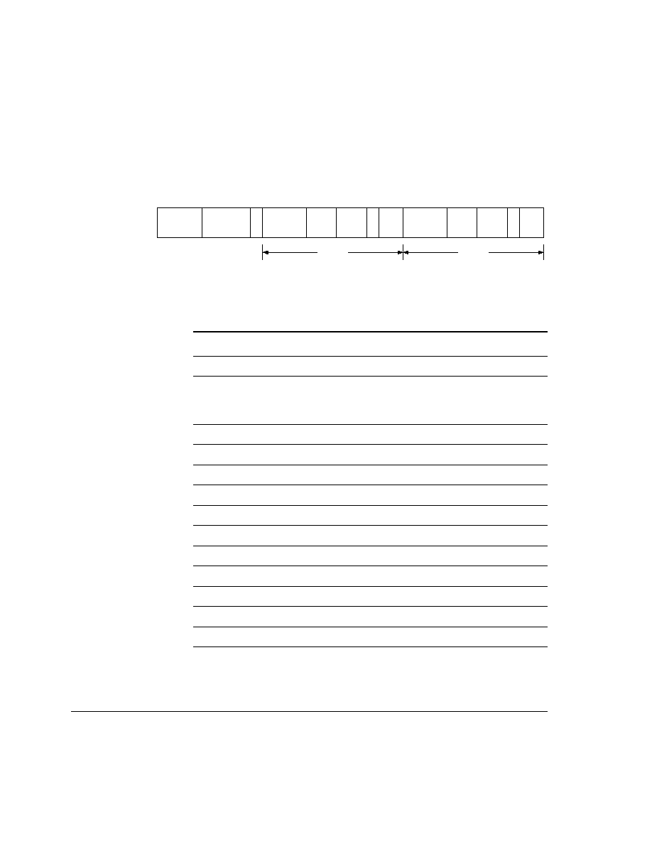
System Control Coprocessor
3-8
Copyright © 2001 ARM Limited. All rights reserved.
ARM DDI 0237A
Cache type register
Figure 3-4 shows the cache type register bit fields.
Figure 3-4 Cache type register
Table 3-5 describes the bit fields of the cache type register.
31
29 28
25 24 23
21 20 18 17 15 14 13 12 11
9 8
6 5
3 2 1 0
len
10
M
0
size
101
assoc
110
Reserved
000
S
1
ctype
0110
Reserved
000
len
10
M
0
size
101
assoc
110
Reserved
000
Isize
Dsize
Table 3-5 Encoding of the cache type register
Bits
Meaning
Value
Notes
[31:29] Reserved
000
-
[28:25]
Cache class
0110
Cache-clean-step operation
Cache-invalidate-step operation
Lock-down facilities
24
Harvard architecture
1
-
[23:21]
Reserved
000
-
[20:18]
Data cache sizes
101
16KB
[17:15]
Data cache associativity
110
64-way associative
14
Data cache parameters
0
Associativity and size are equal
[13:12]
Data cache line length
10
Eight words per line
[11:9]
Reserved
000
-
[8:6]
Instruction cache size
101
16KB
[5:3]
Instruction cache associativity
110
64-way set associative
2
Instruction cache parameters
0
Associativity and size are equal
[1:0]
Instruction cache line length
10
Eight words per line

System Control Coprocessor
ARM DDI 0237A
Copyright © 2001 ARM Limited. All rights reserved.
3-9
3.2.2
CP15 R1, control register 1
The read/write control register 1:
∑
enables fast interrupts
∑
selects the T bit after a load PC operation
∑
selects random or round-robin victim replacement
∑
selects high-address or low-address vector locations
∑
enables the ICache, DCache, and write buffer
∑
enables branch prediction
∑
enables ROM protection and MMU protection
∑
selects big-endian or little-endian operation
∑
enables fault checking of address alignment
∑
enables the MMU.
Use a read-modify-write sequence to access control register 1. For both reading and
writing, the CRm and
opcode_2
fields should be zero. Table 3-6 shows the instructions
for using control register 1.
All defined control bits are cleared on reset except:
∑
The V bit is cleared at reset if the HIVECSINIT signal is LOW, or set if the
HIVECSINIT signal is HIGH.
∑
The B bit is cleared at reset if the BIGENDINIT signal is LOW, or set if the
BIGENDINIT signal is HIGH.
Table 3-6 Control register 1 instructions
Operation
Data
Instruction
Read configuration
Configuration data
MRC p15, 0, Rd, c1, c0, 0
Write configuration
Configuration data
MCR p15, 0, Rd, c1, c0, 0

System Control Coprocessor
3-10
Copyright © 2001 ARM Limited. All rights reserved.
ARM DDI 0237A
Figure 3-5 shows the control register 1 bit fields.
Figure 3-5 Control register 1
Using a read-modify-write sequence when changing control register 1 provides the
greatest future compatibility. Table 3-7 describes the control register 1 bit fields.
M
A
W C
S B
R
I Z SBZ
L4 RR V
SBZ
FI
SBZ
Reset:
31
22 21 20
16 15 14 13 12 11 10 9 8 7 6 4 3 2 1 0
00 0000 0000
0
0 0000
0 0 0 0 0
0
SBO
0 0 0 111 1 0 0 0
Table 3-7 Encoding of control register 1
Bits
Name
Meaning
[31:22]
-
Reading returns an
UNPREDICTABLE
value. When written,
SHOULD BE ZERO
, or a value read from bits
[31:18] on the same processor.
21
FI
Fast interrupt bit. Disables HUM and reduces write buffer to half depth, or four doublewords.
Reset clears FI.
1 = write buffer is four slots, HUM disabled, streaming disabled, core is blocking
0 = write buffer is eight slots, HUM and streaming enabled, core is nonblocking
[20:16]
-
SHOULD BE ZERO
15
L4
When using an
LDR
instruction to load the PC, setting the L4 bit enables software written for ARM
architecture version 4 to be used. Reset clears L4.
1 = PC bit 0 is T bit
0 = T bit in CPSR is T bit
14
RR
ICache and DCache round-robin replacement bit. Reset clears RR.
1 = round-robin replacement enabled
0 = random replacement
13
V
Exception vector location bit. Reset clears V.
1 = vectors start at
0xFFFF 0000
0 = vectors start at
0x0000 0000
12
I
Instruction cache enable bit. Reset clears I.
1 = ICache enabled
0 = ICache disabled
11
Z
Branch prediction enable bit. Reset clears Z.
1 = branch prediction enabled
0 = branch prediction disabled
10
-
SHOULD BE ZERO

System Control Coprocessor
ARM DDI 0237A
Copyright © 2001 ARM Limited. All rights reserved.
3-11
Note
Be careful with the address mapping of the code sequence used to enable the MMU (see
Enabling the MMU on page 4-33).
See DCache and write buffer enable/disable on page 5-8 for restrictions, and for effects
of having caches enabled when the MMU is disabled.
9
R
ROM protection enable bit. Reset clears R.
1 = ROM protection enabled
0 = ROM protection disabled
8
S
System protection enable bit. Reset clears S.
1 = IMMU and DMMU protection enabled
0 = IMMU and DMMU protection disabled
7
B
Big-endian bit. Reset clears B.
1 = big-endian operation
0 = little-endian operation
[6:4]
-
Reading returns 111. When written,
SHOULD BE ONE
.
3
W
Write buffer enable bit. Reset sets W.
1 = write buffer enabled
0 = write buffer disabled
2
C
DCache enable bit. Reset clears C.
1 = DCache enabled
0 = DCache disabled
1
A
Address alignment fault checking enable bit. Reset clears A.
1 = fault checking of address alignment enabled
0 = fault checking of address alignment disabled
0
M
MMU enable bit. Reset clears M.
1 = IMMU and DMMU enabled
0 = IMMU and DMMU disabled
Table 3-7 Encoding of control register 1 (continued)
Bits
Name
Meaning

System Control Coprocessor
3-12
Copyright © 2001 ARM Limited. All rights reserved.
ARM DDI 0237A
3.2.3
CP15 R2, translation table base register
The Translation Table Base Register, TTBR, contains the Translation Table Base
(TTB) of the level 1 translation table.
When read, bits [31:14] return the pointer to the level 1 translation table, and bits [13:0]
return an
UNPREDICTABLE
value.
Writing to TTBR updates the pointer to the level 1 translation table in bits [31:14]. Bits
[13:0]
SHOULD BE ZERO
.
The CRm and
opcode_2
fields
SHOULD BE ZERO
when writing to TTBR.
Table 3-8 shows the instructions for using TTBR.
Figure 3-6 shows the TTBR bit fields.
Figure 3-6 Translation table base register
3.2.4
CP15 R3, domain access control register
The Domain Access Control Register, DACR, contains 16 discrete 2-bit domain access
control fields, each of which defines the access permissions for one of the 16 domains,
D15-D0.
Reading DACR returns the value of the domain access control bit fields. Writing to
DACR writes the value of the domain access control bitfields.
The CRm and
opcode_2
fields
SHOULD BE ZERO
when writing to DACR.
Table 3-8 Translation table base register instructions
Operation
Data
Instruction
Read TTB
TTB address
MRC p15, 0, Rd, c2, c0, 0
Write TTB
TTB address
MCR p15, 0, Rd, c2, c0, 0
31
14 13
0
SBZ
Translation table base

System Control Coprocessor
ARM DDI 0237A
Copyright © 2001 ARM Limited. All rights reserved.
3-13
Table 3-9 shows the instructions for using DACR.
Figure 3-7 shows the DACR bit fields.
Figure 3-7 Domain access control register
Table 3-10 describes the DACR bit fields.
Any write to DACR causes all unlocked TLB entries to be invalidated. If you change
the domain access control field corresponding to a locked TLB entry, you must
invalidate that entry in the TLB using the invalidate single entry operation and reload
it. Ideally, a program that locks entries in the TLB maps those locked entries to
unmodified DAC fields.
3.2.5
CP15 R4
Reading or writing CP15 R4 is
UNDEFINED
.
Table 3-9 Domain access control register instructions
Operation
Data
Instruction
Read domain access
Domain 15 to 0 access control
MRC p15, 0, Rd, c3, c0, 0
Write domain access
Domain 15 to 0 access control
MCR p15, 0, Rd, c3, c0, 0
31 30 29 28 27 26 25 24 23 22 21 20 19 18 17 16 15 14 13 12 11 10 9 8 7 6 5 4 3 2 1 0
D0
D1
D3
D2
D4
D5
D8
D7
D6
D9
D11 D10
D13 D12
D15 D14
Table 3-10 Encoding of the domain access control register
Bits
Meaning
D15-D0
Domain access control:
00 = no access; access generates domain fault.
01 = client access; access permissions are checked.
10 = reserved; behaves as no access domain.
11 = manager; access permissions are not checked.

System Control Coprocessor
3-14
Copyright © 2001 ARM Limited. All rights reserved.
ARM DDI 0237A
3.2.6
CP15 R5, fault status register
The Fault Status Register (FSR) contains the source of the last data fault. It indicates
the domain and type of access being attempted when an abort occurred.
Table 3-11 shows the instructions for using the FSR.
Figure 3-8 shows the FSR bit fields.
Figure 3-8 Fault status register
Table 3-12 describes the FSR bit fields.
Table 3-11 Fault status register instructions
Operation
Data
Instruction
Read data FSR
FSR data
MRC p15, 0, Rd, c5, c0, 0
Write data FSR
FSR data
MCR p15, 0, Rd, c5, c0, 0
Read instruction FSR
FSR instruction
MRC p15, 0, Rd, c5, c0, 1
Write instruction FSR
FSR instruction
MCR p15, 0, Rd, c5, c0, 1
Status
31
8 7
4 3
0
Domain
SBZ
Table 3-12 Encoding of the fault status register
Bits
Meaning
[31:8]
SHOULD BE ZERO
[7:4]
Domain selector that caused the abort. Specifies which of the 16 domains (D15-D0)
was being accessed when a fault occurred.
[3:0]
Type of fault generated (see Table 3-13 on page 3-15).

System Control Coprocessor
ARM DDI 0237A
Copyright © 2001 ARM Limited. All rights reserved.
3-15
Table 3-13 lists the types of fault in order of priority.
Reading FSR returns the value of the FSR.
Writing to FSR changes the FSR to the value of the data written. This is useful for a
debugger to restore the value of the FSR. The register must be written using a
read-modify-write sequence. Bits [31:8] should be zero.
The CRm field should be zero when reading or writing FSR.
The design includes both a data FSR and an instruction FSR. The data FSR is used to
check all Data Aborts and watchpoints. The data FSR maps the debug event to a
watchpoint. The instruction FSR is used to check all prefetch aborts and breakpoints.
The instruction FSR maps the debug event to a breakpoint.
Table 3-13 Priority of fault types
Priority
Source
Status
Domain
FAR
Highest
Alignment
0001
Invalid
Valid
TLB miss
0000
Invalid
Valid
External abort on translation 1st level
1100
Invalid
Valid
External abort on translation 2nd level
1110
Valid
Valid
Translation section
1110
Invalid
Valid
Translation page
0111
Valid
Valid
Domain section
1001
Valid
Valid
Domain page
1011
Valid
Valid
Permission section
1101
Valid
Valid
Permission page
1111
Valid
Valid
External abort
1010
Valid
Valid
Lowest
Debug event
0010
Valid
Valid

System Control Coprocessor
3-16
Copyright © 2001 ARM Limited. All rights reserved.
ARM DDI 0237A
3.2.7
CP15 R6, fault address register
The Fault Address Register (FAR) holds the VA of the access that was attempted when
a fault occurred.
Table 3-14 shows the instructions for using the FAR.
Reading FAR returns the value of either the data FAR or the instruction FAR as
specified by the
opcode_2
value.
Writing to FAR changes the FAR to the value of the data written. This is useful for a
debugger to restore the value of the FAR.
The CRm fields should be zero when reading or writing FAR.
Figure 3-9 shows the FAR bit field.
Figure 3-9 Fault address register
The data FAR contains the address of the memory access which caused the Data Abort.
The instruction FAR contains the address (PC + 8) of the memory access which caused
either a watchpoint or Data Abort.
Table 3-14 Fault address register instructions
Operation
Data
Instruction
Read data FAR
FAR data
MRC p15, 0, Rd, c6, c0, 0
Write data FAR
FAR data
MCR p15, 0, Rd, c6, c0, 0
Read instruction FAR
FAR data
MRC p15, 0, Rd, c6, c0, 1
Write instruction FAR
FAR data
MCR p15, 0, Rd, c6, c0, 1
Fault address
31
0

System Control Coprocessor
ARM DDI 0237A
Copyright © 2001 ARM Limited. All rights reserved.
3-17
3.2.8
CP15 R7, index and VA cache operations registers
The index and VA cache operations registers are write-only registers for managing the
ICache and DCache.
Table 3-15 shows the instructions for performing index and VA cache operations.
The
opcode_2
and CRm fields in the
MCR
instruction select the cache operation. Writing
opcode_2
or CRm values other than those shown in Table 3-15 is
UNPREDICTABLE
.
Reading the index and VA cache operations registers is
UNPREDICTABLE
.
Table 3-15 Cache operations register instructions
Function
Data
Instruction
Invalidate caches
SHOULD BE ZERO
MCR p15, 0, Rd, c7, c7, 0
Invalidate ICache
SHOULD BE ZERO
MCR p15, 0, Rd, c7, c5, 0
Invalidate ICache single entry using VA
Virtual address
MCR p15, 0, Rd, c7, c5, 1
Prefetch ICache line
Virtual address
MCR p15, 0, Rd, c7, c13, 1
Invalidate DCache
SHOULD BE ZERO
MCR p15, 0, Rd, c7, c6, 0
Invalidate DCache single entry using VA
Virtual address
MCR p15, 0, Rd, c7, c6, 1
Clean DCache single entry using VA
Virtual address
MCR p15, 0, Rd, c7, c10, 1
Clean and invalidate DCache single entry using VA
Virtual address
MCR p15, 0, Rd, c7, c14, 1
Clean DCache single entry using index
Index, segment format
MCR p15, 0, Rd, c7, c10, 2
Clean and invalidate DCache entry using index
Index, segment format
MCR p15, 0, Rd, c7, c14, 2
Empty write buffer
SHOULD BE ZERO
MCR p15, 0, Rd, c7, c10, 4
Wait for interrupt
SHOULD BE ZERO
MCR p15, 0, Rd, c7, c0, 4

System Control Coprocessor
3-18
Copyright © 2001 ARM Limited. All rights reserved.
ARM DDI 0237A
Table 3-16 describes the cache operations in more detail.
Note
Dirty data is data that has been modified in the cache but not yet copied back to main
memory.
Index cache operation register
The operations that act on a single cache line identify the line using the contents of
Rd
as the address, passed in the
MCR
instruction. Figure 3-10 shows the index cache
operation register.
Figure 3-10 Index cache operations register
Table 3-16 Cache operation descriptions
Function
Description
Invalidate cache
Invalidates all cache data, including any dirty data.
Use with caution.
Invalidate single entry using VA
Invalidates a single cache line, including any dirty data.
Use with caution.
Clean single DCache entry using
either index or VA
Writes the specified cache line to main memory if the line is marked valid and
dirty and is from a write-back memory region and marks the line as not dirty.
The valid bit is unchanged.
Clean and invalidate single DCache
entry using either index or VA
Writes the specified cache line to main memory if the line is marked valid and
dirty, and is from a write-back memory region.
The line is marked not valid.
Prefetch cache line
Performs an ICache lookup of the specified address.
If the cache misses, and the region is cachable, a linefill is performed.
31
26 25
9 8
5 4 3 2
0
Wd
SBZ
Sg
SBZ
Index

System Control Coprocessor
ARM DDI 0237A
Copyright © 2001 ARM Limited. All rights reserved.
3-19
Table 3-17 describes the bit fields of the index cache operation register.
The index tag format of Example 3-1 is for accessing a specific line in the cache.
Example 3-1 shows the command clean D single entry (using index).
Example 3-1 Clean D single entry (using index)
;code is specific to the ARM1022E macrocell with 16KB caches
MOV R0, #0:SHL:5
;select segment
seg_loop
MOV R1, #0:SHL:26
;select index
line_loop
ORR R2,R1,R0
MCR p15,0,R2,c7,c10,2
ADD R1,R1,#1:SHL:26
;increment index
CMP R1,#0
;check for index overflow
BNE line_loop
ADD R0,R0,#1:SHL:5
;increment segment
CMP R0,#1:SHL:8
;check for segment overflow
BNE seg_loop
Table 3-17 Encoding of the index cache operations register
Bits
Meaning
[31:26]
Index in segment being accessed
[25:9]
SHOULD BE ZERO
[8:5]
Segment being accessed
[4:3]
64-bit double word being accessed
[2:0]
SHOULD BE ZERO

System Control Coprocessor
3-20
Copyright © 2001 ARM Limited. All rights reserved.
ARM DDI 0237A
VA cache operations register
The VA cache operations register is useful for invalidating a particular address or range
of addresses in the caches. Figure 3-11 shows the bit fields of the VA cache operations
register.
Figure 3-11 VA cache operations register
Table 3-18 describes the bit fields of the VA cache operations register.
Note
ICache prefetch operations and DCache clean operations are performed
requested-word-first.
3.2.9
CP15 R8, TLB operations register
The TLB operations register is a write-only register for managing the instruction TLB
and the data TLB. Reading from the TLB operations register is
UNPREDICTABLE
.
SBZ
31
9 8
5 4 3 2
0
Wd
Sg
Virtual CAM tag
Table 3-18 Encoding of the VA cache operations register
Bits
Meaning
[31:9]
Virtual Content Addressable Memory (CAM) tag
[8:5]
Segment being accessed
[4:3]
64-bit double word being accessed
[2:0]
SHOULD BE ZERO

System Control Coprocessor
ARM DDI 0237A
Copyright © 2001 ARM Limited. All rights reserved.
3-21
Table 3-19 shows the instructions for performing TLB operations.
The
opcode_2
and CRm fields in the
MCR
instruction select the TLB operation. Writing
opcode_2
or CRm values other than those shown in Table 3-19 is
UNPREDICTABLE
.
Figure 3-12 shows the TLB operations register bit fields.
Figure 3-12 TLB operations register
Note
Invalidating the full TLB invalidates all the unlocked entries in the TLB. Invalidating
TLB single entry functions invalidates any TLB entry corresponding to the VA given in
Rd
, regardless of its locked state (see CP15 R10, TLB lockdown register on page 3-23).
Table 3-19 TLB operations register instructions
Operation
Data
Instruction
Invalidate instruction and data TLBs
SHOULD BE ZERO
MCR p15, 0, Rd, c8, c7, 0
Invalidate instruction TLB
SHOULD BE ZERO
MCR p15, 0, Rd, c8, c5, 0
Invalidate instructionTLB single entry (using VA)
Virtual address
MCR p15, 0, Rd, c8, c5, 1
Invalidate data TLB
SHOULD BE ZERO
MCR p15, 0, Rd, c8, c6, 0
Invalidate data TLB single entry (using VA)
Virtual address
MCR p15, 0, Rd, c8, c6, 1
SBZ
31
5 4
0
Virtual CAM tag

System Control Coprocessor
3-22
Copyright © 2001 ARM Limited. All rights reserved.
ARM DDI 0237A
3.2.10
CP15 R9, cache lockdown register
The cache lockdown register enables software to:
∑
control which line ICache or DCache line is loaded for a linefill by changing the
base value or the victim counter value respectively
∑
prevent ICache or DCache lines from being replaced during a linefill, locking
them into the cache.
Table 3-20 shows the instructions for using the cache lockdown register.
Reading the cache lockdown register returns the value of the cache lockdown register,
which is the base pointer for all cache segments. Reset clears the cache lockdown
register.
Note
Only bits [31:26] are returned. Bits [25:0] are zero.
Figure 3-13 shows the bit fields of the cache lockdown register
Figure 3-13 Cache lockdown register
Writing to the cache lockdown register updates the base pointer and the current victim
counter value for all cache segments. Bits [25:0]
SHOULD BE ZERO
. The next linefill uses
the victim counter value, then increments the victim counter. The victim counter
continues incrementing on linefills and wraps around to the base pointer. For example,
setting the base pointer to
0x3
prevents the victim counter from selecting entries
0x0
to
0x2
, locking them into the cache.
Table 3-20 Cache lockdown register instructions
Operation
Data
Instruction
Read DCache lockdown base
Base
MRC p15, 0, Rd, c9, c0, 0
Write DCache victim and lockdown base
Victim = base
MCR p15, 0, Rd, c9, c0, 0
Read ICache lockdown base
Base
MRC p15, 0, Rd, c9, c0, 1
Write ICache victim and lockdown base
Victim = base
MCR p15, 0, Rd, c9, c0, 1
31
26
UNP/SBZ
Base value
25
0

System Control Coprocessor
ARM DDI 0237A
Copyright © 2001 ARM Limited. All rights reserved.
3-23
The victim counter specifies the cache line to be used as the victim for the next linefill.
The counter is incremented using either a random or round-robin replacement policy,
determined by the state of the RR bit in control register 1, CP15 R1. The victim counter
generates values from base to base + 63. This locks lines with index values from 0 to
base ≠ 1, with an upper limit of 63 locked entries in the DCache. If base = 0 there are
no locked lines.
Example 3-2 shows how to load a single entry into line 0 and lock it down.
Example 3-2 Updating the base pointer and current victim pointer
MCR to CP15 r9, Victim=Base=0x0
MCR to cause an I prefetch, LDR/LDM, depending on whether it is ICache or
DCache. Assuming the appropriate cache misses, a linefill occurs to line 0.
MCR to CP15 r9, Victim=Base=0x1
Further linefills now occur into lines 1 to 63.
3.2.11
CP15 R10, TLB lockdown register
There is a TLB lockdown register for each TLB. Reading the TLB lockdown register
returns the value of the TLB lockdown counter base register, the current victim counter
value, and the preserve bit. The TLB lockdown register is cleared at reset.
Writing to the TLB lockdown register updates the TLB lockdown counter base register,
the current victim counter value, and the state of the preserve bit. Bits [19:1]
SHOULD BE
ZERO
. Table 3-21 shows the instructions for using the TLB lockdown register.
Table 3-21 TLB lockdown register instructions
Operation
Data
Instruction
Read data TLB lockdown
TLB lockdown
MRC p15, 0, Rd, c10, c0, 0
Write data TLB lockdown
TLB lockdown
MCR p15, 0, Rd, c10, c0, 0
Read instruction TLB lockdown
TLB lockdown
MRC p15, 0, Rd, c10, c0, 1
Write instruction TLB lockdown
TLB lockdown
MCR p15, 0, Rd, c10, c0, 1

System Control Coprocessor
3-24
Copyright © 2001 ARM Limited. All rights reserved.
ARM DDI 0237A
Figure 3-14 shows the bit fields of the TLB lockdown register.
Figure 3-14 TLB lockdown register
The entries in the TLBs are replaced using a round-robin replacement policy. This is
implemented using a victim counter that counts up continuously from entry 0 at the base
value to entry 63, wrapping back from 63 to the base value each time.
There are two mechanisms to ensure that entries are not removed from the TLB:
∑
Locking an entry down prevents it from being selected for overwriting during a
table walk. This is achieved by programming the base value to which the victim
counter reloads. For example, if the bottom three entries (0 to 2) are to be locked
down, the base counter must be programmed to 3.
∑
An entry can also be preserved during an invalidate all instruction. This is done
by ensuring the P bit is set when the entry is loaded into the TLB.
Example 3-3 shows how to load a single entry into location 0, make it immune to
invalidate all, and lock it down.
Example 3-3 Ensuring an entry is not removed from the TLB
MCR to CP15 r10, Base Value = 0, Current Victim = 0, Preserve = `1'
MCR to cause prefetch, assuming a miss occurs in the TLB then entry 0 is loaded.
MCR to CP15 r10, Base Value = 1, Current Victim = 1, Preserve = `0'
3.2.12
CP15 R11
Reading or writing R11 takes the
UNDEFINED
instruction trap.
3.2.13
CP15 R12
Reading or writing R12 takes the
UNDEFINED
instruction trap.
P
31
26 25
20 19
1 0
SBZ
Base value
Current victim

System Control Coprocessor
ARM DDI 0237A
Copyright © 2001 ARM Limited. All rights reserved.
3-25
3.2.14
CP15 R13, process ID and context ID registers
The process ID and context ID registers are read/write registers. Reset clears the process
ID register.
Table 3-22 shows the instructions for using the process ID and context ID registers.
Reading the process ID register returns the value of the process ID.
Writing to the process ID register updates the process ID. Bits [24:0] should be zero.
Figure 3-15 shows the bit fields of the process ID register.
Figure 3-15 Process ID register
The context ID register is a holding register for storing the current context of the
program. Reading the context ID register returns the context ID. Writing to the context
ID register updates the context ID.
Figure 3-16 shows the bit fields of the context ID register.
Figure 3-16 Context ID register
Table 3-22 Process ID and context ID register instructions
Operation
Instruction
Read process ID
MRC p15, 0, Rd, c13, c0, 0
Write process ID
MCR p15, 0, Rd, c13, c0, 0
Read context ID
MRC p15, 0, Rd, c13, c0, 1
Write context ID
MCR p15, 0, Rd, c13, c0, 1
31
25 24
0
SBZ
Process ID
Context ID
31
0

System Control Coprocessor
3-26
Copyright © 2001 ARM Limited. All rights reserved.
ARM DDI 0237A
Using the process ID
Addresses issued by the integer unit in the range 0 to 32MB are translated by the process
ID. Address A becomes A + (process ID
◊
32MB). This translated address is used by
both the caches and MMU. Addresses above 32MB are not translated. This is shown in
Figure 3-17. The process ID is a seven-bit field, enabling 128
◊
32MB processes to be
mapped.
Note
If the process ID is zero, as it is on reset, then a flat mapping exists between the integer
unit, the caches, and the MMU.
Figure 3-17 Address mapping using CP15 R13
A fast context switch is performed by writing to the context ID register. The contents of
the caches and TLBs do not have to be invalidated after a fast context switch because
they still hold valid address tags. From two to five instructions can be fetched with the
old process ID after the
MCR
that writes to the process ID:
4GB
4GB
Process ID No 128
0
32MB
64MB
Address issued by ARM10E
Address input to caches and MMU
Process ID No 1
Process ID No 0
Process ID No 2
32MB
0

System Control Coprocessor
ARM DDI 0237A
Copyright © 2001 ARM Limited. All rights reserved.
3-27
Example 3-4 Changing the process ID and performing a fast context switch
{procID = 0}
MOV r0, #1; Fetched with procID = 0
MCR p15,0,r0,c13,c0,0
; Fetched with procID = 0
A0
(any instruction)
; Fetched with procID = 0
A1
(any instruction)
; Fetched with procID = 0
A2
(any instruction)
; Fetched with procID = 0/1
A3
(any instruction)
; Fetched with procID = 0/1
A4
(any instruction)
; Fetched with procID = 0/1
A5
(any instruction)
; Fetched with procID = 1
3.2.15
CP15 R14
Reading or writing CP15 R14 is
UNDEFINED
.
3.2.16
CP15 R15
CP15 R15 is used for test purposes. Reading or writing CP15 R15 in normal operation
is
UNPREDICTABLE
.
R15 functions are described in:
∑
PLL configuration register on page 3-28
∑
Power manager status register on page 3-29
∑
Power manager receive data register on page 3-30
∑
Power manager transmit data register on page 3-31
∑
Transmission protocol on page 3-32
∑
Control register 2 on page 3-33.

System Control Coprocessor
3-28
Copyright © 2001 ARM Limited. All rights reserved.
ARM DDI 0237A
PLL configuration register
The PLL configuration register is for reprogramming the core clock frequency or AHB
bus frequency. The register has a defined reset value as shown in Figure 3-18. Refer to
Chapter 14 Clock Generator for more details.
Table 3-23 shows the instructions for using the PLL configuration register.
Figure 3-18 shows the bit fields of the PLL configuration register.
Figure 3-18 PLL configuration register
Table 3-24 describes the bit fields of the PLL configuration register.
Table 3-23 PLL configuration register instructions
Operation
Instruction
Read status
MRC p15, 0, Rd, c15, c12, 0
Write configuration
MCR p15, 0, Rd, c15, c12, 0
Reset:
HDIV[3:0]
31
24
23 22
17
16
15
14 13 12 11
0
SBZ
POWERDN BYPASS[1:0]
PCONFIGOUT[1:0]
SBZ
3
MDIV[7:0]
4
25
PCONFIGIN[5:0]
00
00 0000
0000 0000
1111
1
11
Table 3-24 Encoding of the PLL configuration register
Bits
Meaning
[31:25]
SHOULD BE ZERO
[24:23]
Bit 24 is for a partner-defined PLL function. Bit 23 is for a lock-detect signal.
[22:17]
Partner-specific PLL functions
16
POWERDN PLL draws only minimum leakage current due to VCO being
clamped. Lock is lost.
[15:14]
BYPASS [1:0] Controls the selects for the GCLK, HCLK, and VCO
multiplexors. See Chapter 14 Clock Generator.
[13:12]
SHOULD BE ZERO
[11:4]
PLL feedback divider (MCLK) MDIV[7:0]
[3:0]
AHB clock divider (HCLK) HDIV[3:0]

System Control Coprocessor
ARM DDI 0237A
Copyright © 2001 ARM Limited. All rights reserved.
3-29
Power manager status register
The Power Manager Status Register, PMSR, contains the version number of the power
manager. It also indicates when the receive channel is available to check the last state
of the system, and when the transmit channel is available to send new data.
Table 3-25 shows the instructions for using PMSR.
Figure 3-19 shows the PMSR bit fields.
Figure 3-19 Power manager status register
Table 3-26 describes the PMSR bit fields.
Table 3-25 Power manager status instructions
Operation
Instruction
Read status
MRC p15, 0, Rd, c15, c14, 0
Check receive channel
MRC p15, 0, Rd, c15, c14, 1
Write transmit channel
MCR p15, 0, Rn, c15, c14, 1
R
31
28 27
2 1 0
W
SBZ
Version
Table 3-26 Encoding of the power manager status register
Bits
Meaning
[31:28]
Version =
0x000
1
[27:2]
SHOULD BE ZERO
1
Denotes transmit channel is ready:
1 = Idle
0 = Busy
0
Denotes receive channel is full:
1 = Full
0 = Empty

System Control Coprocessor
3-30
Copyright © 2001 ARM Limited. All rights reserved.
ARM DDI 0237A
Power manager receive data register
When the R flag in power manager status register is set, valid data can be read from the
Power Manager Receive Data Register, PMRDR. An acknowledgement is sent to the
power manager to indicate data acceptance. When the R flag is clear, reading PMRDR
is
UNPREDICTABLE
. Writing to PMRDR is
UNPREDICTABLE
. Figure 3-20 shows the PMRDR
bit fields.
Figure 3-20 Power manager receive data register
Table 3-27 describes the PMRDR bit fields.
SBZ
31
State
E
SBZ
30
8
3
0
7
4
Table 3-27 Encoding of the power manager receive data register
Bits
Meaning
31
Emulation flag. When exiting a reset sequence, E reflects the last programmed
state of the system.
1 = power manager issued a command in emulation mode
0 = power manager issued a command in normal mode
[30:8]
Reserved. Reads as zero.
[7:4]
System power state. When exiting a reset sequence, this field reflects the last
programmed state of the system.
1111 = TURBO
1110 = NORMAL
110x = SLOW
100x = IDLE
01xx = NAP
0011 = SLEEP
0010 = COMA
0001 = HIBERNATE
0000 = OFF
[3:0]
Reserved. Reads as zero.

System Control Coprocessor
ARM DDI 0237A
Copyright © 2001 ARM Limited. All rights reserved.
3-31
Power manager transmit data register
When the W flag in power manager status register is set, new data can be written to the
Power Manager Transmit Data Register, PMTDR. An acknowledgement following the
write is sent to the power manager to indicate that new data is available. Writing to
PMTDR clears W. Writing to PMTDR when W is clear is
UNPREDICTABLE
. Reading
PMTDR is
UNPREDICTABLE
. Figure 3-21 shows the PMTDR bit fields.
Figure 3-21 Power manager transmit data register
Table 3-28 describes the PMTDR bit fields.
SBZ
31
State
E
SBZ
30
8
3
0
7
4
Table 3-28 Encoding of the power manager transmit data register
Bits Name
Meaning
31
E
1 = power manager issued a command in emulation mode
0 = power manager issued a command in normal mode
[30:8]
-
SHOULD BE ZERO
[7:4]
State
System power state. When exiting a reset sequence, this value reflects the last
programmed state of the system.
1111 = TURBO
1110 = NORMAL
110x = SLOW
100x = IDLE
01xx = NAP
0011 = SLEEP
0010 = COMA
0001 = HIBERNATE
0000 = OFF
[3:0]
-
SHOULD BE ZERO

System Control Coprocessor
3-32
Copyright © 2001 ARM Limited. All rights reserved.
ARM DDI 0237A
Transmission protocol
When issuing commands to the power manager, a specific protocol must be followed:
1.
By reading the W and R flags, software checks to see that both transmit data and
receive data data bit fields are empty.
2.
When transmitting, software must write a command to the transmit data register.
This clears the W flag. Hardware then performs a handshake with the power
manager, waiting for acceptance of the command using a double-ended
handshake.
3.
When the handshake for the transmit data is done, hardware sets the W flag.
When receiving data, software must wait until the R flag is set. When set, new data is
valid in the receive data register.
Data Transmit Code
To transmit data to the power manager, software must always perform the code
sequence shown below. The command is sent using register ARM register R1, while
ARM register R0 reflects the status register contents:
tx_command:
MRC CP15, 0, R0, C15, C14, 0
; check for outstanding commands
TST R0, #W_flag
; `W' flag clear indicates active command
BNE tx_command
; if command active, loop again
MCR CP15, 0, R1, C15, C14, 1
; write new command to controller
Note
The W flag is polled until it is one. When W is set, the command can be sent to the
power manager.
Data Receive Code
To wait until data has been received in the receive data register, software must always
perform the code sequence shown below. The command is received into register ARM
register R1, while ARM register R0 reflects the status register contents:
rx_status
:
MRC CP15, 0, R0, C15, C14, 0
; check for incoming data
TST R0, #R_flag
; `R' flag clear indicates no data
BNE rx_status
; if no data, loop again
MRC CP15, 0, R0, C15, C14, 1
; read in `previous-state'

System Control Coprocessor
ARM DDI 0237A
Copyright © 2001 ARM Limited. All rights reserved.
3-33
Note
The R flag is polled until it is cleared. When R is cleared, the command can be read.
Control register 2
The read/write control register 2 is primarily useful when in debug mode. When not in
debug mode, it is also useful to define the behavior of accesses when the caches are on
and the DMMU is off.
Table 3-29 shows the instructions for using control register 2.
Figure 3-22 shows control register 2.
Figure 3-22 Control register 2
Table 3-30 describes the bit fields of control register 2.
Table 3-29 Control register 2 instructions
Operation
Instruction
Read status
MRC p15, 0, Rd, c15, c11, 0
Write
MCR p15, 0, Rd, c15, c11, 0
DB
4 3 2 1 0
DC
ST IC IB
SBZ
31
5
0 0 0 0
0
000 0000 0000 0000 0000 0000 0000
Reset:
Table 3-30 Encoding of control register 2
Bits
Meaning
[31:5]
SHOULD BE ZERO
4
ST, CP15 soft TLB enable bit. Reset clears ST.
1 = soft TLB enabled
0 = soft TLB disabled
3
IC, CP15 instruction cachable bit; used only in debug mode with the ICache on.
Reset clears IC.
1 = instructions cachable
0 = instructions not cachable

System Control Coprocessor
3-34
Copyright © 2001 ARM Limited. All rights reserved.
ARM DDI 0237A
2
IB, CP15 instruction bufferable bit. Used only in debug mode with the ICache on.
Included for compatability with the B bit in the MMU descriptors. Reset clears IB.
1 = instructions bufferable
0 = instructions not bufferable
1
DC, CP15 data cachable bit. Used in debug mode or when the DMMU is off and the
DCache is on. Reset clears DC.
1 = data cachable
0 = data not cachable
0
DB, CP15 data bufferable bit; used in debug mode or when the DMMU is off and
the DCache is on. Reset clears DB.
1 = data bufferable
0 = data not bufferable
Table 3-30 Encoding of control register 2
Bits
Meaning

ARM DDI 0237A
Copyright © 2001 ARM Limited. All rights reserved.
4-1
Chapter 4
Memory Management Units
This chapter describes the ARMv5 Memory Management Units (MMUs). It contains
the following sections:
∑
About the MMUs on page 4-2
∑
MMU software-accessible registers on page 4-3
∑
Address translation on page 4-5
∑
MMU memory access control on page 4-21
∑
MMU cachable and bufferable information on page 4-23
∑
MMU and write buffer on page 4-24
∑
MMU aborts on page 4-25
∑
MMU fault checking sequence on page 4-26
∑
CPU aborts on MMU faults on page 4-29
∑
Fault priority on page 4-30
∑
External aborts on page 4-31
∑
Interaction of the MMU, caches, and write buffer on page 4-33
∑
Soft page table support on page 4-34.

Memory Management Units
4-2
Copyright © 2001 ARM Limited. All rights reserved.
ARM DDI 0237A
4.1
About the MMUs
The MMUs control external memory accesses and translate Virtual Addresses (VAs) to
Physical Addresses (PAs).
The Instruction MMU (IMMU) and Data MMU (DMMU) provide address translation
and access permission checks for the instruction and data ports of the integer unit. They
control the descriptor fetch hardware that accesses page table descriptors in main
memory. To support sections and pages, there are two levels of page tables. The finished
VA-to-PA translations are put into separate instruction-side and data-side Translation
Lookaside Buffers (TLBs).
MMU features include:
∑
standard MMU mapping sizes, domains, and access protection
∑
1KB, 4KB, 64KB, and 1MB mapping sizes
∑
access permissions for 1MB sections
∑
separate access permissions for one-quarter page subpages of 64KB large pages
and 4KB small pages
∑
16 domains
∑
separate 64-entry instruction and data TLBs
∑
independent lockdown of instruction and data TLBs
∑
hardware page table descriptor fetches
∑
round-robin replacement algorithm
∑
support for soft page tables.

Memory Management Units
ARM DDI 0237A
Copyright © 2001 ARM Limited. All rights reserved.
4-3
4.2
MMU software-accessible registers
The CP15 registers shown in Table 4-1, along with the page table descriptors stored in
memory, control MMU operation.
Table 4-1 CP15 register MMU functions
CP15 register
Bits
Register description
R1
Control register 1
M
A
S
R
Bit 0, MMU enable bit:
1 = IMMU and DMMU enabled
0 = IMMU and DMMU disabled
Bit 1, address alignment fault checking enable bit:
1 = fault checking of address alignment enabled
0 = fault checking of address alignment disabled
Bit 8, system protection enable bit:
1 = IMMU and DMMU protection enabled
0 = IMMU and DMMU protection disabled
Bit 9, ROM protection enable bit:
1 = ROM protection enabled
0 = ROM protection disabled
R2
Translation table base register
[31:14]
Holds PA of base of translation table in main memory. Base must reside on
a 16KB boundary and is common to both IMMU and DMMU.
R3
Domain access control register
[31:0]
Has 16 2-bit fields. Each field defines the access control attributes for one
of 16 domains (D15-D0). See Table 4-5 on page 4-21
R5
Fault status register
[31:8]
[7:4]
[3:0]
Indicates domain number and cause of Data Abort.
SHOULD BE ZERO
Indicate domain (D15-D0) in which fault occurred.
Indicate type of access attempted. See Table 4-8 on page 4-30.
R6
Fault address register
[31: 0]
Holds VA associated with access that caused Abort. See CP15 R6, fault
address register on page 3-16 for FAR access instructions. See Table 4-8
on page 4-30 for details of the address stored for each type of fault.

Memory Management Units
4-4
Copyright © 2001 ARM Limited. All rights reserved.
ARM DDI 0237A
Note
All the CP15 MMU registers, except CP15 R8, contain state and can be read using
MRC
instructions and written to using
MCR
instructions. CP15 R5 and CP15 R6 are also
written by the MMU. Reading CP15 R8 is
UNPREDICTABLE
.
R8
TLB operations register
[31:5]
Writing to R8 causes the MMU to perform TLB maintenance operations,
invalidating one or all unpreserved TLB entries.
R10
TLB lockdown register
[31:20], 0
Allows specific page table entries to be locked into a TLB and the TLB
victim counter to be read/written.
Locking entries in a TLB guarantees that accesses to the locked page or
section can proceed without incurring the time penalty of a TLB miss. This
enables the execution latency for time-critical pieces of code such as IRQ
handlers to be minimized.
R15
Control register 2
[4]
Allows the MMU to be configured for soft TLB support.
Table 4-1 CP15 register MMU functions (continued)
CP15 register
Bits
Register description

Memory Management Units
ARM DDI 0237A
Copyright © 2001 ARM Limited. All rights reserved.
4-5
4.3
Address translation
The address translation process begins when the integer unit requests access to an
address that has no VA-to-PA translation in the TLB, causing a TLB miss. The MMU
then fetches a page table descriptor.
4.3.1
TLBs
Each TLB caches 64 translated entries. If, during a memory access, the TLB contains a
translated entry for the VA, the MMU reads the protection data to determine if the
access is permitted:
∑
If the access is permitted, and off-chip access is required, the MMU produces the
PA.
∑
If the access is permitted, and off-chip access is not required, the cache services
the access.
∑
If the access is not permitted, the MMU signals the CPU to abort.
If a TLB miss occurs, the page table descriptor fetch hardware retrieves the translation
information from a translation table in main memory. The retrieved information is
written into the TLB, possibly overwriting an existing value.
The entry to be written is usually chosen by cycling sequentially through the TLB
locations. To enable use of TLB locking features, the location to be written can be
specified using the TLB lockdown register, CP15 R10.
When the MMU is turned off, as happens at reset, no address mapping occurs, and all
regions are marked as noncachable and nonbufferable.

Memory Management Units
4-6
Copyright © 2001 ARM Limited. All rights reserved.
ARM DDI 0237A
4.3.2
Page table descriptor fetches
A page table descriptor fetch occurs whenever there is a TLB miss. The descriptor fetch
begins with the formation of a level 1 descriptor.
Note
If the DMMU is performing an external memory operation for the load/store unit, the
write buffer is emptied before the descriptor fetch. This guarantees that memory
remains coherent. The DMMU then performs the operation as noncachable and
nonbufferable.
IMMU activity does not cause the write buffer to be emptied.
4.3.3
Translation routes for sections and pages
The MMU translates VAs from the integer unit to PAs for an external memory access.
The two types of memory blocks, sections and pages, require a specific translation
process to occur.
Figure 4-1 on page 4-7 shows the translation process. A section requires only a level 1
descriptor fetch. A page requires both a level 1 and level 2 descriptor fetch.

Memory Management Units
ARM DDI 0237A
Copyright © 2001 ARM Limited. All rights reserved.
4-7
Figure 4-1 Translating pages and section addresses
Translation
table base
Indexed by
VA[31:20]
Base address
from L1D[31:10]
Level 1
page table
descriptors
16KB
31
0
00
Base address
from L2D[31:16]
Base address
from L2D[31:12]
01
10
11
Base address
from L1D[31:20]
1MB section
Indexed by
VA[19:0]
4KB small page
1KB subpage
1KB subpage
1KB subpage
1KB subpage
Indexed by
VA[11:0]
64KB large page
Indexed by
VA[15:0]
16KB subpage
16KB subpage
16KB subpage
16KB subpage
Indexed by
VA[19:12]
Level 2 coarse
page table
descriptors
1KB
31
0
Invalid 00
Invalid 11
10
01
Base address
from L2D[31:16]
Base address
from L2D[31:12]
Base address
from L2D[31:10]
Base address
from L1D[31:12]
Indexed by
VA[19:10]
Level 2 fine
page table
descriptors
4KB
31
0
Invalid 00
11
10
01
1KB subpage
1KB subpage
1KB subpage
1KB subpage
4KB small page
Indexed by
VA[11:0]
1KB tiny page
Indexed by
VA[9:0]
16KB subpage
16KB subpage
16KB subpage
16KB subpage
64KB large page
Indexed by
VA[15:0]
Level 1
Level 2
Pages/sections
7
0
7
0
7
0
7
0
7
0
7
0

Memory Management Units
4-8
Copyright © 2001 ARM Limited. All rights reserved.
ARM DDI 0237A
4.3.4
Level 1 descriptor address
Figure 4-2 shows how the MMU uses the translation table base field in CP15 R2 and
the VA from the integer unit to create the level 1 descriptor address.
Figure 4-2 Translating a level 1 descriptor address
4.3.5
Level 1 page table descriptors
The level 1 descriptor indicates whether the access is:
∑
a translation fault
∑
an access to a level 2 coarse page table
∑
an access to a 1MB section of external memory
∑
an access to a level 2 fine page table.
Bits [1:0] of the level 1 descriptor determine the type of access. Figure 4-3 on page 4-9
shows the level 1 descriptor formats for the three access types.
SBZ
0
13
14
31
Translation table base
Translation
table base
Not used
19
0
Level 1 table index
20
31
Virtual
address
13
14
Level 1 table index
0
1
2
0
0
Translation table base
31
Level 1
descriptor
address

Memory Management Units
ARM DDI 0237A
Copyright © 2001 ARM Limited. All rights reserved.
4-9
Figure 4-3 Level 1 descriptor formats
Using the level 1 descriptor address, the MMU makes a request to external memory.
This returns the level 1 descriptor. Bits [1:0] of the level 1 descriptor indicate the access
type as Table 4-2 shows.
Level 1 translation fault
If bits [1:0] of the level 1 descriptor are 00, a translation fault is generated. This causes
either a Prefetch Abort or Data Abort in the integer unit. A Prefetch Abort occurs in the
IMMU. A Data Abort occurs in the DMMU.
Level 1 coarse page table address
If bits [1:0] of the level 1 descriptor are 01, then a descriptor fetch from a coarse page
table is required. Figure 4-6 on page 4-12 shows how the MMU generates a coarse page
table address.
31
20 19
12 11 10
9
8
5 4
1 0
0
0
1
0
1 SBZ
Domain selector
SBZ
Level 2 coarse page table base address
0
1
1 C B
AP
Section base address
SBZ
1
1
1
Level 2 fine page table base address
3 2
SBZ
Domain selector
Domain selector
SBZ
SBZ
Ignore
Translation fault
Coarse page table
1MB section
Fine page table
Table 4-2 Access types from level 1 descriptor
Bits [1:0]
Access type
00
Translation fault
01
Coarse page table base address
10
Section base address
11
Fine page table base address

Memory Management Units
4-10
Copyright © 2001 ARM Limited. All rights reserved.
ARM DDI 0237A
Level 1 section base address
If bits [1:0] of the level 1 descriptor are 10, a request to access a 1MB memory section
is requested. Figure 4-4 shows the translation process for a 1MB section.
Figure 4-4 Translating a section address
Following the level 1 descriptor translation, the the MMU uses the PA to transfer the
requested data between external memory and the integer unit. This is done only after
the domain and access permission checks are performed on the level 1 descriptor for the
section. These checks are described in MMU memory access control on page 4-21.
Level 1 fine page table base address
If bits [1:0] of the level 1 descriptor are 11, then a descriptor fetch from a fine page table
is required. This is shown in Figure 4-9 on page 4-16.
10 9
SBZ
0
13
14
31
Translation table base
Translation
table base
13
14
Level 1 table index
0
1
2
0
0
Translation table base
31
Level 1
descriptor
address
Section index
19
0
Level 1 table index
20
31
Virtual
address
Domain
selector
19
0
Section base address
20
31
Level 1
descriptor
1211
AP
S
B
Z
8
5 4 3 2 1
0
1
C B
1
Level 1 fetch
Section index
19
0
Section base address
20
31
Physical
address
SBZ

Memory Management Units
ARM DDI 0237A
Copyright © 2001 ARM Limited. All rights reserved.
4-11
4.3.6
Level 2 descriptor
If the level 1 descriptor points to a page table, the MMU determines the page table type,
coarse or fine, and fetches a level 2 descriptor. The level 2 descriptor indicates whether
the access is:
∑
a translation fault
∑
an access from a coarse page table to a large page with 64K 8-bit entries
∑
an access from a coarse page table to a small page with 4K 8-bit entries
∑
an access from a fine page table to a large page, a small page, or a tiny page with
1K 8-bit entries.
Figure 4-5 shows the level 2 descriptor formats for selecting page types.
Figure 4-5 Level 2 descriptor formats
Bits [1:0] of the level 2 descriptor indicate the page type. A large page can be divided
four 16KB subpages with different access permissions. Bits [15:14] of the VA page
index select the subpages of a large page.
A small page can be divided into four 1KB subpages with different access permissions.
Bits[11:10] of the VA page index select the subpages of a small page.
Level 2 coarse page table descriptor fetch
When the level 1 descriptor bits [1:0] indicate a descriptor fetch from a coarse page
table is required, the MMU requests the address of the level 2 coarse page table from
external memory. Figure 4-6 on page 4-12 shows how the address is generated.
0
1
0
B
AP3
Large page base address
0
1
C B
Small page base address
1
1
AP
Tiny page base address
SBZ
Ignore
Translation fault
64KB large page
4KB small page
1KB tiny page
0
31
16 15
12 11 10 9 8 7 6 5 4 3 2 1 0
SBZ
AP2 AP1 AP0 C
AP3 AP2 AP1 AP0
C B

Memory Management Units
4-12
Copyright © 2001 ARM Limited. All rights reserved.
ARM DDI 0237A
Figure 4-6 Translating a coarse page table address
When the coarse page table address is generated, a request is made to external memory
for the level 2 coarse page table descriptor. Bits [1:0] of the level 2 coarse page table
descriptor indicate the access type as shown in Table 4-3.
Virtual
address
10 9
SBZ
0
13
14
31
Translation table base
Translation table base
register, CP15 R2
13
14
Level 1 table index
0
1
2
0
0
Translation table base
31
Level 1
descriptor
address
Level 2
table index
19
0
Level 1 table index
20
31
Domain
selector
0
Page table base address
31
Level 1
descriptor
Not used
S
B
Z
8
5 4
1
1
0
1
Level 1 fetch
S
B
Z
3 2
12 11
0
Page table base address
31
Level 2
table index
1
0
1
2
9
10
Level 2
descriptor
address
Table 4-3 Access types from level 2 descriptor
Bits[1:0]
Access type
00
Translation fault
01
64KB large page base address
10
4KB small page base address
11
Translation fault

Memory Management Units
ARM DDI 0237A
Copyright © 2001 ARM Limited. All rights reserved.
4-13
Level 2 coarse translation fault
If bits [1:0] of the level 2 coarse page table descriptor are 00 or 11, then a translation
fault is generated. This generates an abort to the integer unit, either a Prefetch Abort for
the instruction side or a Data Abort for the data side.
Level 2 coarse large page base address
If bits [1:0] of the level 2 coarse page table descriptor are 01, then a descriptor fetch
from a coarse large page table is required. Figure 4-7 on page 4-14 shows the translation
process for a 64KB large page or a 16KB subpage of a large page.

Memory Management Units
4-14
Copyright © 2001 ARM Limited. All rights reserved.
ARM DDI 0237A
Figure 4-7 Translating a large page or subpage address from a coarse page table
The 64KB large page is generated by setting all of the AP bit pairs to the same values,
AP3 = AP2 = AP1 = AP0. If any one of the pairs is different, then the 64KB large page
is converted into four 16KB subpages.
Level 1
descriptor
address
0
1
2
Virtual
address
Translation table base
register, CP15 R2
Level 2
table index
Level 1 table index
20
31
Level 1
descriptor
Page index
Level 1
fetch
15
Level 2
descriptor
address
16
0
Page table base address
31
Level 2
table index
0 0
1
10
0
31
1
2
9
10
Level 2
descriptor
13
14
31
Level 1 table index
0
0
Translation table base
SBZ
0
13
14
31
Translation table base
Level 2
fetch
1211
8 7 6 5 4 3
Page base address
SBZ
A
P
3
A
P
2
A
P
1
A
P
0
C B 0
11
19
12
0
Physical
address
0
Page base address
31
Page index
10 9
0
31
8
5 4
1
3 2
Domain
selector
Page table base address
S
B
Z
1
0
1
S
B
Z
1
16 15
16 15
2
9

Memory Management Units
ARM DDI 0237A
Copyright © 2001 ARM Limited. All rights reserved.
4-15
Level 2 coarse small page base address
If bits [1:0] of the level 2 coarse page table descriptor are 10, then a descriptor fetch
from a coarse small page table is required. Figure 4-8 shows the translation process for
a 4KB small page or a 1KB subpage of a small page.
Figure 4-8 Translating a small page or subpage address from a coarse page table
Level 1
descriptor
address
0
1
2
Virtual
address
Translation table base
register, CP15 R2
Level 2
table index
Level 1 table index
20
31
Level 1
descriptor
Page index
Level 1
fetch
Level 2
descriptor
address
0
Page table base address
31
Level 2
table index
0
0
1
2
9
10
0
1
2
9
10
Level 2
descriptor
13
14
31
Level 1 table index
0
0
Translation table base
SBZ
0
13
14
31
Translation table base
Level 2
fetch
11
8 7 6 5 4 3
Page base address
0
A
P
3
A
P
2
A
P
1
A
P
0
C B 1
0
11
19
12
10 9
0
31
8
5 4
1
3 2
Domain
selector
Page table base address
S
B
Z
1
0
1
S
B
Z
Physical
address
0
Page base address
31
Page index
12 11
31
12

Memory Management Units
4-16
Copyright © 2001 ARM Limited. All rights reserved.
ARM DDI 0237A
The 4KB small page is generated by setting all of the AP bit pairs to the same values,
AP3 = AP2 = AP1 = AP0. If any one of the pairs are different, then the 4KB small page
is converted into four 1KB small page subpages.
Level 2 fine page table descriptor fetch
When the level 1 descriptor bits [1:0] indicate that a descriptor fetch from a fine page
table is required, the MMU requests the level 2 fine page table address from external
memory. Figure 4-9 shows how the address is generated.
Figure 4-9 Translating a fine page table address
Level 1
descriptor
address
0
1
2
Virtual
address
9
Translation table base
register, CP15 R2
Level 2
table index
0
Level 1 table index
20
31
0
31
Level 1
descriptor
Not used
8
5 4
1
Level 1 fetch
3 2
10
19
Level 2
descriptor
address
13
14
31
Level 1 table index
0
0
Translation table base
SBZ
0
13
14
31
Translation table base
Domain
selector
Page table base address
1
1
S
B
Z
9
12 11
SBZ
1
0
Page table base address
Level 2
table index
0
0
1
2
12 11
31

Memory Management Units
ARM DDI 0237A
Copyright © 2001 ARM Limited. All rights reserved.
4-17
When the fine page table address is generated, a request is made to external memory for
the level 2 fine page table descriptor. Bits [1:0] of the level 2 fine page table descriptor
indicate the access type as shown in Table 4-4.
Level 2 fine translation fault
If bits [1:0] of the level 2 fine page table descriptor are 00, then a translation fault is
generated. This causes either a Prefetch Abort or a Data Abort in the integer unit. A
Prefetch Abort occurs on the instruction side, while a Data Abort occurs on the data
side.
Level 2 fine large page base address
If bits [1:0] of the level 2 fine page table descriptor are 01, then a descriptor fetch from
a fine large page table is required. Figure 4-10 on page 4-18 shows the translation
process for a 64KB large page or a 16KB subpage of a large page.
Table 4-4 Access types from level 2 descriptor
Bits [1:0]
Access type
00
Translation fault
01
Large page table base address
10
Small page base address
11
Tiny page table base address

Memory Management Units
4-18
Copyright © 2001 ARM Limited. All rights reserved.
ARM DDI 0237A
Figure 4-10 Translating a large page or subpage address from a fine page table
The 64KB large page is generated by setting all of the AP bit pairs to the same values,
AP3 = AP2 = AP1 = AP0. If any of the pairs is different, then the 64KB large page is
converted into four 16KB subpages.
Level 1
descriptor
address
0
1
2
Virtual
address
Translation table base
register, CP15 R2
Level 2
table index
0
Level 1 table index
20
31
Level 1
descriptor
Page index
Level 1
fetch
19
Level 2
descriptor
address
13
14
31
Level 1 table index
0
0
Translation table base
SBZ
0
13
14
31
Translation table base
16 15
10 9
9
0
8
5 4
1
3 2
Domain
selector
Page table base address
1
1
S
B
Z
11
SBZ
1
31
12
Level 2
fetch
0
Page table base address
Level 2
table index
0
0
1
2
12 11
31
0
Page table base address
1
2
Page table base address
Page index
31
15
16
SBZ
12
A
P
3
A
P
2
A
P
1
A
P
0
1
0
C B
0
15
1110 9 8 7 6 5 4 3
31
16
Physical
address
Level 2
descriptor

Memory Management Units
ARM DDI 0237A
Copyright © 2001 ARM Limited. All rights reserved.
4-19
Level 2 fine small page base address
If bits [1:0] of the level 2 fine page table descriptor are 10, then a descriptor fetch from
a fine small page table is required. Figure 4-11 shows the translation process for a 4KB
small page or a 1KB subpage of a small page.
Figure 4-11 Translating a small page or subpage address from a fine page table
Level 1
descriptor
address
0
1
2
Virtual
address
Translation table base
register, CP15 R2
Level 2
table index
0
Level 1 table index
20
31
Level 1
descriptor
Page index
Level 1
fetch
19
Level 2
descriptor
address
13
14
31
Level 1 table index
0
0
Translation table base
SBZ
0
13
14
31
Translation table base
12 11
10 9
9
0
8
5 4
1
3 2
Domain
selector
Page table base address
1
1
S
B
Z
11
SBZ
1
31
12
Level 2
fetch
0
Page table base address
Level 2
table index
0
0
1
2
12 11
31
0
Page table base address
1
2
Page table base address
Page index
31
12
A
P
3
A
P
2
A
P
1
A
P
0
0
1
C B
0
11
1110 9 8 7 6 5 4 3
Physical
address
Level 2
descriptor
12
31

Memory Management Units
4-20
Copyright © 2001 ARM Limited. All rights reserved.
ARM DDI 0237A
Level 2 fine tiny page base address
If bits [1:0] of the level 2 fine page table descriptor are 11, then a descriptor fetch from
a fine tiny page table is required. Figure 4-12 shows the translation process for a 1KB
tiny page.
Figure 4-12 Translating a tiny page address
Level 1
descriptor
address
0
1
2
Virtual
address
Translation table base
register, CP15 R2
Level 2 table index
0
Level 1 table index
20
31
Level 1
descriptor
Page index
Level 1
fetch
19
Level 2
descriptor
address
13
14
31
Level 1 table index
0
0
Translation table base
SBZ
0
13
14
31
Translation table base
10 9
9
0
8
5 4
1
3 2
Domain
selector
Page table base address
1
1
S
B
Z
11
SBZ
1
31
12
Level 2
fetch
0
Page table base address
Level 2
table index
0
0
1
2
12 11
31
0
Page table base address
1
2
Page table base address
Page index
31
SBZ
AP
1
1
C B
0
10 9 8 7 6 5 4 3
Physical
address
Level 2
descriptor
31
10 9

Memory Management Units
ARM DDI 0237A
Copyright © 2001 ARM Limited. All rights reserved.
4-21
4.4
MMU memory access control
Memory domains support multiuser operating systems. All regions of memory have an
associated domain. Domains are the primary memory access control mechanism and
define the conditions in which an access can proceed. Each domain determines whether:
∑
access is qualified to proceed as shown in Table 4-6 on page 4-22
∑
access is unconditionally enabled to proceed
∑
access is unconditionally aborted.
In the latter two cases, the access permission attributes are ignored. There are 16
domains, D15-D0, that are configured in the domain access control register.
The domain definition provides access for two types of users, manager and client. The
two-bit D15-D0 fields in CP15 R3 control access to both the IMMU and the DMMU
domains. Table 4-5 shows the encoding for of the domain access control fields.
A manager access has to be checked only against the access permissions for the domain.
A client access has to be checked against the access permissions for the domain and the
system protection bit, S, and the ROM protection bit, R, in CP15 R1. Table 4-6 on
page 4-22 shows the effect of the S and R bits.
Table 4-5 Domain access encoding
D15-D0
User
Notes
00
No access
Access generates a domain fault.
01
Client
Access permissions are checked.
10
Reserved
Behaves as a no access domain.
11
Manager
Access permissions are not checked.

Memory Management Units
4-22
Copyright © 2001 ARM Limited. All rights reserved.
ARM DDI 0237A
Table 4-6 S and R bit encoding
D15-D0
S
R
Supervisor
permissions
User
permissions
Notes
00
0
0
No access
No access
Any access generates a permission fault.
00
1
0
Read-only
No access
Supervisor read-only permitted.
00
0
1
Read-only
Read-only
Writing generates a permission fault.
00
1
1
Reserved
-
-
01
-
-
Read/write
No access
Supervisor mode access only
10
-
-
Read/write
Read-only
Writes in User mode cause permission fault.
11
-
-
Read/write
Read/write
All access types permitted in both modes.
-
1
1
Reserved
-
-

Memory Management Units
ARM DDI 0237A
Copyright © 2001 ARM Limited. All rights reserved.
4-23
4.5
MMU cachable and bufferable information
The Cachable (C) and Bufferable (B) bits in the level 1 and level 2 descriptors control
the operation of memory accesses to external memory. Table 4-7 indicates how the
MMU and cache interpret the C and B bits.
Refer to Cache coherence on page 5-16 for information on how cache coherence is
maintained.
Table 4-7 C and B bit access control
C
B
Notes
0
0
Uncached, unbuffered
0
1
Uncached, buffered
1
0
Write-through cached, buffered
1
1
Write-back cached, buffered

Memory Management Units
4-24
Copyright © 2001 ARM Limited. All rights reserved.
ARM DDI 0237A
4.6
MMU and write buffer
During any descriptor fetch, the IMMU or DMMU has access to external memory. The
integer unit is stalled during any descriptor fetch.
Before a DMMU descriptor fetch, the write buffer has to be emptied to preserve
memory coherency. If the write buffer contains any page table entries that have been
modified, those entries are forced to external memory as a result of the descriptor fetch.
When either the IMMU or DMMU contains valid TLB entries that are being modified,
these TLB entries must be invalidated before the new section or page is accessed. This
also applies to any data that resides in the ICache or DCache. The ICache lines must be
invalidated, and the DCache line or lines must be cleaned and invalidated (see Cache
coherence on page 5-16).

Memory Management Units
ARM DDI 0237A
Copyright © 2001 ARM Limited. All rights reserved.
4-25
4.7
MMU aborts
During any translation process, the integer unit stops executing instructions whenever
an MMU fault is generated or an external abort occurs:
∑
If the abort is from the IMMU, a Prefetch Abort is indicated to the integer unit.
∑
If the abort is from the DMMU, then a Data Abort is indicated to the integer unit.
The fault status and fault address registers in CP15 log both the status and address for
any fault that occurs.
In the case of an external abort, the Bus Interface Unit (BIU) ignores the abort unless
one of the following is true:
∑
it was caused by a write to a NonCached NonBuffered (NCNB) region
∑
it was caused by a read from a Noncached Buffered (NCB) region
∑
it occurred during a descriptor fetch.

Memory Management Units
4-26
Copyright © 2001 ARM Limited. All rights reserved.
ARM DDI 0237A
4.8
MMU fault checking sequence
During the processing of a section or page, the MMU behaves differently while it is
checking for faults. This section describes the following conditions:
∑
Alignment fault
∑
Translation fault
∑
Domain fault on page 4-28
∑
Permission fault on page 4-28.
Figure 4-13 on page 4-27 shows the fault checking sequence.
4.8.1
Alignment fault
An alignment fault occurs whenever the integer unit indicates a particular data memory
access size and the address does not comply with that size. If MAS[1:0] = 10 indicating
a 32-bit access, and the VA bits [1:0]
00, then an alignment fault occurs. If
MAS[1:0] = 01 indicating a 16-bit access, and the VA bit 0
0, then an alignment fault
occurs. No check is performed for MAS[1:0] = 00.
Alignment checks are performed with the MMU both on and off.
4.8.2
Translation fault
Two types of translation faults occur:
∑
section
∑
page.
A section translation fault results from an invalid level 1 descriptor. Bits [1:0] of the
descriptor are 00.
A page translation fault results from an invalid level 2 descriptor. Bits [1:0] of the coarse
page table descriptor are 00 or 11, or bits [1:0] of the fine page table descriptor are 00.

Memory Management Units
ARM DDI 0237A
Copyright © 2001 ARM Limited. All rights reserved.
4-27
Figure 4-13 Fault checking flowchart
Y
Y
N
Y
N
N
Level 1 descriptor fetch
Start
Virtual address
N
Section
Page
Coarse
Level 2 descriptor fetch
Fine
Y
N
Y
Y
N
N
Y
Client
Physical address
Y
Manager
Manager
Coarse
Fine
Client
N
N
N
Y
Checking
alignment?
Descriptor
fault?
Coarse
or fine?
Domain
fault?
Descriptor
fault?
Descriptor
fault?
Domain
fault?
Domain
fault?
Domain
type?
Domain
type?
Access
permission
fault?
Y
Access
permission
fault?
Access
permission
fault?
N
Section
or page?
Y
Address
aligned?
Alignment
fault
Page
translation
fault
Page
translation
fault
Page
domain
fault
Page
domain
fault
Section
domain
fault
Section
translation
fault
Section access
permission
fault
Page access
permission
fault
Page access
permission
fault

Memory Management Units
4-28
Copyright © 2001 ARM Limited. All rights reserved.
ARM DDI 0237A
4.8.3
Domain fault
Three types of domain faults occur:
∑
section
∑
coarse page
∑
fine page.
For each type, the level 1 descriptor indicates which domain to select in the domain
access control register, CP15 R3. If bit 0 of the selected domain is zero, indicating either
No access or Reserved, then a domain fault occurs. A section domain fault occurs when
the level 1 descriptor is returned. Both the coarse and fine page domain faults are
checked whenever the level 2 descriptor is returned.
The MMU empties any unlocked TLB entry following a write to the domain access
control register. To guarantee the behavior, all locked TLB entries must not modify their
DACR entry. If the DACR entry is modified, it must be unlocked and invalidated.
4.8.4
Permission fault
There are three types of access permission faults:
∑
section
∑
coarse page
∑
fine page.
Whenever the domain indicates that a client has accessed a region of memory, an access
permission check follows. If the access does not comply with the access permission
table, then a fault corresponding to the access type occurs. A section permission fault
check occurs when the level 1 descriptor is returned and is designated as a client. Both
the coarse and fine page permission faults are checked whenever the level 2 descriptor
is returned and is designated as a client.

Memory Management Units
ARM DDI 0237A
Copyright © 2001 ARM Limited. All rights reserved.
4-29
4.9
CPU aborts on MMU faults
The MMU generates an abort on the following types of faults:
∑
alignment faults (data accesses only)
∑
translation faults
∑
domain faults
∑
permission faults.
In addition, an external abort can be raised on some types of external data access.
Alignment fault checking is enabled by the A bit in CP15 R1. Alignment fault checking
is independent of the MMU being enabled. Translation, domain, and permission faults
are only generated when the MMU is enabled.
The access control mechanisms of the MMU detect the conditions that produce these
faults. If a fault is detected as the result of a memory access, the MMU aborts the access
and signals the fault condition to the CPU. The MMU retains status and address
information about faults generated by the data accesses in the fault status register and
fault address register. The MMU does not retain status about faults generated by
instruction fetches.
An access violation for a given memory access inhibits any corresponding external
access, with an abort returned to the integer unit.
4.9.1
Fault address registers and fault status registers
Both the IMMU and DMMU have a fault address register and a fault status register. In
the IMMU, a Prefetch Abort updates bits [3:0] of the IMMU fault status register and is
pipelined to the Execute stage. This is only used if the Prefetch Abort exception is taken.
The DMMU updates bits [3:0] of the DMMU fault status register with the domain
number. It also loads the VA of the Data Abort into the data fault address register. If an
access violation simultaneously generates more than one source of abort, they are
encoded in the priority given in Table 4-8 on page 4-30. The DMMU fault address
register and DMMU fault status register are not updated by faults caused by instruction
fetches.

Memory Management Units
4-30
Copyright © 2001 ARM Limited. All rights reserved.
ARM DDI 0237A
4.10
Fault priority
Table 4-8 lists MMU faults in order of priority, from highest to lowest.
The values in the domain field are invalid when the fault occurs before the MMU reads
the domain field from a page table description. Any abort masked by the priority
encoding can be regenerated by fixing the primary abort and restarting the instruction.
Table 4-8 Priority encoding of MMU faults
Priority
Source
Status
Domain
FAR
Highest
Alignment
0001
Invalid
Valid
TLB miss
0000
Invalid
Valid
External abort on level 1 translation
1100
Invalid
Valid
External abort on level 2 translation
1110
Valid
Valid
Translation section
0101
Invalid
Valid
Translation page
0111
Valid
Valid
Domain section
1001
Valid
Valid
Domain page
1011
Valid
Valid
Permission section
1101
Valid
Valid
Permission page
1111
Valid
Valid
External abort
1010
Valid
Valid
Lowest
Debug event
0010
Valid
Valid

Memory Management Units
ARM DDI 0237A
Copyright © 2001 ARM Limited. All rights reserved.
4-31
4.11
External aborts
The smallest page size the MMU TLB supports is 1KB. This page size is used to filter
external aborts.
For an
LDM
or
STM
access that does not cross a 1KB page boundary, an external abort is
indicated only during the first access of the
LDM
or
STM
. For an
LDM
or
STM
access that
crosses a 1KB page boundary, an external abort can be indicated during the first access
of the
LDM
or
STM
as well as during the first access that crosses the 1KB page boundary.
In this example, an external abort is possible only on the first access. Table 4-9 shows
the sequence:
STMIA/LDMIA r0, {r1-r10} r0=0x000000FC
In the next example, external aborts are possible on the first access and on page
boundary crossings. Table 4-10 shows the sequence:
STMIA/LDMIA r0, {r1-r10} r0=0x000003F8
Table 4-9 First-access-only external abort
Time
Address
Contents
Comments
t1
0x000000FC
R1
External abort access is possible only on first access.
t2
0x00000100
R2, R3
-
t3
0x00000108
R4, R5
-
t4
0x00000110
R6, R7
-
t5
0x00000118
R8,
R9
-
t6
0x00000120
R10
-
Table 4-10 First-access and page-boundary external aborts
Time
Address
Contents
Comments
t1
0x000003F8
R1, R2
External abort is possible on first access
t2
0x00000400
R3, R4
External abort is possible on page boundary crossing
t3
0x00000408
R5, R6
-
t4
0x00000410
R7, R8
-
t5
0x00000418
R9, R10
-

Memory Management Units
4-32
Copyright © 2001 ARM Limited. All rights reserved.
ARM DDI 0237A
In the next example, external aborts are possible on the first access and on page cross
access (last access). Table 4-11 shows the sequence:
STMIA/LDMIA r0, {r1-r10} r0=0x000003E0
In addition to the MMU-generated aborts, the AMBA bus can externally abort the
ARM10 processor, which can be used to flag an error on an external memory access.
However, not all accesses can be aborted in this way, and the BIU ignores external
aborts that cannot be handled.
The following accesses might be aborted:
∑
a noncached read
∑
an unbuffered write
∑
a page table descriptor fetch
∑
a read-lock-write sequence to noncachable memory.
In the case of a read-lock-write (
SWP
) sequence in which the read aborts, the write is
always canceled.
Table 4-11 First-access and last-access external aborts
Time
Address
Contents
Comments
t1
0x000003E0
R1, R2
External abort is possible on first access
t2
0x000003E8
R3, R4
-
t3
0x000003F0
R5, R6
-
t4
0x000003F8
R7, R8
-
t5
0x00000400
R9, R10
External abort is possible on page cross access (last access)

Memory Management Units
ARM DDI 0237A
Copyright © 2001 ARM Limited. All rights reserved.
4-33
4.12
Interaction of the MMU, caches, and write buffer
Bit 0 of CP15 R1 enables and disables the MMU.
4.12.1
Enabling the MMU
To enable the MMU:
1.
Program the translation table base and domain access control registers.
2.
Program level 1 and level 2 descriptor page tables as required.
3.
Enable the MMU by setting bit 0 in CP15 R1.
Note
You must take care if the translated address differs from the untranslated address
because several instructions following the enabling of the MMU might have been
prefetched with the MMU off (using PA = VA flat translation), and enabling the MMU
might be considered as a branch with delayed execution. A similar situation occurs
when the MMU is disabled. Consider the following code sequence:
MRC p15, 0, R1, c1, C0, 0
; Read control register
ORR R1, R1, #0x1
MCR p15, 0, R1, c1, c0, 0
; Enable MMUs
Fetch Flat
Fetch Flat
Fetch Translated
The ICache DCache can be enabled simultaneously with the MMU using a single
MCR
instruction (see CP15 R1, control register 1 on page 3-9).
4.12.2
Disabling the MMU
To disable the MMU, clear bit 0 in CP15 R1. The data cache must be disabled prior to,
or at the same time as the MMU being disabled, by clearing bit 2 for the control register
(see Enabling the MMU regarding prefetch effects).
Note
If the MMU is enabled, then disabled and subsequently reenabled the contents of the
TLBs are preserved. If these are now invalid, you must invalidate the TLBs before the
MMU is reenabled (see CP15 R8, TLB operations register on page 3-20).

Memory Management Units
4-34
Copyright © 2001 ARM Limited. All rights reserved.
ARM DDI 0237A
4.13
Soft page table support
The soft TLB structure of the MMU requires that TLB entries be written from within
the Prefetch Abort handler or Data Abort handler. Because the ARM processor contains
both an IMMU and DMMU, there are separate instructions for writing entries into the
instruction TLB and the data TLB. The instructions for writing to the instruction TLB
are as follows:
MCR p15, 0, r2, c15, c8, 1
; write r2 into I-TLB CAM holding reg
MCR p15, 0, r3, c15, c8, 4
; write r3 into I-TLB protection RAM holding reg
MCR p15, 0, r4, c15, c8, 6
; write r4 into I-TLB phys.address RAM holding reg
MCR p15, 0, r1, c15, c0, 3
; write holding regs into I-TLB at index r1
The instructions for writing into the data TLB are as follows:
MCR p15, 0, r2, c15, c10, 1 ; write r2 into D-TLB CAM holding reg
MCR p15, 0, r3, c15, c10, 4 ; write r3 into D-TLB protection RAM holding reg
MCR p15, 0, r4, c15, c10, 6 ; write r4 into D-TLB phys. address RAM holding reg
MCR p15, 0, r1, c15, c0, 5
; write holding regs into D-TLB at index r1
Figure 4-14 shows the instruction TLB bit fields.
Figure 4-14 Instruction TLB bit fields
27 26
Tag bits
V L Mask bits
SBZ
31
28
25
22 21
0

Memory Management Units
ARM DDI 0237A
Copyright © 2001 ARM Limited. All rights reserved.
4-35
Table 4-12 describes the instruction TLB bit fields.
Figure 4-15 shows the protected RAM bit fields.
Figure 4-15 Protected RAM bit fields
Table 4-12 Encoding of instruction TLB bit fields
Bits
Name
Meaning
[31:28]
-
SHOULD BE ZERO
27
V
Valid bit:
1 = valid entry
0 = invalid entry
26
L
Lock bit:
1 = locked
0 = not locked
[25:22]
Mask bits
Mask bits [3:0]:
0111 = 64KB page (check CAM tag bits [31:16] against new address)
0011 = 16KB page (check CAM tag bits [31:14] against new address)
0001 = 4KB page (check CAM tag bits [31:12] against new address)
0000 = 1KB page (check CAM tag bits [31:10] against new address)
[21:0]
Tag bits
Tag bits [31:10]
NCNB
0
SBZ
8
3 2
1
NCB
AP select C B
DFI
Domain select
12
9
7
4
31
13

Memory Management Units
4-36
Copyright © 2001 ARM Limited. All rights reserved.
ARM DDI 0237A
Table 4-13 describes the protected RAM bit fields.
Figure 4-16 shows the physical address RAM bit fields.
Figure 4-16 Physical address RAM bit fields
Table 4-13 Protected RAM bit field values
Bit
Name
Meaning
[31:13]
-
SHOULD BE ZERO
[12:9]
Domain select
Domain select bits
8
DFI
Domain fault indicator bit:
1 = fault
0 = no fault
[7:4]
AP select
Access index bits [3:0] (2-to-4 encoded):
0000 if not a client of the domain
0001 if client and AP = 00
0010 if client and AP = 01
0100 if client and AP = 10
1000 if client and AP = 11
3
C
Cachable bit
2
B
Bufferable bit
1
NCB
Noncachable bufferable bit
0
NCNB
Noncachable nonbufferable bit
Physical address bits
Size bits
SBZ
31
26 25
4 3
0

Memory Management Units
ARM DDI 0237A
Copyright © 2001 ARM Limited. All rights reserved.
4-37
Table 4-14 describes the physical address bit fields.
Table 4-14 TLB physical address bit fields and meanings
Bits
Meaning
[31:26]
SHOULD BE ZERO
[25:4]
Physical address bits [31:10]:
1111 = 1MB page (address constructed by PA RAM[31:20] + VA[19:0])
0111 = 64KB page (address constructed by PA RAM[31:16] + VA[15:0])
0011 = 16KB page (address constructed by PA RAM[31:14] + VA[13:0])
0001 = 4KB page (address constructed by PA RAM[31:12] + VA[11:0])
0000 = 1KB page (address constructed by PA RAM[31:10] + VA[ 9:0])
[3:0]
Size bits

Memory Management Units
4-38
Copyright © 2001 ARM Limited. All rights reserved.
ARM DDI 0237A
4.13.1
Locked entry requirements
To properly service the IMMU and DMMU aborts when using soft TLB support, the
MMUs must have the following entries locked prior to being enabled to guarantee that
an infinite abort loop is not entered:
∑
all exception handler entry points
∑
any support code for the exception handlers
∑
any exception handler literal pool accessed areas
∑
all soft TLB abort handling routines
∑
any support code for the soft TLB abort handling routines
∑
any literal pool accessed areas required by soft TLB routines.
4.13.2
Prefetch Abort and Data Abort handling routines
This section gives examples of:
∑
a Prefetch Abort handler
∑
a Data Abort handler.
Example 4-1 is a Prefetch Abort handler routine.
Example 4-1 Prefetch Abort handler routine
I_softTLB_abort_handler
< other abort code here >
MRC p15, 0, r6, c5, c0, 1
; read instruction FSR
AND r6, r6, #0xf
; mask out all but bits 3:0
CMP r6, #0x0
; should be 0b0000 if soft TLB abort
BEQ I_softTLB_abort_handler_fix
< other abort code here >
B I_softTLB_abort_handler_fix_end
LTORG
I_softTLB_abort_handler_fix
MRC p15, 0, r11, c1, c0, 0
; read CP15 register 1
BIC r6, r11, #0x1
; disable the MMU
MCR p15, 0, r6, c1, c0, 0
; reprogram CP15 register 1
MOV r6, r14, lsr #10
; r14 contains VA
ORR r6, r6, #0x08000000
; mark valid, map to 1KB page
MCR p15, 0, r6, c15, c8, 1
; write I-TLB CAM holding register
MOV r6, #0x08c
; domain 0, cachable, bufferable

Memory Management Units
ARM DDI 0237A
Copyright © 2001 ARM Limited. All rights reserved.
4-39
MCR p15, 0, r6, c15, c8, 4
; write I-TLB protection RAM holding register
MOV r6, r14, lsr #6
; r14 contains PA
BIC r6, r6, #0x0f
; map to 1KB page
MCR p15, 0, r6, c15, c8, 6
; write I-TLB physical address RAM holding register
MRC p15, 0, r4, c10, c0, 1
; read I-TLB lockdown register
MOV r6, r4, lsl #6
; shift victim into position
MCR p15, 0, r6, c15, c0, 3
; write holding regs into I-TLB entry
TST r6, #0x03f00000
; check for last entry in victim (0 to 63)
MOVEQ r6, r4, lsr #6
; if last entry, victim=base
ADDNE r6, r6, #0x00100000
; otherwise increment victim pointer
BIC r4, r4, #0x03f00000
; clear out old victim
ORR r4, r4, r6
; insert new victim
MCR p15, 0, r4, c10, c0, 1
; write I-TLB lockdown register
MCR p15, 0, r11, c1, c0, 0
; restore CP15 register 1
I_softTLB_abort_handler_fix_end
< other abort code here >
SUBS pc, r14, #4
; return to aborted instruction
Example 4-2 is a Data Abort handler routine.
Example 4-2 Data Abort handler routine
D_softTLB_abort_handler
< other abort code here >
MRC p15, 0, r6, c5, c0, 0
; read data FSR
AND r6, r6, #0xf
; mask out all but bits 3:0
CMP r6, #0x0
; should be 0b0000 if soft TLB abort
BEQ D_softTLB_abort_handler_fix
< other abort code here >
B D_softTLB_abort_handler_fix_end
LTORG
D_softTLB_abort_handler_fix
MRC p15, 0, r11, c1, c0, 0
; read CP15 register 1
BIC r6, r11, #0x1
; disable the MMU
MCR p15, 0, r6, c1, c0, 0
; reprogram CP15 register 1

Memory Management Units
4-40
Copyright © 2001 ARM Limited. All rights reserved.
ARM DDI 0237A
MRC p15, 0, r7, c6, c0, 0
; read the data fault address
MOV r6, r7, lsr #10
; r7 contains VA
ORR r6, r6, #0x08000000
; mark valid, map to 1KB page
MCR p15, 0, r6, c15, c8, 1
; write D-TLB CAM holding register
MOV r6, #0x08c
; domain 0, cachable, bufferable
MCR p15, 0, r6, c15, c8, 4
; write D-TLB protection RAM holding register
MOV r6, r7, lsr #6
; r7 contains PA
BIC r6, r6, #0x0f
; map to 1KB page
MCR p15, 0, r6, c15, c8, 6
; write D-TLB physical address RAM holding register
MRC p15, 0, r4, c10, c0, 1
; read D-TLB lockdown register
MOV r6, r4, lsl #6
; shift victim into position
MCR p15, 0, r6, c15, c0, 3
; write holding regs into D-TLB entry
TST r6, #0x03f00000
; check for last entry in victim (0 to 63)
MOVEQ r6, r4, lsr #6
; if last entry, victim=base
ADDNE r6, r6, #0x00100000
; otherwise increment victim pointer
BIC r4, r4, #0x03f00000
; clear out old victim
ORR r4, r4, r6
; insert new victim
MCR p15, 0, r4, c10, c0, 1
; write D-TLB lockdown register
MCR p15, 0, r11, c1, c0, 0
; restore CP15 register 1
D_softTLB_abort_handler_fix_end
< other abort code here >
SUBS pc, r14, #8
; return to aborted instruction

ARM DDI 0237A
Copyright © 2001 ARM Limited. All rights reserved.
5-1
Chapter 5
Caches and Write Buffer
This chapter describes the Instruction Cache (ICache), the Data Cache (DCache), and
the write buffer. It contains the following sections:
∑
About the caches and write buffer on page 5-2
∑
ICache on page 5-3
∑
DCache and write buffer on page 5-7
∑
Cache coherence on page 5-16
∑
Portability issues on page 5-18.

Caches and Write Buffer
5-2
Copyright © 2001 ARM Limited. All rights reserved.
ARM DDI 0237A
5.1
About the caches and write buffer
The ARM processor includes:
∑
an ICache
∑
a DCache
∑
a write buffer
∑
a Hit-Under-Miss (HUM) buffer.
The 16KB ICache and 16KB DCache have the following features:
∑
Eight segments, each containing 64 lines.
∑
Virtually-addressed 64-way associativity.
∑
Eight words per line (32 bytes per line) with one valid bit, one dirty bit, and one
write-back bit per line.
∑
Write-through and write-back (copy-back) DCache operation, selected per
memory region by the C and B bits in the MMU translation tables.
∑
Pseudorandom or round-robin replacement, selectable by the RR bit in CP15 R1.
∑
Low-power CAM-RAM implementation.
∑
Independently lockable caches with granularity of
1/
64
th
of the cache, that is
64 words (256 bytes) to a maximum of
63/
64
ths
of the cache.
∑
For compatibility with Microsoft WindowsCE, and to reduce interrupt latency,
the physical address corresponding to each DCache entry is stored in the DCache
PA tag RAM for use during cache line write-backs, in addition to the VA tag
stored in the cache CAMs. This means that the MMU is not involved in cache
write-back operations, removing the possibility of MMU misses related to the
write-back address.
∑
Cache maintenance operations to provide efficient cleaning of the entire DCache,
and to provide efficient cleaning and invalidation of small regions of virtual
memory. The latter enables ICache coherency to be efficiently maintained when
small code changes occur, for example, self-modifying code and changes to
exception vectors.
The write buffer can hold eight 64-bit packets of data, each with an associated address
element.

Caches and Write Buffer
ARM DDI 0237A
Copyright © 2001 ARM Limited. All rights reserved.
5-3
5.2
ICache
The 16KB ICache has 512 lines of 32 bytes. It is arranged as a 64-way set-associative
cache and uses virtual addresses from the integer unit.
The ICache uses allocate-on-read-miss linefills. The RR bit in CP15 R1 selects random
or round-robin replacement. After reset, replacement is random.
You can also lock instructions in the ICache so that they cannot be overwritten by a
linefill. Lockdown operates with a granularity of
1
/
64
th
of the cache, which is 64 words
(256 bytes), to a maximum of
63
/
64
ths
of the cache.
All instruction accesses are subject to MMU permission and translation checks.
Instruction fetches that are aborted by the MMU do not cause linefills or instruction
fetches to appear on the AHB.
The following sections describe the ICache:
∑
ICache enable/disable
∑
ICache operation on page 5-4
∑
ICache cachable control on page 5-5
∑
ICache replacement algorithm on page 5-5
∑
ICache lockdown on page 5-6.
5.2.1
ICache enable/disable
Reset invalidates all ICache entries and disables the ICache. Setting the I bit in CP15
R1 enables the ICache. Clearing I disables it.
When the ICache and the MMU are enabled, the C bit in the relevant MMU translation
table descriptor indicates whether an area of memory is cachable (C). If the ICache is
enabled and the MMU disabled, all instruction fetches are treated as cachable.
When the ICache is disabled, the cache contents are ignored and all instruction fetches
appear on AHB as separate nonsequential accesses. Reenabling the ICache does not
change its contents. If the contents are no longer coherent with main memory, you must
invalidate the ICache before enabling it (see CP15 R7, index and VA cache operations
registers on page 3-17).
You can enable the ICache and MMU simultaneously by setting bits I and M in CP15
R1 with a single
MCR
instruction.

Caches and Write Buffer
5-4
Copyright © 2001 ARM Limited. All rights reserved.
ARM DDI 0237A
5.2.2
ICache operation
Enable the ICache as soon as possible after reset.
When the ICache is disabled, each instruction fetch results in a separate nonsequential
memory access on AHB, giving very low performance to burst memory such as page
mode DRAM or synchronous DRAM. When the ICache is enabled, an ICache lookup
is performed for each instruction fetch regardless of the setting of the C bit in the
relevant MMU translation table descriptor. If the required instruction is found in the
cache, the lookup result is called a cache hit. If the required instruction is not found in
the cache, the lookup result is called a cache miss.
If the instruction fetch is a cache hit and is being fetched from a cachable region of
memory, then the instruction is returned from the cache to the integer unit. If the
instruction fetch is a cache miss, then an 8-word cache linefill is performed, possibly
replacing another entry. The entry to be replaced, the victim, is chosen by either random
or round-robin replacement from the entries that are not locked.
If an instruction fetch is from a noncachable (NC) region of memory, then a single
nonsequential memory access appears on the AHB. This access to the AHB is
independent of the ICache being enabled.
Note
If a program is fetching from a noncachable region of memory, then the cache lookup
results in a cache miss. The only way that it can result in a cache hit is if software has
changed the value of the cachable bit in the MMU translation table descriptor without
invalidating the cache contents. This is a programming error and the behavior in this
case is architecturally unpredictable.

Caches and Write Buffer
ARM DDI 0237A
Copyright © 2001 ARM Limited. All rights reserved.
5-5
5.2.3
ICache cachable control
In the MMU translation table descriptors, the C bit defines cachable regions of memory.
In CP15 R1, control register 1, the I bit enables the ICache, and the M bit enables the
IMMU. Table 5-1 shows how to select cachable instructions.
The following sections describe the ICache behavior when accessing cachable and
noncachable memory.
Cachable (C)
Reads that hit in the cache read instructions from the cache. Reads that miss in the cache
cause a linefill and cannot be externally aborted. The linefill performs an AHB access.
Noncachable (NC)
Reads not cached always perform an AHB access and can be externally aborted. Cache
hits never occur.
5.2.4
ICache replacement algorithm
The RR bit in CP15 R1 selects the ICache and DCache replacement algorithm. Reset
selects random replacement. Setting the RR bit selects round-robin replacement.
Table 5-1 Selection of cachable instructions
CP15 R1
M bit
CP15 R1
I bit
MMU
C bit
In debug
Memory region type
0
0
-
0
NC flat mapped
0
1
-
0
C
1
0
-
0
NC
1
1
0
0
NC
1
1
1
0
C
-
-
-
1
NC

Caches and Write Buffer
5-6
Copyright © 2001 ARM Limited. All rights reserved.
ARM DDI 0237A
5.2.5
ICache lockdown
Instructions can be locked into the ICache, guaranteeing an ICache hit and providing
optimum and predictable execution time.
Lock instructions into the ICache by first ensuring that the code to be locked is not
already in the cache. Do this by flushing either the whole ICache or specific lines. You
can then use a short software routine to load the instructions into the ICache. The
software routine can either be noncachable or already in the ICache, but not in an
ICache line that is about to be overwritten. The instructions to be loaded must be from
a memory region that is cachable.
You can perform the prefetch ICache line by writing to CP15 R9 to force the
replacement counter to a specific ICache line. Then issue a prefetch ICache line
operation using CP15 R7. If the prefetch is to a cachable region and misses in the
ICache, the prefetch is performed. When the prefetch is complete, the replacement
counter increments the pointer to the next ICache line. This operation can be repeated
for multiple prefetchable ICache lines.
When all the instructions are loaded, lock them by writing to CP15 R9 to set the
replacement counter base to be one higher than the number of locked cache lines.
See DCache lockdown on page 5-13 for a more complete explanation of cache locking.

Caches and Write Buffer
ARM DDI 0237A
Copyright © 2001 ARM Limited. All rights reserved.
5-7
5.3
DCache and write buffer
The DCache has 512 lines of 32 bytes, arranged as a 64-way set-associative cache. It
uses virtual addresses from the integer unit. The write buffer can hold up to eight 64-bit
packets of data and four additional 64-bit packets of data in a separate castout buffer.
Each data packet has an associated address packet. The write buffer can hold eight
double words of regular buffered writes and an entire cache line (four double words) in
a separate castout buffer. The operation of the DCache and write buffer are closely
connected.
The DCache supports WT and WB memory regions, controlled by the C and B bits in
each section and page descriptor within the MMU translation tables. For details see
DCache and write buffer operation on page 5-9.
Each DCache line has:
∑
one valid bit, one dirty bit, and one write-back bit
∑
a single virtual tag address
∑
eight 32-bit data elements (eight-word line)
∑
a single physical address tag, used when writing modified lines back to memory.
A linefill always loads a complete eight-word line starting with the critical 64-bit data.
When a store instruction hits in the DCache, the associated dirty bit is set marking the
appropriate line as modified. If the cache line is replaced due to a linefill, or if the line
is the target of a DCache clean operation, the dirty bit and write-back bits are used to
decide whether the line is written back to memory. The line is written back to the same
physical address from which it was loaded, regardless of any changes to the MMU
translation tables.
The DCache uses allocate-on-read-miss linefills. The RR bit in CP15 R1 selects
random or round-robin replacement. Reset selects random replacement.
You can also lock data in the DCache so that it cannot be overwritten by a linefill.
Lockdown operates with a granularity of
1/
64
th
of the cache, which is 64 words (256
bytes), with the maximum lockdown value being
63/
64
th
of the cache.
All data accesses are subject to MMU permission and translation checks. Data accesses
that are aborted by the MMU do not cause linefills or data accesses to appear on the
AHB.

Caches and Write Buffer
5-8
Copyright © 2001 ARM Limited. All rights reserved.
ARM DDI 0237A
The following sections describe the DCache and write buffer:
∑
DCache and write buffer enable/disable
∑
DCache and write buffer operation on page 5-9
∑
DCache cachable and bufferable control on page 5-9
∑
DCache replacement algorithm on page 5-12
∑
Swap instructions on page 5-12
∑
DCache organization on page 5-13
∑
DCache lockdown on page 5-13
∑
Hit-Under-Miss on page 5-14.
5.3.1
DCache and write buffer enable/disable
Reset invalidates all DCache entries, disables the DCache, and discards the contents of
the write buffer.
The W bit in CP15 R1 can enable and disable the write buffer during program
execution. Disabling the write buffer forces all stores (writes) to a region type of
NonCachable NonBufferable (NCNB) regardless of the TLB region definition.
Enable the DCache by setting the C bit in CP15 R1.
The DCache must be enabled only when the MMU is enabled. This is because the
MMU translation tables define the cache and write buffer configuration for each
memory region.
When the DCache is disabled, the cache contents are ignored and all data accesses
appear on the AHB as separate nonsequential accesses. If the cache is subsequently
reenabled its contents are unchanged. Depending on the software system design, the
cache might have to be cleaned after it is disabled, and invalidated before it is reenabled
(see Cache coherence on page 5-16.)
The MMU and DCache can be enabled or disabled simultaneously with a single
MCR
that
changes the M and C bits in CP15 R1.

Caches and Write Buffer
ARM DDI 0237A
Copyright © 2001 ARM Limited. All rights reserved.
5-9
5.3.2
DCache and write buffer operation
The DCache and write buffer configuration of each memory region is controlled by the
C and B bits in each section and page descriptor in the MMU translation tables.
If the DCache is enabled, a DCache lookup is performed for each data access initiated
by the ARM processor, regardless of the value of the C bit in the relevant MMU
translation table descriptor. If the accessed virtual address matches the virtual address
of an entry in the cache, the lookup result is a cache hit. If the required address does not
match any entry in the cache, the lookup result is a cache miss. In this context a data
access means any type of load (read), store (write), swap, or cache preload instruction.
To ensure that accesses appear on the AHB in program order, the ARM processor waits
for all writes in the write buffer to complete on the AHB before starting any other AHB
access. The integer unit can continue executing at full speed reading instructions and
data from the caches, and writing to the DCache and write buffer while buffered writes
are being written to memory over the AHB.
5.3.3
DCache cachable and bufferable control
A linefill loads eight words, starting with the critical 64-bit data word, by performing a
four-beat wrapping read burst on the AHB.
A load multiple (
LDM
) instruction accessing NCNB or NCB regions performs a series of
nonsequential read transfers on the AHB. A store multiple (
STM
) instruction accessing
NCNB regions also performs the writes as a series of nonsequential transfers.

Caches and Write Buffer
5-10
Copyright © 2001 ARM Limited. All rights reserved.
ARM DDI 0237A
In the MMU translation table descriptors, the I bit and the C bit define cachable and
bufferable regions of memory. In CP15 R1, control register 1, the C bit enables the
DCache, and the M bit enables the DMMU. Table 5-2 shows how to select cachable and
bufferable data.
The following sections describe the DCache and write buffer behavior for each memory
region type.
NonCachable, NonBufferable (NCNB)
∑
Swaps are atomic operations that lock the AHB for both the read and write.
∑
Reads and writes are not cached, use the AHB, and can be externally aborted.
∑
Writes are not buffered.
∑
The LSU halts on reads and writes until the operation completes on the AHB.
∑
Cache hits should never occur.
NonCachable, Bufferable (NCB)
∑
Swaps to a NCB region behave like a swap to an NCNB region
∑
Reads are not cached, use the AHB, and can be externally aborted.
∑
Cache hits should never occur.
∑
Writes are placed in the write buffer and cannot be externally aborted.
Table 5-2 Selection of cachable and bufferable data
CP15 R1
M bit
CP15 R1
C bit
MMU
C bit
MMU
B bit
Memory region type
0
-
-
-
NCNB flat-mapped
1
0
-
-
NCNB
1
1
0
0
NCNB
1
1
0
1
NCB
1
1
1
0
WT
1
1
1
1
WB

Caches and Write Buffer
ARM DDI 0237A
Copyright © 2001 ARM Limited. All rights reserved.
5-11
Cachable, Write-Through (WT)
∑
Reads that hit in the cache read the data from the cache.
∑
Reads that miss in the cache cause a linefill.
∑
All writes are placed in the write buffer.
∑
Writes that hit in the cache update the cache.
∑
Reads and writes cannot be externally aborted.
Cachable, Write-Back (WB)
∑
Reads that hit in the cache read the data from the cache.
∑
Reads that miss in the cache cause a linefill.
∑
Writes that miss in the cache are placed in the write buffer.
∑
Writes that hit in the cache update the cache and mark the cache line as dirty.
∑
Cache write-backs and castouts are buffered.
∑
Reads and writes (write-misses and write-backs) cannot be externally aborted.
It is an operating system software error if a cache hit occurs when reading or writing a
region of memory marked as NCNB or NCB. This can occur only if the operating
system changes the value of the C and B bits in a page table descriptor while the cache
contains data from the area of virtual memory controlled by that descriptor. The cache
and memory system behavior resulting from changing the page table descriptor in this
way is
UNPREDICTABLE
. If the operating system has to change the C and B bits of a page
table descriptor, it must ensure that the caches do not contain any data controlled by that
descriptor. In some circumstances, the operating system might have to clean and flush
the caches to ensure this.
A read that triggers a linefill performs an eight-word burst read from the AHB and
places it as a new entry in the cache, possibly replacing another line at the same location
within the cache. The location that is replaced, the victim, is chosen from the nonlocked
entries using either random or round-robin replacement. If the cache line being replaced
is marked as dirty, indicating that it has been modified and that main memory has not
been updated to reflect the change, a cache write-back occurs. The write-back data is
placed in the castout buffer at the same time that linefill data is placed in the victim line.
The CPU can then continue immediately following the request issued to the DCache.
Load multiple (
LDM
) instructions accessing NCNB or NCB regions perform sequential
bursts on the AHB. Store multiple (
STM
) instructions accessing NCNB regions also
perform sequential bursts on the AHB.
A cache preload (
PLD
) instruction behaves like a load (read) single. If the region type is
WT or WB, the cache preload performs a linefill. If the region type is NCNB or NCB,
the cache preload stalls the memory system for one cycle and does not request anything
on AHB.

Caches and Write Buffer
5-12
Copyright © 2001 ARM Limited. All rights reserved.
ARM DDI 0237A
The sequential burst is split into two bursts if it crosses a 1KB boundary. This is because
the smallest MMU protection and mapping size is 1KB, so the memory regions on each
side of the 1KB boundary might have different properties.
This means that no sequential access generated by the ARM processor crosses a 1KB
boundary. You can exploit this feature to simplify memory interface design. For
example, a simple page-mode DRAM controller can perform a page-mode access for
each sequential access, provided the DRAM page size is 1KB or larger (see also Cache
coherence on page 5-16).
5.3.4
DCache replacement algorithm
The DCache replacement algorithm is selected by the RR bit in CP15 R1. Random
replacement is selected at reset. Setting the RR bit selects round-robin replacement.
5.3.5
Swap instructions
Swap instruction (SWP or SWPB) behavior is dependent on whether the memory
region is cachable or noncachable:
∑
Swap instructions to cachable regions of memory are useful for implementing
semaphores or other synchronization primitives in multithreaded uniprocessor
software systems.
∑
Swap instructions to noncachable memory regions are useful for synchronization
between two bus masters in a multimaster bus system. This can be two
processors, or a processor and a DMA controller.
When a swap instruction accesses a cachable region of memory (WT or WB), the
DCache and write buffer behavior is the same as having a load followed by a store. The
AHB does not assert the HLOCK pin to swap instructions that access a cachable region
and hit in the DCache. It is guaranteed that no interrupt can occur between the load and
store portions of the swap.
When a swap instruction accesses a noncachable (NCB or NCNB) region of memory,
the write buffer is emptied, and a single word or byte is read from the AHB. The write
portion of the swap is then treated as nonbufferable, with the LSU stalled until the write
is completed on the AHB. The HLOCKD pin is asserted to indicate that the read and
write must be treated as an atomic operation on the bus.
Like all other data accesses, a swap to a noncachable region that hits in the cache
indicates a programming error.

Caches and Write Buffer
ARM DDI 0237A
Copyright © 2001 ARM Limited. All rights reserved.
5-13
5.3.6
DCache organization
The DCache is organized as eight segments, each containing 64 lines, and each line
containing eight words. The position of the line within its segment is a number from 0
to 63 which is called the index. A line in the cache can be uniquely identified by its
segment and index. The index is independent of the virtual address of the line. The
segment is selected by bits [8:5] of the virtual address of the line.
Bits [4:3] of the virtual address specify which 64-bit word within a cache line is
accessed. Bit 2 specifies which 32-bit word in a 64-bit word is accessed. For halfword
operations, bit 1 of the virtual address specifies which halfword is accessed within the
word. For byte operations, bits [1:0] specify which byte within the word is accessed.
Bits [31:9] of the virtual address of the each cache line is called the tag. The virtual
address tag is stored in the cache, with the eight words of data, when the line is loaded
by a linefill.
Cache lookups compare bits [31:9] of the virtual address of the access with the stored
tag to determine whether the access is a hit or miss. The cache is therefore said to be
virtually addressed.
5.3.7
DCache lockdown
Data can be locked into the DCache causing the DCache to guarantee a hit, and
providing optimum and predictable execution time.
When no data is locked in the DCache, and a linefill occurs, the replacement algorithm
chooses a victim cache line to be replaced by selecting an index in the range 0 to 63.
The segment is specified by bits [8:5] of the virtual address of the data access that
missed.
Data is locked into the DCache by restricting the range of victim numbers produced by
the replacement algorithm, so that locked down cache lines are never selected as
victims. You can set the base pointer for the DCache victim generator by writing to
CP15 R9. The replacement algorithm chooses a victim cache line in the range (base to
63), locking in the cache the lines with index in the range (0 to base - 1).
Data is loaded and locked into the DCache by first ensuring that the data to be locked
is not already in the cache. This can be ensured by cleaning and flushing either the
whole DCache or specific lines. A short software routine can then be used to load the
data into the DCache.

Caches and Write Buffer
5-14
Copyright © 2001 ARM Limited. All rights reserved.
ARM DDI 0237A
The software routine to load the data operates by writing to CP15 R9 to force the
replacement counter to a specific DCache line and then executing a load instruction to
perform a cache lookup. This misses and a linefill is performed, bringing eight words
of data into the cache line specified by the replacement counter, in the segment specified
by bits [8:5] of the virtual address accessed by the load.
To load further lines into the cache, the software routine can loop performing one load
from each line to be loaded. As each line contains eight words, each loop adds 32
(bytes) to the load address. When a linefill is acknowledged in a particular segment, the
replacement increments to point to the next DCache line.
When all the data has been loaded, it is locked by writing to CP15 R9 to move the
replacement counter base to be one higher than the highest index of the locked cache
lines.
The software routine that loads and locks the data in the DCache can be located in a
cachable region of memory providing it does not contain any loads or stores other than
the loads that are used to bring the data to be locked into the DCache. The data to be
loaded must be from a memory region that is cachable.
5.3.8
Hit-Under-Miss
The ARM processor supports HUM operation. Clearing the fast interrupt bit, FI, in
CP15 R1 with a read-modify-write operation enables HUM operation. Reset clears FI,
enabling HUM by default. Software can change the state of FI dynamically. Any
pending load or store in the LSU pipeline completes before the CP15 R1 operation takes
effect.
When the FI bit is set, all load misses in the data cache stall the LSU pipeline until
completion of the linefill. This prevents multiple linefill requests from accumulating
and so reduces the amount of activity that must complete prior to servicing an interrupt
request. Setting FI also reduces the write buffer from eight entries to four entries.
When the FI bit is cleared, HUM activity occurs as described in this section. Briefly,
setting FI enables load/store instructions to execute while a linefill is being serviced. If
a load request misses in the DCache while a linefill for a prior request is in progress, the
LSU pipeline halts. This is referred to as a second load miss.

Caches and Write Buffer
ARM DDI 0237A
Copyright © 2001 ARM Limited. All rights reserved.
5-15
There are two scenarios that can arise from the second load miss:
∑
The second load miss is to the cache line that is currently being filled. The data
cache returns the second load miss data during an idle ARM load/store cycle
following the return of the critical word from the first load miss while the linefill
is still being performed. The ability to return data for the second load miss before
the linefill completes is referred to as data streaming or load streaming. When
data for the second load miss is returned, the LSU pipeline activity can resume.
∑
The second load miss is to a different cache line than the line currently being
filled. The data cache completes the linefill for the first load miss before
triggering any activity for handling the second miss. On completion of the first
linefill, the data cache then triggers a linefill for the second load miss, promoting
the second load miss to the first load miss position. Then the LSU pipeline can
resume execution.
If an NCNB load, NB store, or data MMU page table walk occurs at any time during a
linefill, the LSU pipeline stalls until the linefill completes. On completion of the first
linefill, the transfer request that caused an NCNB load, NB store, or data MMU page
table walk is enabled to advance.
During a linefill, a store can also be executed. There are also two scenarios that can arise
for a store:
∑
The store hits in the cache line being filled. If this occurs, the store is merged or
folded into the cache linefill so that coherency is maintained. That is, the data
cache always has the latest copy of data. If the store region is write-through, and
the write buffer is enabled, the store is placed in the write buffer. If the store
region is write-back, the store is not placed in the write buffer because it has been
merged with the line being filled.
∑
The store does not hit in the cache line being filled. If this occurs, the store is
simply placed in the write buffer if the region type is write-through. If the region
type is write-back and the store hits, the store updates the data cache. If the store
misses, the store is placed in the write buffer.

Caches and Write Buffer
5-16
Copyright © 2001 ARM Limited. All rights reserved.
ARM DDI 0237A
5.4
Cache coherence
The ICache and DCache contain copies of information usually held in main memory. If
these copies of memory information get out of step with each other because one is
updated and the other is not updated, they are said to have become incoherent. If the
DCache contains a line that has been modified by a store or swap instruction, and the
main memory has not been updated, the cache line is said to be dirty. Clean operations
force the cache to write dirty lines back to main memory.
Software is responsible for maintaining coherency between main memory, the ICache,
and the DCache.
CP15 R7, index and VA cache operations registers on page 3-17 describes facilities for
invalidating the entire ICache or DCache or individual ICache or DCache lines, and for
cleaning the entire DCache or individual DCache lines.
To clean the entire DCache efficiently, software must loop through each cache entry
using the clean D single entry (using index) operation or the clean and invalidate D
entry (using index) operation. This must be performed by a two-level nested loop going
though each index value for each segment (see DCache organization on page 5-13).
DCache, ICache, and memory coherence is generally achieved by:
1.
cleaning the DCache to ensure memory is up-to-date with all changes
2.
invalidating the ICache to force it to reload instructions from memory.
Software can minimize performance penalties of cleaning and invalidating caches by:
∑
cleaning only small portions of the DCache when only a small area of memory
must be made coherent, for example, when updating an exception vector entry
∑
invalidating only small portions of the ICache when only a small number of
instructions are modified, for example, when updating an exception vector entry
∑
not invalidating the ICache in situations where it is known that the modified area
of memory cannot be in the cache, for example, when mapping a new page into
the currently running process.
The ICache needs to be made coherent with a changed area of memory after any
changes to the instructions that appear at a virtual address, and before the new
instructions are executed.
Dirty data in the DCache can be pushed out to main memory by cleaning the DCache.
Cache cleaning and invalidating are necessary when:
∑
writing instructions to a cachable area of memory using
STR
or
STM
instructions:
--
self-modifying code

Caches and Write Buffer
ARM DDI 0237A
Copyright © 2001 ARM Limited. All rights reserved.
5-17
--
JIT compilation
--
copying code from another location
--
downloading code using the EmbeddedICE JTAG debug features
--
updating an exception vector entry.
∑
another bus master modifies a cachable area of main memory
∑
turning the MMU on or off
∑
changing the virtual-to-physical mapping in the MMU page tables
∑
turning the ICache or DCache on, if its contents are no longer coherent.
The DCache must be cleaned, and both caches invalidated, before the cache and write
buffer configuration of an area of memory is changed by modifying the C bit or B bit
in the MMU translation table descriptor. This is not necessary if the caches cannot
contain any entries from the area of memory whose translation table descriptor is being
modified.
Changing the process ID in CP15 R13 does not change the contents of the cache or
memory, and does not affect the mapping between cache entries and physical memory
locations. It only changes the mapping between addresses and cache entries. This means
that changing the process ID does not lead to any coherency issues. Changing the
process ID does not requirecache cleaning or cache invalidation.
Reset invalidates and disables the DCache and ICache.
The pipelined design of the integer unit means that it fetches three instructions ahead of
the current execution point. So, for example, before an
MCR
that invalidates the ICache
executes, the ARM processor reads from three to five instructions following the
MCR
.
5.4.1
Cache cleaning when lockdown is in use
The clean D single entry (using index) operation only modifies the victim for that
operation, not the victim pointer. The victim is set back to its previous value on the next
cycle. Clean D single entry (using VA) and clean and invalidate D entry (using VA)
operations do not move the victim pointer, so there is no need to reposition the victim
pointer after using these operations.

Caches and Write Buffer
5-18
Copyright © 2001 ARM Limited. All rights reserved.
ARM DDI 0237A
5.5
Portability issues
This section describes the behavior of the ARM processor in this implementation that
is architecturally
UNPREDICTABLE
. For portability to other ARM implementations,
software must not depend on this behavior.
A read from a noncachable (NCB or NCNB) region that unexpectedly hits in the cache
still reads the required data from the AHB. The contents of the cache are ignored and
unchanged. This includes the read portion of a swap (
SWP
or
SWPB
) instruction.
A write to a noncachable (NCB or NCNB) region that unexpectedly hits in the cache,
updates the cache and still causes an access on the AHB.

ARM DDI 0237A
Copyright © 2001 ARM Limited. All rights reserved.
6-1
Chapter 6
Prefetch Unit
This chapter describes how the prefetch unit fetches instructions to feed to the integer
core (and to coprocessors), as well as how it locates branches in the instruction stream
for predicting potential changes in sequential instruction issue. It also describes the SWI
functions useful for flushing the prefetch buffer. It contains the following sections:
∑
About the prefetch unit on page 6-2
∑
Branch prediction activity on page 6-3
∑
Branch instruction cycle summary on page 6-6
∑
Instruction memory barriers on page 6-8.

Prefetch Unit
6-2
Copyright © 2001 ARM Limited. All rights reserved.
ARM DDI 0237A
6.1
About the prefetch unit
The prefetch unit is responsible for fetching instructions from the memory system as
required by the integer core (and coprocessors). The prefetch unit fetches instructions
at up to twice the rate that the core requires them, and the prefetch buffer holds up to
three instructions. The prefetch buffer enables the prefetch unit to:
∑
detect branch instructions ahead of the Fetch stage
∑
predict those branches that are likely to be taken
∑
remove those branches that are not likely to be taken.
The bus from the memory system to the prefetch unit is 64 bits wide. It can supply two
instruction words from a doubleword-aligned address every clock cycle.
Branch prediction enables the prefetch unit to provide the branch target instruction to
the Execute stage earlier than if no prediction mechanism is used. Branch prediction
increases processor performance by minimizing the cycle time of branch instructions.
When the prefetch unit predicts a branch as taken, it calculates the target address and
fetches instructions from the new address. Depending on how full the prefetch buffer is
at the time the prediction is made, the predicted branch can be reduced to two, one, or
zero cycles. When the prefetch unit predicts a branch as not taken, it removes the branch
from the instruction stream passed to the core. It still calculates the target address of the
branch in case the prediction is incorrect. The prediction mechanism is static. It uses no
history information. Conditional forward branches are predicted as not taken and
conditional backward branches are predicted as taken.
The prefetch unit performs branch prediction only when the Z bit in CP15 R1 is set.

Prefetch Unit
ARM DDI 0237A
Copyright © 2001 ARM Limited. All rights reserved.
6-3
6.2
Branch prediction activity
The prefetch unit does not predict all branches. It can predict only a branch that is
relative to the PC, not a branch with an absolute target address. The integer unit
executes branch instructions that are left in the instruction stream passed to the core.
The branch prediction logic only optimizes one branch at a time.
When the prefetch unit predicts a branch as taken, it speculatively prefetches from the
target address. In speculative prefetching, all cache hits result in an instruction fetched
into the prefetch buffer. Cache misses and noncachable accesses in speculative
prefetching do not initiate a linefill from memory until the core has resolved the flags
and the prediction is confirmed.
6.2.1
Branch folding
Depending on how many instructions are in the prefetch buffer at the time a branch is
predicted, the branch may be completely removed from the instruction stream. This
means:
∑
A branch is pulled from the instruction stream based on a prediction.
∑
The predicted next instruction is substituted in the place of this branch.
∑
No empty instruction issue slots results in the process.
Under these circumstances the branch itself takes zero cycles because it is removed
altogether from the instruction stream to the core. This type of branch removal
involving the direct substitution of another instruction is called branch folding. The
condition codes of the predicted branch are folded onto the predicted next instruction,
and only a single instruction is issued to the core. The condition codes of the predicted
branch are called the branch phantom. The substituted instruction is the folded
instruction.

Prefetch Unit
6-4
Copyright © 2001 ARM Limited. All rights reserved.
ARM DDI 0237A
6.2.2
Flushing the prefetch buffer
The prefetch buffer is flushed in all the following cases:
∑
entry into an exception processing sequence
∑
a load to PC
∑
an arithmetic manipulation of the PC
∑
execution of an unpredicted branch
∑
detection of an erroneously predicted branch.
The only change to sequential instruction fetching that does not automatically flush the
prefetch buffer is the case of a predicted taken branch.
6.2.3
Branch penalty
Mispredicted branches and unpredicted taken branches have a three-cycle penalty
(assuming instruction cache hit). Here penalty means the number of cycles in which no
useful Execute stage pipeline activity can occur due to an instruction flow differing
from that assumed or predicted. Table 6-1 illustrates this penalty for the case of an
erroneously predicted branch. Cycles 2, 3, and 4 have nothing valid in Execute stage.
The activity is similar for an unpredicted branch that is taken. Unpredicted branches that
are not taken just consume their normal Execute stage and have no branch penalty.
Table 6-1 Penalty for an erroneously predicted branch
Cycle
Pipe stage
Activity
1
Execute
Branch phantom, probably with a folded instruction.
Condition code evaluation results in mispredict. All
instructions in earlier pipeline stages are canceled. Folded
instructions are canceled.
2
Fetch
Instruction fetch from saved opposite instruction stream.
3
Issue
Correct instruction in Issue stage.
4
Decode
Correct instruction in Decode stage.
5
Execute
Correct instruction in Execute stage.

Prefetch Unit
ARM DDI 0237A
Copyright © 2001 ARM Limited. All rights reserved.
6-5
6.2.4
Optimization of branch instructions
This is a complete list of the branch optimizations performed by the branch prediction
unit:
∑
ARM and Thumb conditional branches are predicted taken and potentially
reduced to zero cycles if they branch backwards.
∑
ARM and Thumb conditional branches are predicted not taken and potentially
reduced to zero cycles if they branch forward.
∑
ARM and Thumb unconditional branches are predicted taken and potentially
reduced to zero cycles.
∑
ARM unconditional
BL
and
BLX
instructions are predicted taken and potentially
reduced to one cycle.
∑
A Thumb
BL
pair (always unconditional) is predicted taken and potentially
reduced to one cycle. The pair of instructions must be consecutive in memory for
them to be predicted.
∑
A Thumb
BLX
pair (always unconditional) is predicted taken and potentially
reduced to one cycle. The pair of instructions must be consecutive in memory for
them to be predicted.
When
BL
s and
BLX
s are predicted, the instruction is changed into a link instruction and a
branch instruction. The link part of the instruction is passed to the integer unit as a
special
MOV
LR
instruction. The branch part is predicted taken.
Branches are not predicted in any of the following cases:
∑
the Z bit in CP15 R1 is clear
∑
a Prefetch Abort occurred when fetching the instruction
∑
a breakpoint is set on the instruction address.

Prefetch Unit
6-6
Copyright © 2001 ARM Limited. All rights reserved.
ARM DDI 0237A
6.3
Branch instruction cycle summary
The number of cycles taken by the ARM10 processor to execute branch instructions
depends primarily on:
∑
Whether or not the branch is predicted.
∑
Whether or not the predicted branch is correct.
∑
What direction the predicted branch takes, forward or backward.
∑
The number of instructions in the prefetch buffer ahead of the branch at the time
the prediction is made. The prefetch buffer continues to issue instructions while
a predicted branch target instruction is being fetched.
Table 6-2 shows the instruction cycle counts for all ARM and Thumb branches. The
cycle counts are based on ICache hits, because the cycle counts of ICache misses and
noncachable accesses vary widely as a function of system and implementation
characteristics.
Instructions are listed here by their ARM Architecture Reference Manual name. Some
instructions have multiple variations that distinguish unique characteristics among a
common instruction, for example Thumb B(1) and Thumb B(2).
Table 6-2 ARM and Thumb branch instruction cycle counts
Unpredicted
condition code Predicted correctly
Predicted incorrectly
Instruction
Fail
Pass
Backward/taken Forward/not taken Backward/taken Forward/not taken
ARM instructions
B uncond
a
4
0-2
0
b
c
c
B cond
1
4
0-2
0
b
4
4
BL uncond
a
4
1-2
d
1-2
d, e
c
c
BL cond
2
4
e
e
e
e
BLX(1) uncond
a
4
1-2
d
1-2
d, e
c
c
BLX(2) uncond
a
4
f
f
f
f
BLX(2) cond
2
4
f
f
f
f
BX uncond
a
4
f
f
f
f

Prefetch Unit
ARM DDI 0237A
Copyright © 2001 ARM Limited. All rights reserved.
6-7
BX cond
2
4
f
f
f
f
Thumb instructions
B(1) cond
1
4
0-2
0
b
4
4
B(2) uncond
a
4
0-2
0
b
c
c
BL uncond
a
5
g
1-2
d
1-2
d, e
c
c
BLX(1) uncond
a
5
g
1-2
d
1-2
d, e
c
c
BLX(2) uncond
a
4
f
f
f
f
BX uncond
a
4
f
f
f
f
a. Unconditional branches (either unconditional by instruction definition or
by using cond code AL, always, cannot fail condition codes.
b. All forward branches are only predicted when prefetch buffer contains
at least 2 instructions (the branch being predicted and its preceding instruction).
c. Unconditional branches, when predicted, can never be erroneously predicted.
d.
BL
and
BLX
(ARM and Thumb) can never be reduced to 0 cycles by prediction
because the link operation necessarily consumes a cycle.
e.
BL
and
BLX
(ARM and Thumb) are only predicted if unconditional, in which case
they are predicted taken irrespective of direction (guaranteed to be
correct).
f.
BX
and
BLX(2)
instructions, ARM and Thumb, are not pc-relative. They cannot
be predicted.
g. Thumb
BL
and
BLX(1)
instructions are encoded as two Thumb instructions. The first of these is a data processing instruction that
puts an immediate into R14 then fetches from that address. This second instruction takes 4 cycles (before the next instruction
is in Execute).
Table 6-2 ARM and Thumb branch instruction cycle counts
Unpredicted
condition code Predicted correctly
Predicted incorrectly
Instruction
Fail
Pass
Backward/taken Forward/not taken Backward/taken Forward/not taken

Prefetch Unit
6-8
Copyright © 2001 ARM Limited. All rights reserved.
ARM DDI 0237A
6.4
Instruction memory barriers
The prefetch unit performs speculative prefetching of instructions. In some
circumstances it is likely that the prefetch buffer contains out-of-date instructions. In
these circumstances the prefetch buffer must be flushed. An Instruction Memory
Barrier (IMB) sequence provides a means to do this.
You can include processor-specific code in the SWI handler to implement the two IMB
sequences:
IMB
The IMB sequence flushes all information about all instructions.
IMBRange When only a small area of code is altered before being executed, the
IMBRange sequence can efficiently and quickly flush any stored
instruction information from addresses within a small range. By flushing
only the required address range information, the rest of the information
remains to provide improved system performance.
The IMB and IMBRange sequences are implemented as calls to specific SWI numbers.
6.4.1
Generic IMB use
Use SWI functions to provide a well-defined interface between code that is:
∑
independent of the ARM processor implementation on which it is running
∑
specific to the ARM processor implementation on which it is running.
The implementation-independent code is provided with a function that is available on
all processor implementations through the SWI interface, and that can be accessed by
privileged and, where appropriate, nonprivileged (User mode) code.
Using SWIs to implement the IMB instructions means that code that is written now
remains compatible with future ARM processors, even if those processors implement
IMB in different ways. This is achieved by changing the operating system SWI service
routines for each of the IMB SWI numbers that differ from processor to processor.
6.4.2
IMB implementation
Executing the SWI instruction is sufficient to cause IMB operation. Also, both the IMB
and the IMBRange sequences flush all stored information about the instruction stream.
This means that all IMB instructions can be implemented in the operating system by
returning from the IMB/IMBRange service routine and that the service routines can be
exactly the same. The following service routine code can be used:

Prefetch Unit
ARM DDI 0237A
Copyright © 2001 ARM Limited. All rights reserved.
6-9
IMB_SWI_handler
IMBRange_SWI_handler
MOVS PC, R14_svc
; Return to the code after the SWI call
Note
In new code, you are strongly encouraged to use the IMBRange sequence whenever the
changed area of code is small, even if there is no distinction between it and the IMB
sequence. Future ARM processors might implement a faster and more efficient
IMBRange sequence, and code migrated from this ARM processor can benefit when
executed on future ARM processors.
6.4.3
Execution of IMB sequences
This section gives examples that show what should happen during IMB sequences. The
pseudocode in the square brackets shows what should happen in the SWI routine.
Loading code from disk
Code that loads a program from a disk and then branches to the entry point of that
program must use an IMB sequence after loading the program and before executing it:
IMB EQU 0xF00000
.
.
; code that loads program from disk
.
.
SWI IMB
[branch to IMB service routine]
[perform processor-specific operations to execute IMB]
[return to code]
.
MOV PC, entry_point_of_loaded_program
.
.

Prefetch Unit
6-10
Copyright © 2001 ARM Limited. All rights reserved.
ARM DDI 0237A
Running BitBlt code
Compiled BitBlt routines optimize large copy operations by constructing and executing
a copying loop that has been optimized for a particular operation. When writing such a
routine, an IMB is required between the code that constructs the loop and the execution
of the constructed loop:
IMBRange EQU 0xF00001
.
.
; code that constructs loop code
; load R0 with the start address of the constructed loop
; load R1 with the end address of the constructed loop
SWI IMBRange
[branch to IMBRange service routine]
[read registers R0 and R1 to set up address range parameters]
[do processor-specific operations to execute IMBRange within address range]
[return to code]
; start of loop code
.
.
Self-decompressing code
When writing a self-decompressing program, an IMB should be issued after the routine
that decompresses the bulk of the code and before the decompressed code starts to be
executed:
IMB EQU 0xF00000
.
.
; copy and decompress bulk of code
SWI IMB
; start of decompressed code

ARM DDI 0237A
Copyright © 2001 ARM Limited. All rights reserved.
7-1
Chapter 7
Bus Interface
The ARM10 processor is designed to be used within larger chip designs using the
Advanced Microcontroller Bus Architecture (AMBA). The ARM10 processor uses the
AMBA High-performance Bus (AHB) as its interface to memory and peripherals.
This chapter describes the features of the bus interface not covered in the AMBA
Specification. It contains the following sections:
∑
Bus features on page 7-2
∑
AMBA AHB signals on page 7-3
∑
Arbiter signals on page 7-6
∑
AHB control signals on page 7-7
∑
Timing on page 7-9
∑
Bus interface on page 7-10.

Bus Interface
7-2
Copyright © 2001 ARM Limited. All rights reserved.
ARM DDI 0237A
7.1
Bus features
The ARM10 processor uses separate AHB bus interfaces for instructions and data:
∑
Instruction Bus Interface Unit (IBIU)
∑
Data Bus Interface Unit (DBIU)
Separate bus interfaces enhances the ability to fetch and execute instructions in parallel
with a data cache miss. There is no sharing of any AHB signals between the two
interfaces.
The ARM10 AHB interface is always driven. When either bus master is not granted the
bus, that master drives zeros onto the bus to prevent bus contention. The ARM10
processor has unidirectional inputs, outputs, and control signals.
For a complete description of AMBA, including the AHB bus and the AMBA test
methodology see the AMBA Specification.

Bus Interface
ARM DDI 0237A
Copyright © 2001 ARM Limited. All rights reserved.
7-3
7.2
AMBA AHB signals
Table 7-1 lists the AMBA AHB signals.
Table 7-1 AMBA AHB signals
Name
Direction
Description
HADDRI[31:0]
Output
IBIU address bus.
HADDRD[31:0]
Output
DBIU address bus.
HBURSTI[2:0]
Output
IBIU burst transfer type:
000 = single transfer
010 = four-beat wrapping burst
HBURSTD[2:0]
Output
DBIU burst transfer type:
000 = single transfer
010 = four-beat wrapping burst
011 = four-beat incrementing burst
HCLK
Input
Clock source. This clock times all bus transfers. All signal timings are related to the
rising edge of HCLK.
HPROTI[3:0]
Output
IBIU protection control. Transfers are always opcode fetches:
xxx0 = opcode fetch
xxx1 = data access
xx0x = user access
xx1x = privileged access
x0xx = not bufferable
x1xx = bufferable
0xxx = not cachable
1xxx = cachable
HPROTD[3:0]
Output
DBIU protection control. Transfers are always data accesses:
xxx0 = opcode fetch
xxx1 = data access
xx0x = user access
xx1x = privileged access
x0xx = not bufferable
x1xx = bufferable
0xxx = not cachable
1xxx = cachable
HRDATAI[63:0]
Input
Read IBIU data bus. Transfers data and instructions from bus slaves to instruction
side bus master in read operations.
HRDATAD[63:0]
Input
Read DBIU data bus. Transfers data from bus slaves to data side bus master in read
operations.

Bus Interface
7-4
Copyright © 2001 ARM Limited. All rights reserved.
ARM DDI 0237A
HREADYI
Input
Slave ready. HIGH means transfer finished. Can be driven LOW to extend transfer.
HREADYD
Input
Slave ready. HIGH means transfer finished. Can be driven LOW to extend transfer.
HRESETN
Input
Bus reset. This is the only active-LOW AHB signal.
HRESPI[1:0]
Input
Slave response to IBIU. Reflects status of transfer:
00 = OKAY
01 = ERROR
10 = RETRY
11 = SPLIT
HRESPD[1:0]
Input
Slave response to DBIU. Reflects status of transfer:
00 = OKAY
01 = ERROR
10 = RETRY
11 = SPLIT
HSIZEI[2:0]
Output
Size of IBIU transfer:
000 = byte (8 bits)
001 = halfword (16 bits)
010 = word (32 bits)
011 = doubleword (64 bits)
100 = 4 words (128 bits)
101 = 8 words (256 bits)
110 = 16 words (512 bits)
111 = 32 words (1024)
HSIZED[2:0]
Output
Size of DBIU transfer:
000 = byte (8 bits)
001 = halfword (16 bits)
010 = word (32 bits)
011 = doubleword (64 bits)
100 = 4 words (128 bits)
101 = 8 words (256 bits)
110 = 16 words (512 bits)
111 = 32 words (1024)
HTRANSI[1:0]
Output
Selects type of IBIU transfer:
00 = IDLE
01 = BUSY (This signal is not used.)
10 = NONSEQUENTIAL
11 = SEQUENTIAL
Table 7-1 AMBA AHB signals (continued)
Name
Direction
Description

Bus Interface
ARM DDI 0237A
Copyright © 2001 ARM Limited. All rights reserved.
7-5
HTRANSD[1:0]
Output
Reflects type of DBIU transfer:
00 = IDLE
01 = BUSY (This signal is not used.)
10 = NONSEQUENTIAL
11 = SEQUENTIAL
HWDATAD[63:0]
Output
DBIU write data bus. Transfers data from master to slaves in write operations.
HWRITEI
Output
IBIU transfer direction. HIGH means write transfer. LOW means read transfer.
HWRITED
Output
DBIU transfer direction. HIGH means write transfer. LOW means read transfer.
Table 7-1 AMBA AHB signals (continued)
Name
Direction
Description

Bus Interface
7-6
Copyright © 2001 ARM Limited. All rights reserved.
ARM DDI 0237A
7.3
Arbiter signals
Table 7-2 lists the arbiter signals.
7.3.1
Arbiter interface
Figure 7-1 shows the connections between the arbiter and the BIUs.
Figure 7-1 Arbiter-bus interface connections
Table 7-2 Arbiter signals
Name
Direction
Description
HBUSREQD
Output
Request line from DBIU.
HBUSREQI
Output
Request line from IBIU.
HGRANTD
Input
AHB mastership granted to DBIU.
HGRANTI
Input
AHB mastership granted to IBIU.
HLOCKD
Output
Indicates sequence of locked DBIU transfers in
SWP
operations.
HLOCKI
Output
For AMBA compliance. Never asserted.
Instruction
cache
Data
cache
IBIU
IMMU
DMMU
Integer
Core
DBIU
Write buffer
HBUSREQD
HGRANTD
HLOCKD
HBUSREQI
HGRANTI
HLOCKI
Arbiter

Bus Interface
ARM DDI 0237A
Copyright © 2001 ARM Limited. All rights reserved.
7-7
7.4
AHB control signals
This section describes the ARM10 processor signals that control the AHB:
∑
HTRANSI[1:0], HTRANSD[1:0]
∑
HSIZEI[2:0], HSIZED[2:0]
∑
HBURSTI[2:0], HBURSTD[2:0]
∑
HPROTI[3:0], HPROTD[3:0].
The descriptions in these sections apply to both versions of the signals listed above.
7.4.1
HTRANS[1:0]
The IBIU and DBIU use:
∑
10 NONSEQ
∑
11 SEQ (for linefills and bufferable
STM
instructions)
∑
00 IDLE.
Note
01 BUSY is not used.
7.4.2
HSIZE[2:0]
HSIZE cannot be greater than 64 bits for a valid transfer. Table 7-3 lists typical transfer
sizes.
Table 7-3 Transfer sizes
Type of transfer
Size of transfer
Comment
Linefills
64-bit
-
IBIU noncachable reads
Depends on processor state
16-bit, 32-bit, or 64-bit
DBIU noncachable reads
Depends on load instruction
Byte, halfword, word, or doubleword
DBIU noncachable, nonbufferable writes
Depends on store instruction
Byte, halfword, word, or doubleword
Buffered writes
Depends on store instruction
Castouts are 64-bit

Bus Interface
7-8
Copyright © 2001 ARM Limited. All rights reserved.
ARM DDI 0237A
7.4.3
HBURST[2:0]
Burst lengths are shown in Table 7-4.
Note
In the case of a RETRY or SPLIT response during a linefill or castout, the remainder of
the linefill or castout completes in nonsequential SINGLE transfers.
7.4.4
HPROT[3:0]
The values of the HPROT bits can be used in level 2 caches as shown in Table 7-5.
Table 7-4 BURST lengths
Encoding
Name
Description
000
SINGLE
Single nonsequential transfer
001
INCR
Incrementing burst of unspecified length
010
WRAP4
Four-beat wrapping burst
Table 7-5 Transfer attributes
Value
Meaning
HPROT0
0 = ICache linefill, core instruction fetch, or IMMU table walk
1 = DCache linefill, core load/store operation, or DMMU table walk
HPROT1
0 = User mode
1 = privileged mode
HPROT2
Depends on memory configuration:
0 = nonbufferable
1 = bufferable
HPROT3
Depends on memory configuration:
0 = noncachable
1 = cachable

Bus Interface
ARM DDI 0237A
Copyright © 2001 ARM Limited. All rights reserved.
7-9
7.5
Timing
The overall clocking scheme for the ARM10 processor is as follows:
∑
HCLK and GCLK must have coincident rising edges.
∑
GCLK can run at higher frequencies than HCLK if it is an integer multiple of
HCLK.
∑
The integer unit, caches, MMUs, and any coprocessors run at GCLK speed.
∑
The AHB interface runs at HCLK speed, where HCLK
=
GCLK/(1, 2, 3, 4, ...)
or HCLK:GCLK
=
1:N (N
=
1, 2, 3, 4, ...).

Bus Interface
7-10
Copyright © 2001 ARM Limited. All rights reserved.
ARM DDI 0237A
7.6
Bus interface
The bus interface is described in the following sections:
∑
Topology on page 7-11
∑
Write buffer on page 7-12.
The bus interface handles all data transfers and instruction transfers between the core
clock domain and the AMBA bus clock domain. Any request from the prefetch unit or
the LSU that has to go outside the ARM10 processor is handled by the bus interface in
a way that is transparent to the prefetch unit and the LSU.
The following requests from the caches and MMUs drive the bus interface:
∑
page table walks (generated by the MMUs)
∑
noncachable reads
∑
nonbuffered writes
∑
linefills
∑
buffered writes
∑
CP15 write-buffer-related operations (empty write buffer and clean index).
In linefills, buffered writes are allowed to run underneath if there is room in the write
buffer. Table 7-6 describes the request types.
All of the request types except linefills are blocking requests. No other request can
happen until the bus interface has acknowledged completion of the request. There is no
priority assignment for these requests because no more than one blocking request can
be asserted at any one time. It is possible for a request to the IBIU to be asserted
simultaneously with a request to the DBIU. The AHB system arbiter determines priority
in such cases.
Table 7-6 Blocking and nonblocking request types
Request type
Blocking or nonblocking
Page table walks (generated by the MMUs)
Blocking
Noncachable reads
Blocking
Nonbuffered writes
Blocking
Buffered writes
Blocking
CP15 write-buffer-related operations (empty and index clean)
Blocking
Linefills
Nonblocking

Bus Interface
ARM DDI 0237A
Copyright © 2001 ARM Limited. All rights reserved.
7-11
For all requests, the bus interface registers the request and the associated data bits,
protection bits, and address bits. The bus interface requests ownership of the AHB and,
when it is granted ownership, it performs the appropriate transfer. When the transfer
completes, the bus interface drops its request line and gives up ownership of the AHB.
Internal bandwidth between the bus interface and the caches and MMUs is 64 bits.
Typical sizes of requests are listed in Table 7-7. (See also Table 7-3 on page 7-7.) On
the AHB, HWDATA and HRDATA are 64 bits wide.
7.6.1
Topology
The bus interface consists of two completely separate blocks:
∑
The IBIU handles all instruction fetches and linefills.
∑
The DBIU performs all data loads and stores.
Both the IBIU and DBIU perform page table walks for their respective MMUs when
required.
Figure 7-2 on page 7-12 shows the structure of the bus interface. The DBIU is on the
left with control, read, write, and address data-path. The IBIU on the right has a read
and an address data-path only because no writes ever happen on the instruction side.
Both the IBIU and the DBIU have a similar layer for transferring data or instructions to
and from the HCLK domain and further on to the rest of the AMBA system. The arrows
illustrate the flow of requests and data or instructions.
Table 7-7 Typical bus interface request sizes
Bus interface
Page walk
Linefill
Noncachable read
Write
IBIU
32
64
16, 32, 64
-
DBIU
32
64
8, 16, 32, 64
8, 16, 32, 64

Bus Interface
7-12
Copyright © 2001 ARM Limited. All rights reserved.
ARM DDI 0237A
Figure 7-2 Bus interface block diagram
The DBIU and the IBIU are independent of each other. There is no efficient way of
communicating between the data and the instruction side of the ARM processor,
making self-modifying code difficult to accommodate.
7.6.2
Write buffer
The write buffer is the part of the DBIU used for capturing buffered writes sent from
the LSU at GCLK speed and then writing the data back to main memory at HCLK speed
at a later time.
The write buffer also buffers castout victims from the DCache.
The write buffer has two logical blocks:
∑
The circular queue write buffer
∑
The FIFO castout buffer.
Figure 7-3 on page 7-13 shows the structure of the circular queue write buffer and FIFO
castout buffer.
Each entry in the circular queue write buffer and the FIFO castout buffer has 64 bits of
data, including a 32-bit address and six protection bits. No merging of writes takes place
during data insertion. Two bytes written to successive addresses take up two entries.
GCLK domain
HCLK domain
Read
datapath
Control
Address
datapath
Address
datapath
Read
datapath
Write
datapath
Write
buffer
DBIU
IBIU
DCache, HUM, DMMU
ICache, IMMU
AHB
Control

Bus Interface
ARM DDI 0237A
Copyright © 2001 ARM Limited. All rights reserved.
7-13
Figure 7-3 Write buffer and castout buffer
Circular queue write buffer
Two pointers are required for the write buffer:
∑
The front of queue pointer points to the next entry to write.
∑
The back of queue pointer points to the next location to read when emptying the
write buffer.
The back of queue pointer always chases the front of queue pointer. The write buffer is
empty when both point to the same location.
To minimize interrupt latency, the size of the write buffer can be halved. This change in
size is transparent to the DBIU. It is controlled by the fast interrupt bit, FI, in control
register 1 in CP15.
Write data
Read data
Circular queue write buffer
FIFO castout buffer
0
1
2
3
4
5
6
7
8
9
10
11

Bus Interface
7-14
Copyright © 2001 ARM Limited. All rights reserved.
ARM DDI 0237A
In the MMU translation table, three combinations of the cachable and bufferable bits, C
and B, produce a buffered write, as Table 7-8 shows.
A noncachable, nonbufferable write is the only type of nonbuffered write that bypasses
the write buffer.
Noncachable, nonbufferable writes are always single nonsequential writes to memory.
The DBIU empties the write buffer dynamically when either:
∑
it samples a blocking request and, to maintain memory coherency, must empty a
number of entries prior to this request before servicing the blocking request
∑
it detects that the write buffer is no longer empty.
Note
Even with dynamic emptying, the write buffer can become full and stall the LSU. The
conditions for this occurring are a combination of HCLK:GCLK ratio and the
frequency with which buffered writes are inserted into the write buffer.
FIFO castout buffer
The castout buffer contains victims from the data cache. The castout buffer is a FIFO
because the amount of data, four doublewords, is known, and the order of the data is
fixed. It is always a four-beat wrapping order, where the address wraps on 32-byte
boundaries. Data for the castout buffer is always inserted from location 11 to location
8. This is also the order in which data is read back out when emptying the castout buffer.
Victims from the data cache are always 64-bit aligned and take up four entries, which
is exactly the size of the castout buffer.
Table 7-8 Cachable and bufferable bits in buffered writes
C
B
Description
0
1
Noncachable buffered write
1
0
Write-through, considered a buffered write
1
1
Write-back, considered a buffered write

ARM DDI 0237A
Copyright © 2001 ARM Limited. All rights reserved.
8-1
Chapter 8
Coprocessor Interface
This chapter contains information about the coprocessor interface. It contains the
following sections:
∑
About the coprocessor interface on page 8-2
∑
Coprocessor interface signals on page 8-3
∑
Design considerations on page 8-5
∑
Parallel execution on page 8-7
∑
Rules for the interface on page 8-8
∑
Pipeline signal assertion on page 8-9
∑
Instruction issue on page 8-10
∑
Hold signals on page 8-18
∑
Instruction cancelation on page 8-37
∑
Bounced instructions on page 8-44
∑
Data buses on page 8-49.

Coprocessor Interface
8-2
Copyright © 2001 ARM Limited. All rights reserved.
ARM DDI 0237A
8.1
About the coprocessor interface
The coprocessor interface enables you to attach multiple coprocessors (CPs) to the
ARM10 processor. To limit the number of connections required by the interface, each
CP tracks the progress of instructions in the ARM10 pipeline.
To enable optimum performance from CPs, the ARM10 processor issues CP
instructions as early as possible. This means that the instructions are issued
speculatively, and they can be canceled later in the pipeline if, for example, an exception
or branch misprediction occurs. As a result, CPs must be able to cancel instructions in
late stages of the ARM10 pipeline.
Simple CPs only track the ARM10 pipeline until it is certain that a given instruction
does not get canceled. At this point the CP starts to execute the instruction. More
complex CPs make extensive use of the early issue of the instruction.
At certain points in the pipeline, a CP sends back signals to the ARM10 processor.
These can indicate that the CP requires more time to execute or to indicate that the
undefined instruction exception must be taken.
8.1.1
CP pipeline
The CP pipeline runs one cycle behind the ARM10 pipeline. This enables pipeline holds
from the ARM10 processor to be registered before they are sent to the CPs. Figure 8-1
shows the ARM10 and CP pipeline stages.
Figure 8-1 ARM10 and CP pipeline stages
CP pipeline
ARM10 pipeline
Write
Memory
Execute
Decode
Issue
Fetch
Write
Memory
Execute
Decode
Issue
Fetch

Coprocessor Interface
ARM DDI 0237A
Copyright © 2001 ARM Limited. All rights reserved.
8-3
8.2
Coprocessor interface signals
This section divides the CP signals according to function:
∑
ARM10 instruction progression signals
∑
ARM10 instruction cancelation signals
∑
CPBOUNCEE on page 8-4
∑
Busy-waiting instruction on page 8-4
∑
CP data buses on page 8-4
∑
CP control signals on page 8-4.
8.2.1
ARM10 instruction progression signals
The signals that indicate instruction progression are:
CPINSTRV
Valid CP instruction in ARM10 Issue stage
CPVALIDD
Valid CP instruction in ARM10 Decode stage
ASTOPCPD
ARM10 stalled in Decode stage in previous cycle
ASTOPCPE
ARM10 stalled in Execute stage in previous cycle
LSHOLDCPE
ARM10 LSU stalled in Execute stage in previous cycle
LSHOLDCPM
ARM10 LSU stalled in Memory stage in previous cycle.
8.2.2
ARM10 instruction cancelation signals
Two signals indicate ARM10 instruction cancelation:
ACANCELCP
Cancels only the instruction that was in ARM10 Execute stage in the
previous cycle.
AFLUSHCP
Cancels all the instructions back from the one that was in ARM10
Execute stage in the previous cycle. AFLUSHCP overrides STOP and
VALID signals from the ARM10 processor and causes BUSY signals to
be deasserted in the following cycle.

Coprocessor Interface
8-4
Copyright © 2001 ARM Limited. All rights reserved.
ARM DDI 0237A
8.2.3
CPBOUNCEE
The signal that indicates whether a CP can execute an instruction is:
CPBOUNCEE
Takes the undefined instruction trap for the instruction that is in
the ARM10 Execute stage.
8.2.4
Busy-waiting instruction
The signal that indicates whether a CP requires more time to process an instruction is:
CPBUSYE Busy-wait (stall) the ARM10 Execute stage.
Note
The ARM10 processor has CPBUSYD1 and CPBUSYD2 inputs. These are reserved
for future expansion. Tie these off to a logic 0.
8.2.5
CP data buses
There are two 64-bit CP data buses:
∑
STCMRCDATA carries data from a CP to the ARM10 processor
∑
LDCMRCDATA carries data from the ARM10 processor to a CP.
8.2.6
CP control signals
CPLSLEN, CPLSSWP, and CPLSDBL are signals driven by a CP to the ARM10
processor on load/store CP instructions. They carry additional information about:
∑
the length of the transfer
∑
if upper and lower half of the data bus must be swapped before being written
∑
if the load/store request is for double word data.

Coprocessor Interface
ARM DDI 0237A
Copyright © 2001 ARM Limited. All rights reserved.
8-5
8.3
Design considerations
This section outlines CP interface design considerations for single and multiple CPs.
8.3.1
Input and output timing
Almost all the signals on both sides of the interface must be driven straight out of
registers. This is necessary because there is very little timing slack in the interface.
There is very little timing slack because as few cycles as practical have been used to
process a given CP instruction. This enables very high performance CPs to be built. If
performance is not an issue, then timing across the interface can be greatly simplified
by stalling all CP instructions in situations where timing is an issue.
8.3.2
ARM10 processor inputs and outputs
Outputs driven from the ARM10 processor go to all the CPs in the system. The inputs
to the ARM10 processor from all the CPs are ANDed or ORed together before they are
used. As a result, the ARM10 processor cannot tell which CP is driving its inputs. The
problem of multiple CPs driving a signal at the same time is avoided, because there can
only be one CP instruction in each ARM10 pipeline stage. So only one CP can own the
instruction in that stage and can drive the associated signals.
8.3.3
CP input loadings
When a CP does not own the instruction associated with an ANDed signal it must drive
the signal HIGH. When a CP does not own the instruction associated with an ORed
signal it must drive the signal LOW. The ARM10 processor drives instruction, data, and
control outputs to all CPs, so the loading on these signals might become an issue in
multiple-CP systems. Keep CP input loadings low, and buffer these signals where
appropriate.
8.3.4
Combining outputs from multiple CPs
Outputs from all the CPs are ANDed or ORed together before they are used in the
ARM10 processor. The AND and OR gates can be placed in the level of the design
instantiating the ARM10 processor and the CPs. To aid timing for control signals, there
is one level of ANDing and ORing inside the ARM10 processor. The ARM10 processor
implements the ANDing and ORing necessary on the control signals of up to two
external CPs. For more than two CPs, external gates must be used to OR the hold signals
from the external CP into the existing inputs.
Although the ARM10 processor implements the necessary inputs for only two external
CPs, this does not have to be the limiting factor in a system with three or more CPs. In
such a system, the wire delays from the farthest CP probably balance the time required

Coprocessor Interface
8-6
Copyright © 2001 ARM Limited. All rights reserved.
ARM DDI 0237A
to AND or OR the control signal from the closer CPs. For systems with more than one
CP, external gates are always required for the CP STCMRCDATA bus. These are not
included in the ARM10 design as this would have forced the entire bus to be duplicated
on the interface. Also, the freedom to place the gates anywhere in the top-level design
helps with floor planning of the bus route.
8.3.5
CP ID number
The ARM10 processor issues all CP instructions to all the CPs. Each CP in the system
has a unique, hardwired ID number from 0 to 15. Every CP instruction includes a CP
number.
Only the CP whose ID number corresponds to the number in the CP instruction can
accept the instruction. To accept an instruction, a CP must pull CPBOUNCEE LOW at
the right time. If no CP pulls CPBOUNCEE LOW, then the instruction is bounced.
That is, the ARM10 processor takes the undefined instruction trap. This enables error
trapping or software emulation of a CP not present in the system.
A CP does not have to accept an instruction even if its ID corresponds to the CP number
in the instruction. This is used in cases where some of the CP instructions are handled
in hardware and some are handled in software.

Coprocessor Interface
ARM DDI 0237A
Copyright © 2001 ARM Limited. All rights reserved.
8-7
8.4
Parallel execution
Initially, instructions progress along the ARM10 pipeline and CP pipeline in lockstep.
A CP instruction moves along the ARM10 pipeline as if it were a single-cycle
instruction. When the first cycle of the instruction traverses the entire length of the
ARM10 pipeline, one of three things can occur:
∑
If the instruction is complete in the CP pipelin,e then it is retired in both pipelines.
∑
If the CP instruction is a multicycle data processing type, then the ARM10
processor and CP pipelines are decoupled. The instruction continues to iterate in
the CP but is retired in the ARM10 pipeline. Once the pipelines are decoupled,
the ARM10 processor cannot cancel the instruction, and the CP must complete
the instruction. While the CP is working, the ARM10 processor continues to
execute the following instruction stream and issues any CP instructions it hits.
The CP can hold up any following CP instructions as necessary. The ARM10
processor is not explicitly signaled when the CP completes the instruction. The
CP usually holds up any following instruction that is dependent on a prior
instruction.
∑
If the CP instruction is a multicycle load or store type, then the ARM10 ALU
pipeline and CP pipelines are decoupled, but the ARM10 LSU pipeline and CP
pipeline remain coupled. The instruction continues to iterate in the CP and the
ARM10 LSU pipelines but is retired in the ARM10 ALU pipeline. When the
ARM10 ALU pipeline is decoupled, the ARM10 processor cannot cancel the
instruction, and the CP must complete the instruction. While the CP and LSU are
working, the ARM10 ALU pipeline continues to execute the following
instruction stream and issues any CP instructions it hits. Load and store
instructions stall in Decode, but data processing instructions execute if possible.
Even the CP doing the load or store can run a data processing instruction in
parallel if it supports this functionality. If it does not, then it must hold up the data
processing instruction until the load or store instruction is complete.
Simple CPs only have to use the first of these mechanisms. They can execute multicycle
instructions by holding up the ARM10 pipeline until they complete. In some systems
this has a significant impact on performance.

Coprocessor Interface
8-8
Copyright © 2001 ARM Limited. All rights reserved.
ARM DDI 0237A
8.5
Rules for the interface
The following rules apply to the CP pipeline and CP interface:
∑
No two CPs can have an instruction in the same ARM10 pipeline stage. That is,
a CP instruction in a particular ARM10 pipeline stage is associated with one, and
only one, CP.
∑
Each CP output signal is associated with one ARM10 pipeline stage. The CP that
owns the instruction in that stage drives the signal.
∑
Outputs from the ARM10 processor must enable the CPs to track the ARM10
pipeline well enough for them to detect:
--
when to assert hold and bounce signals to ARM10 processor
--
which CP instruction that a cancel or flush signal applies to
--
when the instruction is committed and can no longer be canceled or flushed.
∑
A signal stalled by a hold signal becomes valid in the last cycle of the hold signal.
Signals that override hold signals can be asserted at any time, and their effect must
not be masked by the hold.
Internal design features of CPs might or might not conform to these rules.

Coprocessor Interface
ARM DDI 0237A
Copyright © 2001 ARM Limited. All rights reserved.
8-9
8.6
Pipeline signal assertion
Table 8-1 shows where in the pipeline the coprocessor interface signals are active.
Table 8-1 Pipeline stages and active signals
ARM10 pipeline
CP pipeline
Driven by ARM10
Driven by CP
Driven by ARM10
Driven by CP
CPVALIDD
Decode
-
Issue
-
CPLSLEN
-
Decode
-
Issue
CPLSSWP
-
Decode
-
Issue
CPLSDBL
-
Decode
-
Issue
CPINSTR
Issue
-
Fetch
-
CPINSTRV
Issue
-
Fetch
-
ASTOPCPD
Execute
-
Decode
-
CPBUSYE
-
Execute
-
Decode
CPLSBUSY
-
Execute
-
Decode
CPBOUNCEE
-
Execute
-
Decode
ASTOPCPE
Memory
-
Execute
-
ACANCELCP
Memory
-
Execute
-
AFLUSHCP
Memory
-
Execute
-
LSHOLDCPE
Memory
-
Execute
-
LSHOLDCPM
Write
-
Memory
-
STCMRCDATA
-
Execute
-
Decode
LDCMCRDATA
Write
-
Memory
-

Coprocessor Interface
8-10
Copyright © 2001 ARM Limited. All rights reserved.
ARM DDI 0237A
8.7
Instruction issue
CPINSTR, CPINSTRV, and CPVALIDD are the signals that control the issue of CP
instructions from the ARM10 processor. These instructions go to all CPs at the same
time. Only the CP that owns the instruction can drive control signals for that instruction
back to the ARM10 processor.
The following sections describe these signals:
∑
CPINSTR
∑
CPINSTRV on page 8-12
∑
CPVALIDD on page 8-13
∑
Example of instruction issue on page 8-14
∑
CPLSLEN, CPLSSWP, and CPLSDBL on page 8-15.
8.7.1
CPINSTR
Instructions are issued to all CPs during the ARM10 Issue stage, which is in the CP
Fetch stage. The instructions are sent over a dedicated 26-bit bus, CPINSTR.
Usually, CPINSTR is only driven when there is a valid CP instruction in the ARM10
Issue stage. Occasionally, it might be driven in error because of an instruction that
causes a Prefetch Abort or a branch that is incorrectly predicted. In these cases the value
driven onto CPINSTR might decode to anything, including a CP instruction. However
the instruction is still not valid because it was fetched erroneously.
CPINSTRV and CPVALIDD give more information about the validity of the
instruction. Table 8-2 on page 8-11 shows interactions of CPINSTR with other signals.
The ARM10 processor drives CPINSTR in the ARM10 Issue stage and the CP Fetch
stage.

Coprocessor Interface
ARM DDI 0237A
Copyright © 2001 ARM Limited. All rights reserved.
8-11
Table 8-2 CPINSTR interactions with other signals
Signal
Interactions with CPINSTR
ASTOPCPD
Treat CPINSTR as invalid this cycle. Use its value only in the last
interlocked cycle, that is, the cycle in which ASTOPCPD and all other
relevant holds go LOW. The value of CPSINTR might change while
ASTOPCPD is asserted if an exception or mispredicted branch occurs.
Also, the prefetch unit might place a valid instruction in the Issue stage
under an interlock, causing an invalid instruction on CPINSTR and
CPINSTRV to change to a valid one while ASTOPCPD is asserted.
ASTOPCPE
Treat CPINSTR as invalid this cycle. Use its value only in the last
interlocked cycle, that is, the cycle in which ASTOPCPE and all other
relevant holds go LOW. The value of CPSINTR might change while
ASTOPCPE is asserted if an exception or mispredicted branch occurs.
Also, the prefetch unit might place a valid instruction in the Issue stage
under an interlock, causing an invalid instruction on CPINSTR and
CPINSTRV to change to a valid one while ASTOPCPE is asserted.
LSHOLDCPE
None.
CPBUSYE
Treat CPINSTR as invalid this cycle. Use its value only in the last
interlocked cycle, that is, the cycle in which CPBUSYE and all other
relevant holds go LOW. The value of CPSINTR might change while
CPBUSYE is asserted if an exception or mispredicted branch occurs.
Also, the prefetch unit might place a valid instruction in the Issue stage
under an interlock, causing an invalid instruction on CPINSTR and
CPINSTRV to change to a valid one while CPBUSYE is asserted.
LSHOLDCPM
None.
ACANCELCP
None.
AFLUSHCP
Invalidates instruction on CPINSTR.
CPBOUNCEE
None.

Coprocessor Interface
8-12
Copyright © 2001 ARM Limited. All rights reserved.
ARM DDI 0237A
8.7.2
CPINSTRV
CPINSTR and CPINSTRV are the only CP interface signals that are driven in the
ARM10 Issue stage. CPINSTRV indicates that CPINSTR carries an instruction worth
decoding. The fact that CPINSTRV is asserted is not a guarantee that CPINSTR
carries a valid CP instruction. CPINSTRV going LOW is a guarantee the CPINSTR
does not carry a valid CP instruction.
CPINSTRV is a useful hint. It can be used to save power by not decoding bad
instructions. To save power all bits of CPINSTR are also driven to 0 when CPINSTRV
is LOW. This behavior must not be relied upon for correct function.
If CPINSTR carries a valid CP instruction, CPINSTRV does not guarantee that it will
be executed. There are some cases where CPINSTRV is asserted for instructions that
turn out to be invalid. Prefetch aborted instructions and instructions following
mispredicted branches are examples of this. Not enough is known about the instruction
in the ARM10 Issue stage to make CPINSTRV a definite indicator of a valid
instruction. More is known in the ARM10 Decode stage and the signal CPVALIDD is
used to confirm that an instruction is valid. Table 8-3 shows interactions of CPINSTRV
with other signals.
The ARM10 processor drives CPINSTRV in the ARM10 Issue stage and the CP Fetch
stage.
Table 8-3 CPINSTRV interactions with other signals
Signal
Interactions with CPINSTRV
ASTOPCPD
Treat CPINSTRV as invalid this cycle. Use its value only in the last
interlocked cycle, that is, the cycle in which ASTOPCPD and all other
relevant holds go LOW. The value of CPSINTRV might change while
ASTOPCPD is asserted if an exception or mispredicted branch occurs.
Also, the prefetch unit might place a valid instruction in the Issue stage
under an interlock, causing an invalid instruction on CPINSTR and
CPINSTRV to change to a valid one while ASTOPCPD is asserted.
ASTOPCPE
Treat CPINSTRV as invalid this cycle. Use its value only in the last
interlocked cycle, that is, the cycle in which ASTOPCPE and all other
relevant holds go LOW. The value of CPSINTRV might change while
ASTOPCPE is asserted if an exception or mispredicted branch occurs.
Also, the prefetch unit might place a valid instruction in the Issue stage
under an interlock, causing an invalid instruction on CPINSTR and
CPINSTRV to change to a valid one while ASTOPCPE is asserted.
LSHOLDCPE
None.

Coprocessor Interface
ARM DDI 0237A
Copyright © 2001 ARM Limited. All rights reserved.
8-13
8.7.3
CPVALIDD
Not enough is known about the instruction in the ARM10 Issue stage to make
CPINSTRV a definite indicator of a valid instruction. More is known in the ARM10
Decode stage, and the signal CPVALIDD can confirm that an instruction is valid.
CPVALIDD goes HIGH during the ARM10 Decode stage to confirm an instruction is
valid. CPVALIDD does not guarantee execution of the instruction, because the
instruction might get canceled or flushed (see ACANCELCP on page 8-37 and
AFLUSHCP on page 8-41). Table 8-4 on page 8-14 shows interactions of CPVALIDD
with other signals.
The ARM10 processor drives CPVALIDD in the ARM10 Decode stage and the CP
Issue stage.
CPBUSYE
Treat CPINSTR as invalid this cycle. Use its value only in the last
interlocked cycle, that is, the cycle in which CPBUSYE and all other
relevant holds go LOW. The value of CPSINTRV might change while
CPBUSYE is asserted if an exception or mispredicted branch occurs.
Also, the prefetch unit might place a valid instruction in the Issue stage
under an interlock, causing an invalid instruction on CPINSTR and
CPINSTRV to change to a valid one while CPBUSYE is asserted.
LSHOLDCPM
None.
ACANCELCP
None.
AFLUSHCP
Invalidates instruction.
CPBOUNCEE
None.
Table 8-3 CPINSTRV interactions with other signals (continued)
Signal
Interactions with CPINSTRV

Coprocessor Interface
8-14
Copyright © 2001 ARM Limited. All rights reserved.
ARM DDI 0237A
8.7.4
Example of instruction issue
In Figure 8-2 on page 8-15, instructions 1 and 2 drive CPINSTR. CPINSTRV initially
indicates that both instructions 1 and 2 are valid, but CPVALIDD indicates that only
instruction 1 is valid. After that, instructions 3 and 4 are not valid CP instructions, so
CPINSTRV and CPVALIDD are kept LOW. The numbers in the waveforms show
Table 8-4 CPVALIDD interactions with other signals
Signal
Interactions with CPVALIDD
ASTOPCPD
Treat CPVALIDD as invalid this cycle. Use its value only in the last
interlocked cycle, that is, the cycle in which ASTOPCPD and all other
relevant holds go LOW. The value of CPVALIDD might change while
ASTOPCPD is asserted if an exception or mispredicted branch occurs.
Also, the prefetch unit might place a valid instruction in the Issue stage
under an interlock, causing an invalid instruction on CPINSTR and
CPINSTRV to change to a valid one while CPVALIDD is asserted.
ASTOPCPE
Treat CPVALIDD as invalid this cycle. Use its value only in the last
interlocked cycle, that is, the cycle in which ASTOPCPE and all other
relevant holds go LOW. The value of CPVALIDD might change while
ASTOPCPE is asserted if an exception or mispredicted branch occurs.
Also, the prefetch unit might place a valid instruction in the Issue stage
under an interlock, causing an invalid instruction on CPINSTR and
CPINSTRV to change to a valid one while CPVALIDD is asserted.
LSHOLDCPE
None.
CPBUSYE
Treat CPVALIDD as invalid this cycle. Use its value only in the last
interlocked cycle, that is, the cycle in which CPBUSYE and all other
relevant holds go LOW. The value of CPVALIDD might change while
CPBUSYE is asserted if an exception or mispredicted branch occurs.
Also, the prefetch unit might place a valid instruction in the Issue stage
under an interlock, causing an invalid instruction on CPINSTR and
CPINSTRV to change to a valid one while CPBUSYE is asserted.
LSHOLDCPM
None.
ACANCELCP
None.
AFLUSHCP
Invalidates instruction.
CPBOUNCEE
None.

Coprocessor Interface
ARM DDI 0237A
Copyright © 2001 ARM Limited. All rights reserved.
8-15
which instruction owns the signal at that time. For example, instruction 1 owns
CPVALIDD at edge T3. Instruction 2 owns CPVALIDD at edge T4. A CP registers
the instruction 1 value at T3 and the instruction 2 value at T4.
Figure 8-2 Instruction issue example
8.7.5
CPLSLEN, CPLSSWP, and CPLSDBL
A CP drives the CPLSLEN, CPLSSWP, and CPLSDBL signals to the ARM10
processor on load/store CP instructions. They indicate:
∑
the length of the transfer
∑
if upper and lower half of the data bus must be swapped before being written
∑
if the load/store request is for double-precision data.
I1
I1
I2
I1
I1
I2
I1
I2
I1
I3
I
D
E
M
W
F
I
M
W
F
I
M
W
I1
I3
I3
I1
I1
I1
I1
I2
I2
I3
I2
I3
I2
I3
ARM
CP1
CP2
D
E
D
E
T1
T2
T3
T4
T5
T6
T7
CPINSTR
CPINSTRV
CPCLK
CPVALIDD
2
1
3
2
1
1
2
3
4
4
I4
I2
I4
I2

Coprocessor Interface
8-16
Copyright © 2001 ARM Limited. All rights reserved.
ARM DDI 0237A
CPLSLEN
CPLSLEN indicates the number of 32-bit data items to be transferred for the
corresponding load/store CP instruction. Driving a 1 on this bus represents a single load
or store data item being transferred. CPLSLEN must be driven with 0 if the CP is not
processing an instruction. If ASTOPCPD is asserted due to a hold in the ARM10
Decode stage, the CPLSLEN value is retained by the ARM10 processor. Table 8-5
describes the interactions of CPLSLEN with other signals.
The CP drives CPLSLEN in the CP Issue stage and the ARM10 Decode stage.
CPLSSWP
CPLSSWP indicates that the upper and lower data words on LDCMCRDATA and
STCMRCDATA buses must be swapped by the ARM10 processor before being
written. If ASTOPCPD is asserted due to a hold in the ARM10 Decode stage, the
CPLSSWP value is retained by the ARM10 processor. Table 8-6 on page 8-17
describes the interactions of CPLSSWP with other signals.
Table 8-5 CPLSLEN interactions with other signals
Signal
interactions with CPLSLEN
ASTOPCPD
CPLSLEN is registered with ASTOPCPD.
ASTOPCPE
None.
LSHOLDCPE
None.
CPBUSYE
None
LSHOLDCPM
None.
ACANCELCP
None.
AFLUSHCP
Invalidates instruction.
CPBOUNCEE
None.

Coprocessor Interface
ARM DDI 0237A
Copyright © 2001 ARM Limited. All rights reserved.
8-17
The CP drives CPLSSWP in the CP Issue stage and the ARM10 Decode stage.
CPLSDBL
CPLSDBL indicates that the load/store CP instruction involves a double word transfer.
That is, a 64-bit quantity is being transferred. If ASTOPCPD is asserted due to a hold
in the ARM10 Decode stage, the CPLSDBL value is retained by the ARM10 processor.
Table 8-7 describes the interactions of CPLSDBL with other signals.
The CP drives CPLSDBL in the CP Decode stage and the ARM10 Issue stage.
Table 8-6 CPLSSWP interactions with other signals
Signal
Interactions with CPLSSWP
ASTOPCPD
CPLSSWP is registered with ASTOPCPD.
ASTOPCPE
None.
LSHOLDCPE
None.
CPBUSYE
None
LSHOLDCPM
None.
ACANCELCP
None.
AFLUSHCP
Invalidates instruction.
CPBOUNCEE
None
Table 8-7 CPLSDBL interactions with other signals
Signal
Interactions with CPLSSWP
ASTOPCPD
CPLSDBL is registered with ASTOPCPD.
ASTOPCPE
None.
LSHOLDCPE
None.
CPBUSYE
None
LSHOLDCPM
None.
ACANCELCP
None.
AFLUSHCP
Invalidates instruction.
CPBOUNCEE
None.

Coprocessor Interface
8-18
Copyright © 2001 ARM Limited. All rights reserved.
ARM DDI 0237A
8.8
Hold signals
The following sections describe hold signals:
∑
ASTOPCPD on page 8-20
∑
ASTOPCPE on page 8-21
∑
ASTOPCPE example on page 8-22
∑
LSHOLDCPE on page 8-24
∑
Example of LSHOLDCPE on page 8-24
∑
LSHOLDCPM on page 8-26
∑
CPBUSYE on page 8-28
∑
CPBUSYE example on page 8-28
∑
CPBUSYE and ASTOPCPD interaction on page 8-29
∑
ASTOPCPD with CPBUSYE on page 8-30
∑
CPBUSYE and ASTOPCPE interaction on page 8-31
∑
ASTOPCPE with CPBUSYE on page 8-32
∑
CPLSBUSY on page 8-36.
The pipeline hold signals from the ARM10 processor keep the CP pipeline in lockstep
with the ARM10 processor. Pipeline hold signals from the CPs hold up the ARM10
processor to give more time to execute an instruction. To avoid a deadlock, it is
important that both sides do not factor their hold inputs back into their hold outputs.
Table 8-8 on page 8-19 summarizes the hold signals.

Coprocessor Interface
ARM DDI 0237A
Copyright © 2001 ARM Limited. All rights reserved.
8-19
The hold signals are usually timing-critical. They factor huge fanout terms into pipeline
holds. In high-performance systems, they must come straight out of registers in the
driving block.
Table 8-8 Hold signals summary
Signal
From
To
ARM10
stage
CP stage
Comments
ASTOPCPD
ARM10
All CPs
Decode + 1
Decode
Hold CP in CP Decode because ARM10 is
held in ARM10 Decode.
ASTOPCPE
ARM10
All CPs
Execute + 1
Execute
Hold CP in CP Execute because ARM10 is
held in ARM10 Execute.
LSHOLDCPE
ARM10
All CPs
Execute + 1
Execute
Hold CP data transfers in CP Execute
because LSU is held in ARM10 Execute.
LSHOLDCPM
ARM10
All CPs
Memory + 1
Execute
Hold CP data transfers in CP Memory
because LSU is held in ARM10 Memory.
CPBUSYE
Each CP
Other CPs
and ARM10
Execute
Issue + 1
Hold ARM10 processor in ARM10
Execute.
CPLSBUSY
Each CP
Other CPs
-
Decode
Holds other CPs in CP Issue

Coprocessor Interface
8-20
Copyright © 2001 ARM Limited. All rights reserved.
ARM DDI 0237A
8.8.1
ASTOPCPD
ASTOPCPD indicates that the instruction in the ARM10 Decode stage did not progress
into the ARM10 Execute stage in the previous cycle. It is driven out of a register
following the ARM10 Decode stage. If ASTOPCPD is asserted, CPs must hold their
Decode, Issue, and Fetch stages. The logic in these stages must keep reevaluating
because CPINSTR, CPINSTRV, and CPVALIDD might change. Only the cycle in
which ASTOPCPD is deasserted can be considered a valid cycle. Table 8-9 shows the
interactions of ASTOPCPD with other signals.
The ARM10 processor drives ASTOPCPD in the ARM10 Execute stage and the CP
Decode/CP Decode + 1 stage.
In Figure 8-3 on page 8-21 ASTOPCPD is used to indicate that instruction 1 stalled in
the ARM10 Decode stage for one cycle. The following values of CPINSTR,
CPINSTRV, and CPVALIDD are invalid in all but the last cycle that was interlocked.
ASTOPCPD is LOW as instruction 2 leaves the Decode stage indicating that it was not
held up. The numbers in waveforms show which instruction owns the signal at that
time.
Table 8-9 ASTOPCPD interactions with other signals
Signal
Interactions with ASTOPCPD
ASTOPCPE
ASTOPCPD is usually asserted when ASTOPCPE is asserted.
LSHOLDCPE
ASTOPCPD is asserted with LSHOLDCPE when the pipelines are in
lockstep. Pipelines are in lockstep unless the CP instruction has already
retired from the ARM10 pipeline and is now transferring data from the
LSU for a load/store multiple.
CPBUSYE
The ARM10 processor ignores CPBUSYE if ASTOPCPD is already
asserted. ASTOPCPD is not asserted if a valid CPBUSYE (ASTOPCPE
LOW) was received in the previous cycle.
LSHOLDCPM
None.
ACANCELCP
None.
AFLUSHCP
Flush invalidates ASTOPCPD.
CPBOUNCEE
None.

Coprocessor Interface
ARM DDI 0237A
Copyright © 2001 ARM Limited. All rights reserved.
8-21
Figure 8-3 ASTOPCPD example
CPLSLEN, CPLSSWP, and CPLSDBL for a given instruction are driven from a CP
in the cycle before ASTOPCPD is driven from the ARM10 processor, so the ARM10
processor must register the value of CPLSLEN and CPLSSWP and CPLSDBL if it is
about to drive an ASTOPCPD.
8.8.2
ASTOPCPE
ASTOPCPE indicates that the instruction in the ARM10 Execute stage did not
progress in to the ARM10 Memory stage in the previous cycle. It is driven out of a
register following the ARM10 Execute stage. If ASTOPCPE is asserted, CPs must
hold their Execute, Decode, Issue, and Fetch stages. The logic in these stages must keep
I1
I1
I2
I1
I1
I2
I1
I1
I2
I
D
E
M
W
F
I
M
W
F
I
M
W
I1
I2
I2
I1
I1
I1
I1
I2
I2
I2
I2
I2
ARM
CP1
CP2
D
E
D
E
T1
T2
T3
T4
T5
T6
T7
1
2
1
2
1
CPINSTR
CPINSTRV
CPCLK
CPVALIDD
ASTOPCPD
I1
CPLSLEN/SWP/DBL
CPLSLEN/SWP/DBL (internal)
1
2
2
1
1
1
2
2
2

Coprocessor Interface
8-22
Copyright © 2001 ARM Limited. All rights reserved.
ARM DDI 0237A
reevaluating as CPINSTR, CPINSTRV, and CPVALIDD might change. Only the
cycle where ASTOPCPE is deasserted is a valid cycle. AFLUSHCP overrides
ASTOPCPE
The ARM10 processor drives ASTOPCPE in ARM10 Execute + 1 stage and the CP
Execute stage.
8.8.3
ASTOPCPE example
Figure 8-4 on page 8-23 shows the ARM10 processor holding instruction 1 in its
Execute stage for one cycle. The numbers in the waveforms show which instruction
owns the signal at that time.
Table 8-10 ASTOPCPE interactions with other signals
Signal
interactions with ASTOPCPD
ASTOPCPD
None.
LSHOLDCPE
ASTOPCPE is asserted with LSHOLDCPE when the pipelines are in
lockstep. Pipelines are in lockstep unless the CP has already retired from
the ARM10 pipeline and is now transferring data from the LSU for a
load/store multiple.
CPBUSYE
The ARM10 processor ignores CPBUSYE if ASTOPCPE is already
asserted. ASTOPCPE is not asserted if CPBUSYE was asserted at the
end of the previous cycle, but ASTOPCPE can be asserted when
CPBUSYE deasserts. In this case, asserting ASTOPCPE continues to
hold the same instruction in ARM10 Execute that was held by
CPBUSYE.
LSHOLDCPM
ASTOPCPE is asserted with LSHOLDCPM when the pipelines are in
lockstep. Pipelines are in lockstep unless the CP has already retired from
the ARM10 pipeline and is now transferring data from the LSU for a
load/store multiple.
ACANCELCP
ACANCELCP held by ASTOPCPE.
AFLUSHCP
AFLUSHCP overrides ASTOPCPE. The pipeline is flushed from
Execute back.
CPBOUNCEE
CPBOUNCEE is not used until ASTOPCPE (and other relevant holds)
are deasserted.

Coprocessor Interface
ARM DDI 0237A
Copyright © 2001 ARM Limited. All rights reserved.
8-23
Figure 8-4 ASTOPCPE example
* ASTOPCPD is caused by ASTOPCPE and CPBUSYE is ignored under
ASTOPCPE. Under an ASTOPCPE, STC is registered in the ARM10 processor.
1
2
1
2
1
I1
I1
I2
I1
I1
I2
I1
I1
I
D
E
M
W
F
I
M
W
F
I
M
W
I1
I2
I2
I1
I1
I1
I1
I2
I2
I2
I2
I2
ARM
CP1
CP2
D
E
D
E
T1
T2
T3
T4
T5
T6
T7
2
1
2
1
CPINSTR
CPINSTRV
CPCLK
CPVALIDD
ASTOPCPD
I1
ASTOPCPE
CPLSLEN/SWP/DBL
CPBUSYE
1
2
1
2
*
1
CPLSLEN/SWP/DBL (internal)
2
1
2
2
CPBUSYE (internal)
CPBOUNCEE
CPBOUNCEE (internal)
I2
2
1
STC
STC (internal)
1
2
1
2
1
1
2
1
1

Coprocessor Interface
8-24
Copyright © 2001 ARM Limited. All rights reserved.
ARM DDI 0237A
8.8.4
LSHOLDCPE
LSHOLDCPE indicates that the load/store CP instruction in the ARM10 LSU Execute
stage, did not progress in to the ARM10 LSU Memory stage in the previous cycle. It is
driven out of a register following the ARM10 LSU Execute stage. If LSHOLDCPE is
asserted, CPs must hold their Execute, Decode, Issue, and Fetch stages. If
LSHOLDCPE is asserted, and a store is in the CP Execute stage, the STCMRCDATA
bus value is retained by the ARM1010 processor until LSHOLDCPE deasserts.
The ARM10 processor drives LSHOLDCPE in the ARM10 Execute + 1 stage and the
CP Execute stage.
8.8.5
Example of LSHOLDCPE
Figure 8-5 on page 8-25 shows the ARM10 LSU holding instruction 1 in its Execute
stage for one cycle. The numbers in the waveforms show which instruction owns the
signal at that time. ASTOPCPD is caused by ASTOPCPE. CPBUSYE is ignored
under ASTOPCPE. Under an LSHOLDCPE, STC is registered in the ARM10
processor.
Table 8-11 LSHOLDCPE interactions with other signals
Signal
Interactions with LSHOLDCPE
ASTOPCPD
None.
LSHOLDCPE
None.
ASTOPCPE
LSHOLDCPE is asserted with ASTOPCPE when pipelines are in
lockstep. Pipelines are in lockstep unless the CP instruction has already
retired from the ALU pipeline and is now transferring data to or from the
LSU.
CPBUSYE
CPBUSYE indicates an Execute stage hold when the ALU and LSU
pipelines are in lockstep. LSHOLDCPE indicates an LSU execute stage
hold when the ALU and LSU pipelines are not in lockstep.
LSHOLDCPM
If LSHOLDCPM is asserted, LSHOLDCPE is asserted as well.
ACANCELCP
None.
AFLUSHCP
Flush invalidates LSHOLDCPE.
CPBOUNCEE
None.

Coprocessor Interface
ARM DDI 0237A
Copyright © 2001 ARM Limited. All rights reserved.
8-25
Figure 8-5 LSHOLDCPE example
2
I1
I1
I2
I1
I1
I2
I1
I1
I2
I
D
E
M
W
F
I
M
W
F
I
M
W
I1
I2
I2
I1
I1
I1
I1
I2
I2
I2
I2
I2
ARM
CP1
CP2
D
E
D
E
T1
T2
T3
T4
T5
T6
T7
1
2
1
2
1
CPINSTR
CPINSTRV
CPCLK
CPVALIDD
ASTOPCPD
I1
CPLSLEN/SWP/DBL
CPLSLEN/SWP/DBL (internal)
1
2
2
2
2
1
2
2
ASTOPCPE
1
1
LSHOLDCPE
CPBUSYE
CPBUSYE (internal)
CPBOUNCEE
CPBOUNCEE (internal)
1
2
1
1
1
2
1
1
1
2
STCMRCDATA
1
2
STCMRCDATA (internal)
1
1
2

Coprocessor Interface
8-26
Copyright © 2001 ARM Limited. All rights reserved.
ARM DDI 0237A
8.8.6
LSHOLDCPM
LSHOLDCPM indicates that the load CP instruction in the ARM10 LSU Memory
stage did not progress into the ARM10 LSU Write stage in the previous cycle or that a
load cache miss occurred. It is driven out of a register following the ARM10 LSU
Memory stage. If LSHOLDCPM is asserted, CPs must hold their Memory, Execute,
Decode, Issue and Fetch stages. If LSHOLDCPM is asserted, and a load is in the CP
Memory stage, the LDCMCRDATA bus value is ignored by the CP until
LSHOLDCPM deasserts.
The ARM10 processor drives LSHOLDCPM in the ARM10 Memory + 1 stage and
the CP Memory stage.
Table 8-12 LSHOLDCPM interactions with other signals
Signal
Interactions with other signals
ASTOPCPD
None.
LSHOLDCPE
None.
ASTOPCPE
None.
CPBUSYE
None.
LSHOLDCPM
If LSHOLDCPM is asserted, LSHOLDCPE is asserted as well.
ACANCELCP
None.
AFLUSHCP
None.
CPBOUNCEE
None.

Coprocessor Interface
ARM DDI 0237A
Copyright © 2001 ARM Limited. All rights reserved.
8-27
Figure 8-6 LSHOLDCPM example
1
3
3
3
3
3
1
2
I1
I1
I2
I1
I1
I2
I1
I1
I2
I
D
E
M
W
F
I
M
W
F
I
M
W
I1
I2
I2
I1
I1
I1
I1
I2
I2
I2
I2
I2
ARM
CP1
CP2
D
E
D
E
T1
T2
T3
T4
T5
T6
T7
2
1
2
1
CPINSTR
CPINSTRV
CPCLK
CPVALIDD
ASTOPCPD
I1
ASTOPCPE
CPLSLEN/SWP
LSHOLDCPE
1
2
3
1
2
3
1
CPLSLEN/SWP (internal)
T8
3
2
2
1
LSHOLDCPE
CPBUSYE
CPBUSYE (internal)
CPBOUNCEE
CPBOUNCEE (internal)
LDCMCRDATA
2
1
2
3
x
1
I3
I3
I3
I3
I3
I2
I1
I2

Coprocessor Interface
8-28
Copyright © 2001 ARM Limited. All rights reserved.
ARM DDI 0237A
8.8.7
CPBUSYE
From the ARM10 processor viewpoint, CPBUSYE indicates that the CP that owns the
instruction in the ARM10 Execute stage wants to hold the instruction in that stage. It is
asserted in the ARM10 Execute stage and must come directly out of a register. It also
holds the instructions in other CP Issue stages. Table 8-13 shows the interaction of
CPBUSYE with other signals.
The ARM10 processor drives CPBUSYE in the ARM10 Execute stage and the CP
Decode stage.
8.8.8
CPBUSYE example
In Figure 8-7 on page 8-29 instruction 1 is held in the ARM10 Execute stage by
CPBUSYE. Numbers in waveforms show which instruction owns the signal at that
time. In some CPs, instruction 1 might advance into Decode under the CPBUSYE. In
this case instruction 1 spends two cycles in Decode rather than two in Issue. This
depends on the CP implementation. For the interface this makes no difference because
the interface signals still have to be driven depending upon the position of the
instruction in the ARM10 pipeline.
Table 8-13 CPBUSYE interactions with other signals
Signal
interactions with CPBUSYE
ASTOPCPD
The ARM10 processor ignores CPBUSYE if ASTOPCPD is already
asserted. ASTOPCPD is not asserted if a valid CPBUSYE (CPBUSY
HIGH, ASTOPCPD LOW) was received in the previous cycle.
ASTOPCPE
The ARM10 processor ignores CPBUSYE if ASTOPCPE is already
active. ASTOPCPE is not asserted if a valid CPBUSYE was asserted at
the end of the previous cycle. ASTOPCPE is not asserted if CPBUSYE
is already asserted. ASTOPCPE can be asserted in the cycle that
CPBUSYE deasserts.
LSHOLDCPE
None.
LSHOLDCPM
None.
ACANCELCP
None.
AFLUSHCP
AFLUSHCP has priority over CPBUSYE.
CPBOUNCEE
CPBOUNCEE is not used until CPBUSYE (and other holds) are
deasserted.

Coprocessor Interface
ARM DDI 0237A
Copyright © 2001 ARM Limited. All rights reserved.
8-29
Figure 8-7 CPBUSYE example
8.8.9
CPBUSYE and ASTOPCPD interaction
There is a complex interaction between ASTOPCPD and CPBUSYE. If ASTOPCPD
is asserted, the ARM10 processor ignores CPBUSYE being asserted in the same cycle,
until ASTOPCPD deasserts. Figure 8-8 on page 8-30 shows one possible sequence of
events.
I1
I1
I2
I1
I1
I2
I1
I1
I2
I
D
E
M
W
F
I
M
W
F
I
M
W
I1
I2
I2
I1
I1
I1
I1
I2
I2
I2
I2
I2
ARM
CP1
CP2
D
E
D
E
T1
T2
T3
T4
T5
T6
T7
1
2
1
2
1
CPINSTR
CPINSTRV
CPCLK
CPVALIDD
ASTOPCPD
I1
CPLSLEN/SWP
1
2
2
2
1
CPBUSYE
CPBOUNCEE
2
2
STCMRCDATA
I3
I3
x
3
1
ASTOPCPE
1
2
1
1
2
1
2

Coprocessor Interface
8-30
Copyright © 2001 ARM Limited. All rights reserved.
ARM DDI 0237A
Figure 8-8 CPBUSYE ignored due to ASTOPCPD assertion
If CPBUSYE is asserted in the cycle before the ARM10 processor would have asserted
ASTOPCPD, then ASTOPCPD is suppressed until the cycle after CPBUSYE
deasserts. Figure 8-9 shows this sequence of events.
Figure 8-9 CPBUSYE asserted before ASTOPCPD
The internal hold signal HOLDD is usually registered to make ASTOPCPD in the next
cycle, but this is held until CPBUSYE goes LOW.
8.8.10
ASTOPCPD with CPBUSYE
In Figure 8-10 on page 8-31, instruction 1 is held up by CPBUSYE and instruction 2 is
held up by ASTOPCPD. An instruction in ARM10 Decode is always held up behind
an instruction held by ARM10 CPBUSYE in Execute, unless it is flushed.
T2
T1
T3
T4
T5
CPCLK
CPBUSYE
ASTOPCPD
CPBUSYE (internal)
T2
T1
T3
T4
T5
CPCLK
CPBUSYE
CPBUSYE (internal)
HOLDD (internal)
ASTOPCPD
T6

Coprocessor Interface
ARM DDI 0237A
Copyright © 2001 ARM Limited. All rights reserved.
8-31
Figure 8-10 ASTOPCPD with CPBUSYE
8.8.11
CPBUSYE and ASTOPCPE interaction
There is a complex interaction between ASTOPCPE and CPBUSYE. CPBUSYE is
asserted in the Execute stage of an instruction, ASTOPCPE is asserted from a register
at the end of the Execute stage (E + 1). If ASTOPCPE is asserted in the same cycle that
CPBUSYE is asserted then CPBUSYE is ignored until ASTOPCPE deasserts. If
CPBUSYE was asserted in the previous cycle then ASTOPCPE cannot be asserted
until the cycle after that in which CPBUSYE deasserts.
I1
I1
I2
I1
I1
I2
I1
I2
I1
I
D
E
M
W
F
I
M
W
F
I
M
W
I1
I2
I1
I2
I1
I2
I1
I1
I1
I1
I2
I2
I2
I2
I2
I2
ARM
CP1
CP2
D
E
D
E
T1
T2
T3
T4
T5
T6
T7
T8
1
x
2
2
1
x
1
1
2
1
2
2
2
x
1
2
2
CPINSTR
CPINSTRV
CPCLK
CPVALIDD
CPBUSYE
CPLSLEN/SWP/DBL
ASTOPCPD
CPBOUNCEE
STCMRCDATA
ASTOPCPD (internal)
2
1
3
2
1
x
1
I1

Coprocessor Interface
8-32
Copyright © 2001 ARM Limited. All rights reserved.
ARM DDI 0237A
Where ASTOPCPE is asserted at the same time as CPBUSYE, the ARM10 processor
ignores CPBUSYE until ASTOPCPE deasserts. In Figure 8-11, CPBUSYE is ignored
until ASTOPCPE deasserts.
Figure 8-11 CPBUSYE ignored due to ASTOPCPE assertion
In Figure 8-12, CPBUSYE is asserted before ASTOPCPE. The ARM10 processor
does not assert ASTOPCPE until the cycle after CPBUSYE deasserts. ASTOPCPE is
holding up the same instruction, in Execute, that CPBUSYE held up.
Figure 8-12 CPBUSYE asserted before ASTOPCPE
8.8.12
ASTOPCPE with CPBUSYE
In Figure 8-13 on page 8-33, instruction 2 is held up by ASTOPCPE and CPBUSYE.
T2
T1
T3
T4
T5
CPCLK
CPBUSYE
ASTOPCPE
CPBUSYE (internal)
CPCLK
CPBUSYE
HOLDE (internal)
ASTOPCPE
CPBUSYE (internal)
T2
T1
T3
T4
T5
T6

Coprocessor Interface
ARM DDI 0237A
Copyright © 2001 ARM Limited. All rights reserved.
8-33
Figure 8-13 I2 held up by ASTOPCPE and CPBUSYE
*Although instruction 3 is responsible for ASTOPCPD at T7, instruction 2 has caused
ASTOPCPE to be asserted and this has to be folded back into ASTOPCPD.
In Figure 8-14 on page 8-34, instruction 1 is held up by ASTOPCPE and instruction 2
is held up by CPBUSYE.
I1
I1
I2
I1
I1
I2
I1
I3
I
D
E
M
W
F
I
M
W
F
I
M
W
I2
I3
I2
I3
I2
I3
I1
I1
I1
I1
I2
I3
I2
I3
I2
I3
I2
I3
I2
I3
I2
I3
ARM
CP1
CP2
D
E
D
E
T1
T2
T3
T4
T5
T6
T7
T8
1
3
2
3
2
1
3
3
2
1
3
1
2
2
2
3
1
2
2
3
3
3*
3
3
1
1
1
2
2
3
x
1
2
1
3
2
3
2
x
1
CPINSTR
CPINSTRV
CPCLK
CPVALIDD
CPBUSYE
CPLSLEN/SWP
ASTOPCPE
CPBOUNCEE
STCMRCDATA
ASTOPCPD
CPBUSYE (internal)
HOLD E (internal)
2
1
2
2
3
I2
I1
I3
I2
I1
I3
I2
2
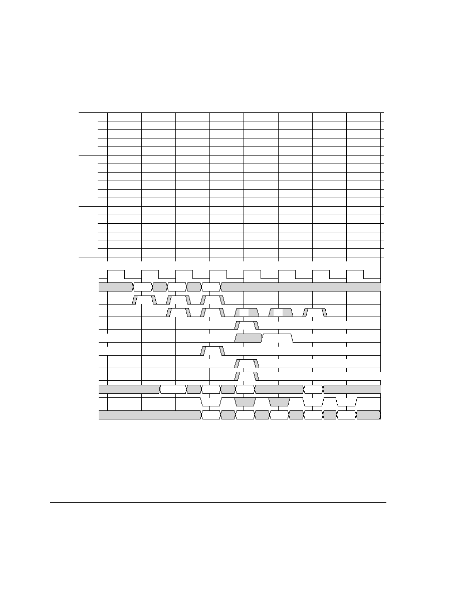
Coprocessor Interface
8-34
Copyright © 2001 ARM Limited. All rights reserved.
ARM DDI 0237A
Figure 8-14 I1 held up by ASTOPCPE and I2 held up by CPBUSYE
*Although instruction 2 is responsible for driving ASTOPCPD at T5, instruction 1 has
caused ASTOPCPE to be asserted and this has to be folded back into ASTOPCPD.
In Figure 8-15 on page 8-35, instruction 1 is held up by CPBUSYE and instruction 2 is
held up by ASTOPCPD.
I1
I1
I2
I1
I1
I2
I1
I2
I1
I3
I3
I
D
E
M
W
F
I
M
W
F
I
M
W
I2
I1
I3
I2
I3
I2
I3
I2
I3
I1
I1
I1
I1
I2
I3
I2
I3
I2
I3
I2
I3
I2
I3
I2
I3
ARM
CP1
CP2
D
E
D
E
T1
T2
T3
T4
T5
T6
T7
T8
1
3
2
3
2
1
3
3
2
1
3
1
2
2
2
3
1
2
2
3
2*
3
3
2
1
1
1
2
2
3
3
x
1
2
1
3
2
3
x
x
1
2
CPINSTR
CPINSTRV
CPCLK
CPVALIDD
CPBUSYE
CPLSLEN/
SWP/DBL
ASTOPCPE
CPBOUNCEE
STCMRCDATA
ASTOPCPD
CPBUSYE (internal)
HOLD E (internal)
2
1
1
2
3

Coprocessor Interface
ARM DDI 0237A
Copyright © 2001 ARM Limited. All rights reserved.
8-35
Figure 8-15 I1 held up by CPBUSYE and I2 held up by ASTOPCPD
*In Figure 8-15 although instruction 3 is responsible for driving ASTOPCPE at T7,
instruction 2 has caused ASTOPCPE to be asserted and this has to be folded back into
ASTOPCPD.
I1
I1
I2
I1
I1
I2
I1
I2
I1
I3
I3
I
D
E
M
W
F
I
M
W
F
I
M
W
I2
I1
I3
I1
I2
I3
I2
I3
I2
I3
I1
I1
I1
I1
I1
I2
I3
I2
I3
I2
I3
I2
I3
I2
I3
I2
I3
I2
ARM
CP1
CP2
D
E
D
E
T1
T2
T3
T4
T5
T6
T7
T8
CPCLK
CPINSTR
1
x
3
2
CPINSTRV
x
2
1
3
CPVALIDD
3
2
1
CPBUSYE
1
2
1
3
HOLD E (internal)
2
1
1
2
3
CPBUSYE (internal)
1
2
1
3
ASTOPCPD
3*
3
2
2
1
ASTOPCPE
1
1
2
2
3
CPLSLEN/
SWP/DBL
3
2
1
3
CPBOUNCEE
x
1
2
3
STCMRCDATA
3
2
1
x

Coprocessor Interface
8-36
Copyright © 2001 ARM Limited. All rights reserved.
ARM DDI 0237A
8.8.13
CPLSBUSY
This is driven out of a register on the CP Issue/Decode boundary (valid early in the
ARM10 Execute stage). It signals to other CPs that the sender is involved in a load or
store multiple data transfer and is keeping control of the STCMRCDATA bus. Other
CPs must progress to Decode (where they are stalled by ASTOPCPE) but must not
attempt to drive the bus until a cycle after CPLSBUSY deasserts.
CPLSBUSY stalls all other CPs when a long
LDC
is in progress. CPLSBUSY does not
have to go to the ARM10 processor because it can only do one load/store operation at
a time because they are held up in any case. CPLSBUSY comes out of flop and goes to
other CPs.
The CP drives CPLSBUSY in the CP Decode stage and the ARM10 Execute stage.
Table 8-14 CPLSBUSY interactions with other signals
Signal
Interactions with CPLSBUSY
ASTOPCPD
None
ASTOPCPE
None
LSHOLDCPE
None
LSHOLDCPM
None
ACANCELCP
None
AFLUSHCP
None
CPBOUNCEE
None

Coprocessor Interface
ARM DDI 0237A
Copyright © 2001 ARM Limited. All rights reserved.
8-37
8.9
Instruction cancelation
Instruction cancelation signals are described in the following sections:
∑
ACANCELCP
∑
ACANCELCP example
∑
ACANCELCP with ASTOPCPE example on page 8-39
∑
ACANCELCP with CPBUSYE example on page 8-40
∑
AFLUSHCP on page 8-41
∑
AFLUSHCP example on page 8-42.
8.9.1
ACANCELCP
ACANCELCP indicates that the instruction that has just entered the ARM10 Memory
stage must be canceled. ACANCELCP differs from AFLUSHCP. It cancels a single
instruction rather than canceling all upstream instructions in the pipeline. It is driven
from register following the ARM10 Execute stage. Table 8-15 shows ACANCELCP
the interactions with other signals.
The ARM10 processor drives ACANCELCP in the ARM10 Memory stage and the CP
Execute stage.
8.9.2
ACANCELCP example
ACANCELCP cancels one instruction (turns it into a NOP) but does not affect the ones
around it. In this case, three instructions are issued in a row. Instruction 2 is canceled.
Instructions 1 and 3 complete. The numbers in waveforms show which instruction owns
Table 8-15 ACANCELCP interactions with other signals
Signal
Interactions with CPBUSYE
ASTOPCPD
None
ASTOPCPE
CP ignores ACANCELCP if ASTOPCPE asserted
LSHOLDCPE
None
CPBUSYE
ACANCELCP is held is response to an active CPBUSYE
LSHOLDCPM
None
ACANCELCP
None
AFLUSHCP
AFLUSHCP has priority
CPBOUNCEE
No effect for canceled instructions

Coprocessor Interface
8-38
Copyright © 2001 ARM Limited. All rights reserved.
ARM DDI 0237A
the signal at that time. The ARM10 processor ignores an indication from CP2 that I2
must bounce as the instruction is canceled. Figure 8-16 shows an example with
ACANCELCP.
Figure 8-16 ACANCELCP example
The ARM10 processor ignores an indication from CP2 that instruction 2 must bounce
because the instruction is canceled.
I1
I1
I2
I1
I1
I2
I1
I2
I1
I3
I3
I
D
E
M
W
F
I
M
W
F
I
M
W
I1
I3
I3
I3
I1
I1
I1
I1
I2
I3
I2
I3
I2
I3
I2
I3
I3
ARM
CP1
CP2
D
E
D
E
T1
T2
T3
T4
T5
T6
T7
1
3
2
3
2
1
2
1
3
1
3
2
3
2
2
1
1
3
2
3
CPINSTR
CPINSTRV
CPCLK
CPVALIDD
ASTOPCPD
ASTOPCPE
CPBOUNCEE
ACANCELCP
3
3
1
2
CPLSLEN/
SWP/DBL
CPBUSYE
1
3
2
1

Coprocessor Interface
ARM DDI 0237A
Copyright © 2001 ARM Limited. All rights reserved.
8-39
8.9.3
ACANCELCP with ASTOPCPE example
Instruction 1 is held up by the ARM10 processor with ASTOPCPE. ACANCELCP is
valid in the last cycle that ASTOPCPE is asserted. Figure 8-17 shows an example of
ACANCELCP with ASTOPCPE.
Figure 8-17 ACANCELCP with ASTOPCPE example
2
I1
I1
I2
I1
I1
I2
I1
I1
I2
I
D
E
M
W
F
I
M
W
F
I
M
W
I1
I2
I2
I2
I1
I1
I1
I1
I2
I2
I2
I2
I2
I2
ARM
CP1
CP2
D
E
D
E
T1
T2
T3
T4
T5
T6
T7
1
2
2
1
2
1
1
2
2
1
1
1
2
CPINSTR
CPINSTRV
CPCLK
CPVALIDD
ASTOPCPD
ASTOPCPE
CPBOUNCEE
ACANCELCP
3
2
1
CPLSLEN/SWP/DBL
CPBUSYE
1
2
1
x
1
2
I1
I1
2

Coprocessor Interface
8-40
Copyright © 2001 ARM Limited. All rights reserved.
ARM DDI 0237A
8.9.4
ACANCELCP with CPBUSYE example
Instruction 1 is held up by CP1 as indicated by CPBUSYE. ACANCELCP is valid in
the last cycle that CPBUSYE is asserted.
ASTOPCPE might be asserted with CPBUSYE. It can then be deasserted while
CPBUSYE is still active or might have stayed asserted when CPBUSYE is deasserted.
When both CPBUSYE and ASTOPCPE are deasserted the pipeline must progress.
Figure 8-18 shows an example of ACANCELCP with CPBUSYE.
Figure 8-18 ACANCELCP with CPBUSYE example
2
I1
I1
I2
I1
I1
I2
I1
I1
I2
I
D
E
M
W
F
I
M
W
F
I
M
W
I1
I2
I2
I1
I1
I1
I1
I2
I2
I2
I2
I2
ARM
CP1
CP2
D
E
D
E
T1
T2
T3
T4
T5
T6
T7
1
2
2
1
2
1
1
2
1
x
1
1
2
CPINSTR
CPINSTRV
CPCLK
CPVALIDD
ASTOPCPD
ASTOPCPE
CPBOUNCEE
ACANCELCP
2
1
CPLSLEN/SWP/DBL
CPBUSYE
1
2
2
x
I1
x
1
1

Coprocessor Interface
ARM DDI 0237A
Copyright © 2001 ARM Limited. All rights reserved.
8-41
8.9.5
AFLUSHCP
AFLUSHCP indicates that the instruction that has just entered the ARM10 Memory
stage and all upstream instructions currently in the pipeline must be canceled.
AFLUSHCP differs from ACANCELCP because it cancels all upstream instructions
in the pipeline rather than just a single instruction. It is driven from register following
the ARM10 Execute stage. This means that there is no time to factor Data Aborts into
the AFLUSHCP signal. As a result, aborted CP loads complete when a Data Abort
occurs, and then be reexecuted on return from the Data Abort handler routine. It must
be possible to execute any CP load more than once (before the next instruction is
executed) with no noticeable effects on the CP.
The ARM10 processor drives AFLUSHCP in the ARM10 Memory stage and the CP
Execute stage.
AFLUSHCP supersedes the ASTOP and VALID signals from the ARM10 processor.
It is used to signal that an interrupt has flushed the pipeline. As a result CPBUSYE must
be deasserted in the following cycle to enable the interrupt to be serviced.
Table 8-16 AFLUSHCP interactions with other signals
Signal
Interactions with CPBUSYE
ASTOPCPD
Flush overrides
ASTOPCPE
Flush overrides
LSHOLDCPE
Flush overrides
CPBUSYE
Flush overrides (deasserted in the following cycle)
LSHOLDCPM
Flush overrides
ACANCELCP
None
CPBOUNCEE
Ignored because instruction canceled by flush

Coprocessor Interface
8-42
Copyright © 2001 ARM Limited. All rights reserved.
ARM DDI 0237A
8.9.6
AFLUSHCP example
AFLUSHCP has to override ASTOPCPE and ASTOPCPD. Here AFLUSHCP is
asserted for instruction 2. This might be caused by instruction 2 being bounced or a
reason unrelated to the CPs, an interrupt, for example. AFLUSHCP has to kill the
effects of instruction 2 and all following instructions currently in the pipe.
Interrupts can cause flushes at any time. So, even a valid instruction that has been
busy-waited for many cycles can be flushed. When the instruction has reached the
Memory stage of the ARM10 processor without AFLUSHCP or ACANCELCP being
asserted it completes (with the exception of instructions that Data Abort). Figure 8-19
on page 8-43 shows an example of this with five instructions. CP load or store
instructions that cause a Data Abort are completed by the CP and rerun by the Data
Abort handler. So they must be designed to be rerun with no ill effects.

Coprocessor Interface
ARM DDI 0237A
Copyright © 2001 ARM Limited. All rights reserved.
8-43
Figure 8-19 AFLUSHCP example
The ARM10 processor ignores an indication from CP2 that I2 might bounce as the
instruction is canceled. Instruction 4 might be in the Issue stage. This must be flushed
by AFLUSHCP but is also not confirmed by CPVALIDD. Instruction 5 is issued after
the flush and is a valid instruction.
AFLUSHCP can be asserted even if hold signals such as ACANCELCP and/or
CPBUSYE are asserted. In these cases, AFLUSHCP has the highest priority because
the pipe is currently full of instructions that do not execute. This might be because of a
mispredicted branch or an exception.
2
I1
I1
I2
I1
I1
I2
I1
I2
I3
I
D
E
M
W
F
I
M
W
F
I
M
W
I1
I1
I1
I1
I2
I3
I3
I3
ARM
CP1
CP2
D
E
D
E
T1
T2
T3
T4
T5
T6
T7
1
2
2
1
2
1
1
2
1
1
2
CPINSTR
CPINSTRV
CPCLK
CPVALIDD
ASTOPCPD
ASTOPCPE
CPBOUNCEE
AFLUSHCP
2
1
CPLSLEN/SWP/DBL
CPBUSYE
1
2
2
1
I1
3
2
T8
4
5
3
4
5
3
3
I3
I1
[I4]
I5
I2
I2
I4
I2
I5
3

Coprocessor Interface
8-44
Copyright © 2001 ARM Limited. All rights reserved.
ARM DDI 0237A
8.10
Bounced instructions
The following sections describe what happens when CPs cannot execute an instruction,
and the undefined instruction trap must be taken:
∑
CPBOUNCEE
∑
CPBOUNCEE example on page 8-45
∑
CPBOUNCEE with ASTOPCPE on page 8-46
∑
CPBOUNCEE with CPBUSYE on page 8-47.
8.10.1
CPBOUNCEE
CPBOUNCEE is used by CPs to acknowledge ownership of CP instructions. Only a
CP with an ID that matches the CPID field in the instruction can accept an instruction.
If no CP accepts an instruction, the instruction is bounced to an Undefined Instruction
handler, and the undefined instruction trap is taken. A CP does not have to accept all
instructions with an CPID that matches its ID. This allows a mixture of hardware and
software to be used to implement a CP.
The CP drives CPBOUNCEE out of a register at the start of the ARM10 Execute stage.
When an instruction is bounced, the CP should continue to operate as if it were a NOP.
If the bounced instruction passes its condition code check then the ARM10 processor
indicates that the CP should flush its pipeline using AFLUSHCP.
The CP that owns an instruction on the CPINSTR bus drives LOW the CPBOUNCEE
signal to the ARM10 processor in the CP Decode stage. If the instruction is not owned
by a CP, that CP leaves CPBOUNCEE HIGH. The ARM10 processor ANDs all
individual CPBOUNCEE signals internally. If CPBOUNCEE is HIGH across
ARM10 Execute/Memory boundary, the instruction is deemed to have not been
accepted by any CP, and the
UNDEFINED
instruction trap is taken. A CP may bounce an
instruction if the CP is unable to process that instruction or is unable to process a prior
instruction and requires software support.
The ARM10 processor ignores CPBOUNCEE if CPBUSYE is asserted and registers
the value of CPBOUNCEE at the end of the cycle that CPBUSYE deasserts. An active
ASTOPCPE does not prevent the value of CPBOUNCEE from being registered. If a

Coprocessor Interface
ARM DDI 0237A
Copyright © 2001 ARM Limited. All rights reserved.
8-45
CP is driving CPBUSYE, other CPs must hold CPBOUNCEE HIGH. The CP driving
CPBUSYE must hold its value of CPBOUNCEE until the cycle after CPBUSYE
deasserts.
8.10.2
CPBOUNCEE example
CPBPOUNCEE must only be considered valid in the last cycle where neither of
CPBUSYE or ASTOPCPE are asserted. Usually, AFLUSHCP is asserted following a
CPBOUNCEE. One case where this does not happen is when the bounced instruction
is canceled at the same time using ACANCELCP.
Here instruction 1 completes but instruction 2 bounces and might cause an
AFLUSHCP that cancels instruction 2 and instruction 3.
As long as one of them is HIGH at all times, CPBUSYE and ASTOPCPE can be
asserted and deasserted under each other multiple times while an instruction is held in
Execute. CPBOUNCEE is ignored until the first cycle in which both are not asserted.
Figure 8-20 on page 8-46 shows an example with CPBOUNCEE.
Table 8-17 CPBOUNCEE interactions with other signals
Signal
Interactions with CPBOUNCEE
ASTOPCPD
None
ASTOPCPE
The ARM10 processor registers CPBOUNCEE even if ASTOPCPE is
active
LSHOLDCPE
CPBOUNCEE is ignored until the cycle in which CPBUSYE deasserts
CPBUSYE
Flush overrides
LSHOLDCPM
None
ACANCELCP
A canceled, bounced instruction has no effect
CPBOUNCEE
Ignored as instruction canceled by flush

Coprocessor Interface
8-46
Copyright © 2001 ARM Limited. All rights reserved.
ARM DDI 0237A
Figure 8-20 CPBOUNCEE example
The flush can occur for a number of reasons. The undefined instruction trap is a low
priority exception.
8.10.3
CPBOUNCEE with ASTOPCPE
In Figure 8-21 on page 8-47 instruction 1 is held in the ARM10 Execute stage for one
cycle. CPBOUNCEE is only considered valid in the last cycle that ASTOPCPE is
asserted. So, in this case, instruction 1 does not bounce and instruction 2 does.
2
I1
I1
I2
I1
I1
I2
I1
I2
I3
I
D
E
M
W
F
I
M
W
F
I
M
W
I1
I1
I1
I1
I2
I3
I3
[I3]
ARM
CP1
CP2
D
E
D
E
T1
T2
T3
T4
T5
T6
T7
1
2
2
1
2
1
1
2
1
1
2
CPINSTR
CPINSTRV
CPCLK
CPVALIDD
ASTOPCPD
ASTOPCPE
CPBOUNCEE
AFLUSHCP
2
1
CPLSLEN/SWP/DBL
CPBUSYE
1
2
1
3
2
T8
3
3
3
I3
I1
I2
I2
[I2]
[I3]
[I2]
I1

Coprocessor Interface
ARM DDI 0237A
Copyright © 2001 ARM Limited. All rights reserved.
8-47
Figure 8-21 CPBOUNCEE with ASTOPCPE example
8.10.4
CPBOUNCEE with CPBUSYE
In Figure 8-22 on page 8-48 Instruction 1 is held in the ARM10 Execute stage for one
cycle. CPBOUNCEE is only considered valid in the last cycle that ASTOPCPE is
asserted. So, in this case instruction 1 does not bounce and instruction 2 does.
2
I1
I1
I2
I1
I1
I2
I1
I1
I2
I
D
E
M
W
F
I
M
W
F
I
M
W
I1
I1
I1
I2
I2
ARM
CP1
CP2
D
E
D
E
T1
T2
T3
T4
T5
T6
T7
1
2
2
1
2
1
1
2
1
1
2
CPINSTR
CPINSTRV
CPCLK
CPVALIDD
ASTOPCPD
ASTOPCPE
CPBOUNCEE
CPBOUNCEE (internal)
2
1
CPLSLEN/SWP/DBL
CPBUSYE
1
2
1
1
T8
I2
I2
I2
I1
I1
1
2
1
I2
I1
I1
I2
I2

Coprocessor Interface
8-48
Copyright © 2001 ARM Limited. All rights reserved.
ARM DDI 0237A
Figure 8-22 CPBOUNCEE with CPBUSYE example
I1
I1
I2
I1
I1
I2
I1
I1
I2
I
D
E
M
W
F
I
M
W
F
I
M
W
I1
I1
I1
I2
I2
ARM
CP1
CP2
D
E
D
E
T1
T2
T3
T4
T5
T6
T7
1
2
2
1
2
1
2
1
2
CPINSTR
CPINSTRV
CPCLK
CPVALIDD
ASTOPCPD
ASTOPCPE
CPBOUNCEE
CPBOUNCEE (internal)
2
1
CPLSLEN/SWP/DBL
CPBUSYE
1
2
1
1
T8
I2
I2
I2
I1
I1
1
I2
I1
I1
I2
I2
1
1
1
2

Coprocessor Interface
ARM DDI 0237A
Copyright © 2001 ARM Limited. All rights reserved.
8-49
8.11
Data buses
This section describes the 64-bit data buses:
∑
STCMRCDATA
∑
LDCMCRDATA on page 8-50.
8.11.1
STCMRCDATA
The 64-bit STCMRCDATA bus carries data from a CP to the ARM10 processor. For a
data transfer from a CP register to an ARM10 register (
MRC
) the data on
STCMRCDATA is written into a register in the ARM10 register bank. For a CP store
to memory (
STC
), the data on STCMRCDATA is passed though ARM10 processor to
the memory system. It is stored at an address generated by the ARM10 processor.
Table 8-18 describes the interactions between STCMRCDATA and signals.
STCMRCDATA is driven by a CP in the ARM10 Execute stage.
Table 8-18 STCMRCDATA interactions with signals
Signal
Interactions with STCMRCDATA
ASTOPCPD
None.
ASTOPCPE
The ARM10 processor registers the value on STCMRCDATA when
ASTOPCPE is asserted and the LSU pipeline and ALU pipeline are in
lockstep. If the pipelines are decoupled then ASTOPCPE only affects the
data processing operation that may be running under the loads or stores.
LSHOLDCPE
If the ALU and LSU pipelines are decoupled then ARM10 processor
registers the value on STCMRCDATA when LSHOLDCPE is asserted.
CPBUSYE
None.
LSHOLDCPM
None.
ACANCELCP
None.
CPBOUNCEE
None.

Coprocessor Interface
8-50
Copyright © 2001 ARM Limited. All rights reserved.
ARM DDI 0237A
8.11.2
LDCMCRDATA
The 64-bit LDCMCRDATA bus carries data from the ARM10 processor to a CP. For
a data transfer from an ARM10 register to a CP register (
MCR
), the data on
LDCMCRDATA is written into a register in the CP register bank. For a CP load from
memory (
LDC
), the data on LDCMCRDATA is passed though the ARM10 processor
from the memory system. It is loaded from an address generated by the ARM10
processor. Table 8-19 shows the interactions of LDCMRCDATA with other signals.
LDCMRCDATA is driven by the ARM10 processor in the ARM10 Write stage.
Table 8-19 LDCMRCDATA interactions with signals
Signal
Interactions with LDCMRCDATA
ASTOPCPD
None.
ASTOPCPE
None.
LSHOLDCPE
None.
CPBUSYE
None.
LSHOLDCPM
LSHOLDCPM indicates that the memory system did not return valid data
in the previous cycle. In this case there is not valid data on
LDCMCRDATA until LSHOLDCPM goes LOW.
ACANCELCP
None.
CPBOUNCEE
None.

ARM DDI 0237A
Copyright © 2001 ARM Limited. All rights reserved.
9-1
Chapter 9
JTAG Interface
This chapter describes the JTAG interface built into the ARM10 processor. It contains
the following sections:
∑
JTAG interface and halt mode on page 9-2
∑
JTAG instructions on page 9-4
∑
Scan chain descriptions on page 9-8.

JTAG Interface
9-2
Copyright © 2001 ARM Limited. All rights reserved.
ARM DDI 0237A
9.1
JTAG interface and halt mode
JTAG-based hardware debug using halt mode provides access to the integer unit and
debug logic. Access is through scan chains and the IEEE 1149.1 Test Access Port
(TAP). The TAP state machine is illustrated in Figure 9-1.
Figure 9-1 JTAG TAP state machine diagram
tms = 0
tms = 1
Test-Logic-Reset
0xF
tms = 0
Run-Test/Idle
0xC
Select-DR-Scan
0x7
Capture-DR
0x6
tms = 1
tms = 0
Shift-DR
0x2
tms = 0
Exit1-DR
0x1
tms = 1
tms = 0
Pause-DR
0x3
tms = 1
Exit2-DR
0x0
tms = 1
Update-DR
0x5
tms = 1
tms = 0
tms = 0
tms = 0
tms = 1
tms = 0
tms = 1
Select-IR-Scan
0x4
Capture-IR
0xE
Shift-IR
0xA
Exit1-IR
0x9
Pause-IR
0xB
Exit2-IR
0x8
Update-IR
0xD
tms = 1
tms = 0
tms = 0
tms = 0
tms = 0
tms = 1
tms = 1
tms = 1
tms = 1
tms = 1
tms = 0
tms = 1
tms = 0
tms = 1
tms = 1

JTAG Interface
ARM DDI 0237A
Copyright © 2001 ARM Limited. All rights reserved.
9-3
9.1.1
Entering debug state
Halt mode is enabled by writing a 1 to bit 30 of the Debug Status and Control Register
(DSCR). This can only be done by external debug hardware such as Multi-ICE. When
this mode is enabled, the processor halts, instead of taking an exception in software, if
one of the following events occurs:
∑
A HALT instruction has been scanned in through the JTAG interface. The TAP
controller must pass through Run-Test/Idle to issue the HALT command to the
ARM10 processor.
∑
An exception occurs and the corresponding vector catch enable bit is set.
∑
A register breakpoint hits.
∑
A watchpoint hits.
∑
A
BKPT
instruction reaches the Execute stage of the ARM10 pipeline.
∑
EDBGRQ is asserted.
Note
Software debug must not be used to debug abort and FIQ handlers. Setting a vector trap
on FIQ or a watchpoint or breakpoint anywhere in the vector table or handler code for
FIQs or aborts can lead to the abort handler being reentered before it has saved state.
The value in the abort mode link register and SPSR are overwritten and the information
required to return from the handler is lost.
The core halted bit in the DSCR is set when debug state is entered. At this point, the
debugger determines why the integer unit was halted and preserves the machine state.
The
MSR
instruction can be used to change modes and gain access to all banked registers
in the machine. While in debug state:
∑
the PC is not incremented
∑
external interrupts are ignored
∑
all instructions are read from the instruction transfer register (scan chain 4).
9.1.2
Exiting debug state
To exit from debug state, scan in the RESTART instruction through the JTAG interface.
The debugger might adjust the PC before restarting, depending on the way the integer
unit entered debug state. When the state machine enters the Run-Test/Idle state, normal
operations resume. The delay, waiting until the state machine is in Run-Test/Idle,
enables conditions to be set up in other devices in a multiprocessor system without
taking immediate effect. When Run-Test/Idle state is entered, all the processors resume
operation simultaneously. The core restarted bit is set when the RESTART sequence is
complete.The core halted bit DSCR0 is cleared before the core is restarted.

JTAG Interface
9-4
Copyright © 2001 ARM Limited. All rights reserved.
ARM DDI 0237A
9.2
JTAG instructions
The the JTAG interface portion of the logic implements the IEEE 1149.1 interface and
supports:
∑
a JTAG ID register
∑
a bypass register
∑
a 4-bit instruction register.
In addition, the public instructions listed in Table 9-1 are defined.
Note
All unused JTAG instructions default to the BYPASS instruction.
You can access the debug registers through either software, with
MCR
or
MRC
instructions, or through the JTAG interface port. See Chapter 10 Debug for details of
debug registers.
To write the CP14 registers R1, R4, and R5, use the EXTEST instruction. To read CP14
registers R0, R1, and R5, use the INTEST or EXTEXT instruction.
Table 9-1 Defined public JTAG instructions
Instruction Binary
code
Hexadecimal
code
EXTEST
0000
0x0
SCAN_N
0010
0x2
SAMPLE/PRELOAD
0011
0x3
RESTART
0100
0x4
CLAMP
0101
0x5
HIGHZ
0111
0x7
HALT
1000
0x8
CLAMPZ
1001
0x9
INTEST
1100
0xC
IDCODE
1110
0xE
BYPASS
1111
0xF

JTAG Interface
ARM DDI 0237A
Copyright © 2001 ARM Limited. All rights reserved.
9-5
SAMPLE/PRELOAD, CLAMP, HIGHZ, and CLAMPZ are applicable only to external
scan chains and they are not supported by scan chains in the ARM10 processor. These
instructions are not described in this document.
Note
The CP14 registers do not have interlocks. If the JTAG interface attempts to access a
CP14 register while the ARM10 processor is writing to it, the result is
UNPREDICTABLE
.
9.2.1
EXTEST
EXTEST connects the selected scan chain between TDI and TDO. Loading the
instruction register with the EXTEST instruction puts all the scan cells in their test
mode of operation.
In the Capture-DR state, inputs to the system logic are captured by the scan cells. In the
Shift-DR state, the previously captured test data is shifted out of the scan chain through
TDO, while new test data is shifted in through the TDI input. Data from the boundary
scan register cell is applied to the output pins in the Update-DR state. Typically, the first
test stimulus to be applied using the EXTEST instruction is shifted into the boundary
scan register using the SAMPLE/PRELOAD instruction.
Note
For debug, this instruction connects the selected scan chain between TDI and TDO.
When the instruction register is loaded with the EXTEST instruction, the debug scan
chains can be written.
Registers in CP14 that can be written by the JTAG interface, R1, R4, and R5, are written
using an EXTEST instruction.
9.2.2
SCAN_N
SCAN_N connects the scan path select register between TDI and TDO. During the
Capture-DR state, the fixed value 1000 is loaded into the register. During the Shift-DR
state, the ID number of the desired scan path is shifted into the scan path select register.
In the Update-DR state, the scan register of the selected scan chain is connected
between TDI and TDO, and remains connected until a subsequent SCAN_N instruction
is issued. On reset, scan chain 3 is selected by default.

JTAG Interface
9-6
Copyright © 2001 ARM Limited. All rights reserved.
ARM DDI 0237A
9.2.3
RESTART
RESTART is used to restart the processor on exit from debug state. The scan chain path
register is not affected and the processor exits debug state once the Run-Test/Idle state
is entered.
9.2.4
HALT
HALT stops the integer unit and puts it into debug state. The core can only be put into
debug state if debug halt mode is enabled.
9.2.5
INTEST
INTEST connects the selected scan chain between TDI and TDO. When the instruction
register is loaded with the INTEST instruction, all the scan cells are placed in their test
mode of operation.
This instruction enables serial testing of on-chip system logic by applying test stimuli.
The test results are captured and examined by shifting out the contents of the boundary
scan register. In the Capture-DR state, the value of the data applied from the integer unit
logic to the output scan cells and the value of the data applied from the system logic to
the input scan cells is captured.
In the Shift-DR state, the previously captured test data is shifted out of the scan chain
through the TDO pin.
Data is typically loaded into the parallel output register stages of the boundary scan
chain using the SAMPLE/PRELOAD instruction prior to its use.
Note
This instruction connects the selected scan chain between TDI and TDO. When the
instruction register is loaded with the INTEST instruction, the debug scan chains can be
read. INTEST is an optional instruction and its use is governed by the IEEE
1149.1-1990 standard and must be implemented according to those guidelines. In the
Capture-DR state, the value of the data applied from the integer unit logic to the output
scan cells and the value of the data applied from the system logic to the input scan cells
is captured. In the Shift-DR state, the previously captured test data is shifted out of the
scan chain through the TDO pin, while data shifted in through the TDI pin is ignored.
Registers R0, R1, and R5 are read with the INTEST instruction.

JTAG Interface
ARM DDI 0237A
Copyright © 2001 ARM Limited. All rights reserved.
9-7
9.2.6
IDCODE
IDCODE connects the device identification register, or ID register, between TDI and
TDO. The ID register is a 32-bit register that enables the manufacturer, part number,
and version of a component to be determined through the JTAG interface. When the
instruction register is loaded with the IDCODE instruction, all the scan cells are placed
in their normal (System) mode of operation.
In the Capture-DR state, the device identification code is captured by the ID register. In
the Shift-DR state, the previously captured device identification code is shifted out of
the ID register through the TDO pin, while data is shifted in through the TDI pin into
the ID register. In the Update-DR state, the ID register is unaffected.
See TAP ID register on page 9-9 for details of selecting and interpreting the ID register
value.
9.2.7
BYPASS
BYPASS connects a 1-bit shift register, the bypass register, between TDI and TDO.
When the BYPASS instruction is loaded into the instruction register, all the scan cells
are placed in their normal (System) mode of operation. This instruction has no effect on
the system pins.
In the Capture-DR state, a logic 0 is captured by the bypass register. In the Shift-DR
state, test data is shifted into the bypass register through TDI and out through TDO after
a delay of one TCK cycle. The bypass register is not affected in the Update-DR state.
The first bit shifted out is a zero.
All unused JTAG instruction codes default to the BYPASS instruction.

JTAG Interface
9-8
Copyright © 2001 ARM Limited. All rights reserved.
ARM DDI 0237A
9.3
Scan chain descriptions
This section describes the following scan chains:
∑
BYPASS register
∑
TAP ID register on page 9-9
∑
Instruction register on page 9-10
∑
Scan chain select register on page 9-10
∑
Scan chain 0, debug ID register on page 9-11
∑
Scan chain 1, debug status and control register (DSCR) on page 9-11
∑
DSCR readable and writable bits on page 9-14
∑
Scan Chain 2 on page 9-15
∑
Scan Chain 3 on page 9-15
∑
Scan Chain 4 on page 9-15
∑
Scan chain 5, CP14 R5 on page 9-16
∑
Scan chain 6 on page 9-16.
9.3.1
BYPASS register
Purpose
Bypasses the device during scan testing by providing a path between TDI
and TDO.
Length
1 bit
Operating
mode
When the bypass instruction is the current instruction in the instruction
register, serial data is transferred from TDI to TDO in the Shift-DR state
with a delay of one TCK cycle. There is no parallel output from the
bypass register. A logic 0 is loaded from the parallel input of the bypass
register in Capture-DR state.
Order
TDI-[0]-TDO

JTAG Interface
ARM DDI 0237A
Copyright © 2001 ARM Limited. All rights reserved.
9-9
9.3.2
TAP ID register
Purpose
The TAP controller ID of each core type is unique. The JTAG ID of this
ARM10 processor is initially
0x14A20F0F
. A JTAG debugger such as
Multi-ICE can easily identify the processor. The JTAG ID register is
routed to the edge of the chip so that partners can create their own ID
numbers by tying the pins to HIGH or LOW values. Partner-specific
devices are identified by ID numbers of the form shown in Figure 9-2.
Figure 9-2 TAP ID register
Length
32 bits
Version
Bits[31:28]
Part Number
Bits [27:12]
Manufacturer ID Bits [11:1]
LSB
Bit 0
Operating mode
When the IDCODE instruction is current, the TAP ID register is
selected as the serial path between TDI and TDO. There is no
parallel output from the TAP ID register. The 32-bit ID code is
loaded into the register from its parallel inputs during the
Capture-DR state.
Order
TDI-[31, 30]...[1, 0]-TDO
LSB
0
Part number
Manufacturer ID
Version
31
28 27
12 11
1

JTAG Interface
9-10
Copyright © 2001 ARM Limited. All rights reserved.
ARM DDI 0237A
9.3.3
Instruction register
Purpose
Holds the current TAP instruction.
Length
4 bits
Operating mode
When in Capture-DR state, the instruction register is selected as
the serial path between TDI and TDO. During the Capture-DR
state, the value b0001 is loaded into this register. This is shifted
out during Shift-IR, least significant bit first, while a new
instruction is shifted in, least significant bit first. During the
Update-IR state, the value in the instruction register becomes the
current instruction. On reset, IDCODE becomes the current
instruction. The value of the current instruction is reflected on the
IR[3:0] output bus.
Order
TDI - 3, 2, 1, 0 - TDO
9.3.4
Scan chain select register
Purpose
Holds the current active scan chain.
Length
5 bits
Operating mode
After SCAN_N has been selected as the current instruction, when
in Shift-DR state, the scan chain select register is selected as the
serial path between TDI and TDO. During the Capture-DR state,
binary 10000 is loaded into this register. This is shifted out during
Shift-DR, least significant bit first, while a new value is shifted in,
least significant bit first. During the Update-DR state, the value in
the register selects a scan chain to become the currently active
scan chain. All further instructions such as INTEST then apply to
that scan chain. The currently selected scan chain only changes
when a SCAN_N instruction is executed, or a reset occurs. On
reset, scan chain 3 is selected as the active scan chain. The number
of the currently selected scan chain is reflected on the
SCREG[4:0] output bus. The TAP controller can be used to
control external scan chains in addition to those within the
ARM10 processor. The external scan chain must be assigned a
number and control signals must be generated for it. The number
and control signals can be derived from SCREG[4:0], IR[3:0],
TAPSM[3:0], and TCK.
Order
TDI - 4, 3, 2, 1, 0 - TDO

JTAG Interface
ARM DDI 0237A
Copyright © 2001 ARM Limited. All rights reserved.
9-11
9.3.5
Scan chain 0, debug ID register
Purpose
Debug. This scan chain is CP14 R0, the debug ID register. The
debug ID register value is
0x41006201
.
Length
32 bits
Order
TDI - 31, 30, 29, . . . 2, 1, 0 - TDO
9.3.6
Scan chain 1, debug status and control register (DSCR)
Purpose
Debug. This scan chain is CP14 R1, the DSCR.
Length
32 bits
Defined bits
The following bits are defined for Chain 1:
DSCR0
Core halted.
DSCR1
Core restarted.
DSCR[4:2]
Method of debug entry. Table 9-2 shows the method of entry bit
values.
DSCR5
Abort occurred. This is writable only with an
MCR
to CP14 register
1. This bit is sticky. It is cleared with an
MCR
to the DSCR where
this bit is written as a zero. Reset when NTRST = 0 or if the TAP
controller is in the reset state.
Table 9-2 Method of debug entry bit values
DSCR[4:2]
Meaning
000
JTAG HALT instruction occurred
001
Breakpoint occurred
010
Watchpoint occurred
011
BKPT
instruction occurred
100
External debug request occurred
101
Vector catch occurred
110
Data-side abort occurred
111
Instruction-side abort occurred

JTAG Interface
9-12
Copyright © 2001 ARM Limited. All rights reserved.
ARM DDI 0237A
DSCR6
wDTR buffer empty. This bit indicates to the core that the wDTR
buffer is empty, meaning that the core can write more data into it.
This is the inversion of the bit that the JTAG debugger sees if it
polls the DTR by going through Capture-DR with EXTEST. The
debugger must not use this bit to determine if the wDTR is empty
or full because the timing between the JTAG interface signal and
the core signal is different.
DSCR7
rDTR buffer full. This bit indicates to the core that the rDTR
buffer is full, meaning that the debugger has written data into it.
This is the inversion of the bit that the JTAG debugger sees if it
polls the DTR by going through CaptureDR with INTEST. The
debugger must not use this bit to determine if the rDTR is empty
or full because the timing between the JTAG interface signal and
the core signal is different.
DSCR[15:8]
Reserved.
DSCR16
Vector catch enable, Reset.
Reset when NTRST = 0 or if the TAP controller is in the Reset
state.
DSCR17
Vector catch enable, undefined instruction.
Reset when NTRST = 0 or if the TAP controller is in the Reset
state.
DSCR18
Vector catch enable, SWI.
Reset when NTRST = 0 or if the TAP controller is in the Reset
state.
DSCR19
Vector catch enable, Prefetch Abort.
Reset when NTRST = 0 or if the TAP controller is in the Reset
state.
DSCR20
Vector catch enable, Data Abort.
Reset when NTRST = 0 or if the TAP controller is in the Reset
state.
DSCR21
Reserved.
DSCR22
Vector catch enable, IRQ.
Reset when NTRST = 0 or if the TAP controller is in the Reset
state.

JTAG Interface
ARM DDI 0237A
Copyright © 2001 ARM Limited. All rights reserved.
9-13
DSCR23
Vector catch enable, FIQ.
Reset when NTRST = 0 or if the TAP controller is in the Reset
state.
DSCR[26:24]
Reserved.
DSCR27
Comms Channel Mode:
1 = comms channel activity.
0 = no comms channel activity
Reset when NTRST = 0 or if the TAP controller is in the Reset
state.
DSCR28
Thumb state indicator (see Table 10-5 on page 10-7).
Thumb instruction:
1 = ITR contains a Thumb instruction.
0 = ITR contains an ARM instruction
DSCR29
Execute instruction in ITR select:
1 = instruction in ITR is sent to prefetch unit if JTAG state
machine passes through Run-Test/Idle.
0 = disabled
Set when NTRST = 0 or if the TAP controller is in the Reset state.
DSCR30
Halt/Monitor mode select:
1 = halt mode enabled.
0 = monitor mode enabled
Reset when NTRST = 0 or if TAP controller is in Reset state.
DSCR31
Global debug enable:
1 = all debugging functions enabled.
0 = all debugging functions disabled (breakpoints and
watchpoints)
Reset when NRESET = 0 (the core Reset line).

JTAG Interface
9-14
Copyright © 2001 ARM Limited. All rights reserved.
ARM DDI 0237A
9.3.7
DSCR readable and writable bits
The DSCR can be seen from core and from the JTAG interface. The readable and
writable bits seen from the core and the JTAG debugger are summarized in Table 9-3.
Note
The comms channel bits, rDTRFull and wDTREmpty, are inversions of what the
debugger sees, because these bits are mirrored in the DSCR for the core, not the
debugger.
Order
TDI - 31, 30 . . . 1, 0 - TDO
Table 9-3 DSCR bits from the core
DSCR bits
View from core
View from JTAG
[1:0]
Reserved
Read-only
[4:2]
Read-only
Read-only
5
Reserved
Read-only
[7:6]
Read-only
Read-only
[15:8]
Reserved
Reserved
[23:16]
Read-only
Readable/writable
[26:24]
Reserved
Reserved
[30:27]
Reserved
Readable/writable
31
Readable/writable
Read-only

JTAG Interface
ARM DDI 0237A
Copyright © 2001 ARM Limited. All rights reserved.
9-15
9.3.8
Scan Chain 2
Scan chain 2 is the combination of scan chain 4 and scan chain 5. Scan chain 4 is the
Instruction Transfer Register, ITR, and scan chain 5 is the Data Transfer Register,
DTR. The instruction complete bit, ITR0, is not included in this combination. It appears
only in scan chain 4.
Figure 9-3 Scan chain 2
9.3.9
Scan Chain 3
Purpose
Can be used for external boundary scan testing. Used for
interdevice testing (EXTEST) and testing the core (INTEST).
Length
Undetermined
9.3.10
Scan Chain 4
Purpose
Debug
Length
33 bits
Purpose
This scan chain is the Instruction Transfer Register (ITR), used to
send instructions to the core through the prefetch unit. This chain
consists of 32 bits of information, plus an additional bit to indicate
the completion of the instruction sent to the core. Instructions
scanned into the ITR are not executed unless the instruction
transfer execute bit DSCR29 is asserted. Bit 0 indicates if the
instruction in the ITR has completed execution.
Order
TDI-[32, 31, 30]...[1, 0]-TDO
64
63
62
ITR32
0
2
1
35
34
33
32
36
. . .
ITR31 ITR30
DTR0 TDO
TDI
DTR1
DTR2
. . .
ITR1
ITR2
ITR3
DTR32 DTR31

JTAG Interface
9-16
Copyright © 2001 ARM Limited. All rights reserved.
ARM DDI 0237A
9.3.11
Scan chain 5, CP14 R5
CP14 is the Data Transfer Register, DTR. It consists of two separate registers, the
read-only rDTR and the write-only wDTR. The two registers facilitate the creation of a
bidirectional comms channel in software.
The rDTR can be loaded only through the JTAG port and is read-only by the core using
an
MRC
instruction. The rDTR chain contains 32 bits of information plus one additional
bit for the comms channel.
The wDTR can be loaded only by the core through an
MCR
instruction and is read-only
through the JTAG port. The wDTR contains 32 bits of information plus one additional
bit for the comms channel. The definition of bit 0 depends on whether the current JTAG
instruction is INTEST or EXTEST. If the current instruction is EXTEST, the debugger
can write to the rDTR, and bit 0 indicates if there is still valid data in the queue. If the
bit is set, the debugger can write new data. When the core performs a read of the rDTR,
bit 0 is automatically asserted. Conversely, if the JTAG instruction is INTEST, bit 0
indicates if there is currently valid data to read in the wDTR. If the bit is set, the JTAG
interface must read the contents of the wDTR, which in turn, clears the bit. The core can
then sample its own wDTR empty bit and write new data for the debugger.
The TAP controller see either rDTR or wDTR depending on the instruction only sees
one register through scan chain 5, and the appropriate register is chosen depending on
which instruction is used (INTEST or EXTEST).
Purpose
Debug.
Length
33 bits.
Order
TDI-rDTR[32]rDTR[31]...rDTR[1]rDTR[0]
wDTR[32]wDTR[31]...wDTR[1]wDTR[0]-TDO
9.3.12
Scan chain 6
Purpose
ETM
Length
40 bits
Purpose
The ETM scan chain. Refer to Embedded Trace Macrocell
Technical Reference Manual.

ARM DDI 0237A
Copyright © 2001 ARM Limited. All rights reserved.
10-1
Chapter 10
Debug
This chapter describes the debug unit. These features assist the development of
application software, operating systems, and hardware. This chapter contains the
following sections:
∑
About the debug unit on page 10-2
∑
Register descriptions on page 10-5
∑
Software lockout function on page 10-15
∑
Halt mode on page 10-16
∑
Monitor mode on page 10-19
∑
Values in the link register after aborts on page 10-20
∑
Comms channel on page 10-21.

Debug
10-2
Copyright © 2001 ARM Limited. All rights reserved.
ARM DDI 0237A
10.1
About the debug unit
The debug unit assists in debugging software. The debug hardware, in combination with
a software debugger program, can be used to debug:
∑
application software
∑
operating systems
∑
ARM10-based hardware systems.
The debug unit enables you to:
∑
stop program execution
∑
examine and alter processor and coprocessor state
∑
examine and alter memory and input/output peripheral state
∑
restart the processor core.
The debug unit provides several ways to stop execution. The most common is for
execution to halt when a particular memory address is accessed, either for an instruction
fetch (a breakpoint), or a data access (a watchpoint). When execution has stopped, one
of two modes is entered:
Halt mode
All processor execution halts, and can only be restarted with
hardware connected to the external JTAG interface. You can
examine and alter all processor state (CPU registers), coprocessor
state, memory, and input/output locations through the JTAG
interface. This mode is intentionally invasive to program
execution. In halt mode you can debug the processor irrespective
of its internal state. Halt mode requires external hardware to
control the JTAG interface. A software debugger provides the user
interface to the debug hardware.
Monitor mode
In monitor mode the processor stops execution of the current
program and starts execution of a Debug Abort handler. The state
of the processor is preserved in the same manner as all ARM
exceptions (see The ARM Architecture Reference Manual on
exceptions and exception priorities). The abort handler
communicates with a debugger application to access processor
and coprocessor state, and to access memory contents and
input/output peripherals. Monitor mode requires a debug monitor
program to interface between the debug hardware and the
software debugger.

Debug
ARM DDI 0237A
Copyright © 2001 ARM Limited. All rights reserved.
10-3
10.1.1
Halt mode and monitor mode compared
Halt mode is for nonreal-time debugging. Because of its hardware nature, you can use
halt mode to debug the processor under almost all circumstances. However, real-time
systems in which processor execution cannot be completely suspended are unlikely to
be able to tolerate the intrusion caused by halt mode. Therefore monitor mode is
provided for time-critical applications that cannot tolerate a long interruption while the
processor is halted. Monitor mode relies on the processor being able to freely execute
instructions to process debug requests.
10.1.2
Programming the debug unit
The debug unit is programmed using Coprocessor 14, CP14. CP14 provides:
∑
instruction address comparators for triggering breakpoints
∑
data address comparators for triggering watchpoints
∑
a bidirectional serial communication channel
∑
all other state information associated with debug.
CP14 is accessed using coprocessor instructions in both halt mode and monitor mode.
BKPT
instructions cause a Prefetch Abort if debug is disabled.
10.1.3
Summary of CP14 registers
All debug state is mapped into CP14 as registers. Three CP14 registers, R0, R1, and R5,
can be accessed by software running on the processor. Four registers, R0, R1, R4, and
R5, are accessible as scan chains from the JTAG interface. R4, the instruction transfer
register, is accessible only as a scan chain. The remaining registers are accessible only
by software operating in a privileged processor mode. Table 10-1 shows the CP14
registers and their scan chain numbers.
Table 10-1 CP14 registers and scan chain numbers
Register
Register name
Scan chain number
CP14 R0
Debug ID register, DIDR
0
CP14 R1
Debug Status and Control Register, DSCR
1
CP14 R2 and R3
Reserved
-
CP14 R4
Instruction Transfer Register, ITR
4
CP14 R5
Data Transfer Register, DTR
5
CP14 R6-R63
Reserved
-

Debug
10-4
Copyright © 2001 ARM Limited. All rights reserved.
ARM DDI 0237A
The register file has space reserved for up to 16 breakpoints and 16 watchpoints. A
particular implementation can have any number from 2 to 16. The processor has six
instruction-side breakpoints and two data-side watchpoints.
There are two requirements to enable debugging:
∑
An enable bit in the debug status and control register enables debug functionality
through software. Reset clears the enable bit, disabling all debug functionality.
The processor ignores external debug requests, and
BKPT
instructions cause
Prefetch Aborts. In this mode, an operating system can quickly enable and disable
debugging on individual tasks as part of the task-switching sequence.
∑
The DBGEN pin allows the debug features of the processor to be disabled
entirely.
The DBGEN pin must be tied HIGH to enable the debug functionality of the core.
DBGEN must be tied LOW only when debugging is never required.
The
CRm
and
opcode2
fields are used to encode the debug register number, where the
register number is {
opcode2
,
CRm
}.
CP14 R64-R69
Breakpoint Address registers, BA0-BA5
-
CP14 R70-R79
Reserved
-
CP14 R80-R85
Breakpoint Control registers, BC0-BC5
-
CP14 R86-R95
Reserved
-
CP14 R96 and R97
Watchpoint Address registers, WA0 and WA1
-
CP14 R112 and R113
Watchpoint Control registers, WC0 and WC1
-
CP14 R114 and R127
Reserved
-
Table 10-1 CP14 registers and scan chain numbers (continued)
Register
Register name
Scan chain number

Debug
ARM DDI 0237A
Copyright © 2001 ARM Limited. All rights reserved.
10-5
10.2
Register descriptions
This section describes the CP14 registers:
∑
CP14 R0, debug ID register
∑
CP14 R1, debug status and control register on page 10-6
∑
CP14 R2-R4 on page 10-8
∑
CP14 R5, data transfer register on page 10-8
∑
CP14 R6-R63 on page 10-9
∑
CP14 R64-R69, breakpoint address registers on page 10-9
∑
CP14 R70-R79 on page 10-10
∑
CP14 R80-R85, breakpoint control registers on page 10-10
∑
CP14 R86-R95 on page 10-11
∑
CP14 R96 and R97, watchpoint address registers on page 10-12
∑
CP14 R112 and R113, watchpoint control registers on page 10-13
∑
CP14 R114-R127 on page 10-14
10.2.1
CP14 R0, debug ID register
The Debug ID Register, DIDR, is read-only and contains
0x41006201
. Table 10-2 shows
the instructions for reading DIDR.
Figure 10-1 shows the DIDR bit fields.
Figure 10-1 Debug ID register
Table 10-2 Debug ID register instructions
Instruction
Description
MRC p14,0,Rd,c0,c0,0
Copies contents of debug ID register into Rd.
31
24
15
12
7
4 3
0
Revision
0001
SBZ
0000
Watchpoints
0010
Breakpoints
0110
SBZ
0000
Architecture
0000
Designer code
0100 0001
23
20 19
16
11
8

Debug
10-6
Copyright © 2001 ARM Limited. All rights reserved.
ARM DDI 0237A
Table 10-3 describes the DIDR bit fields.
10.2.2
CP14 R1, debug status and control register
The Debug Status and Control Register, DSCR, is a read/write register. Table 10-4
shows the instructions for accessing DSCR.
Figure 10-2 shows the DSCR bit fields.
Figure 10-2 Debug status and control register
Table 10-3 Encoding of the debug ID register
Bits
Meaning
[31:24]
Designer code
[23:20]
SHOULD BE ZERO
[19:16]
Debug architecture version
[15:12]
Number of implemented register breakpoints
[11:8]
Number of implemented watchpoints
[7:4]
SHOULD BE ZERO
[3:0]
Revision number
Table 10-4 Debug status and control register instructions
Instruction
Description
MRC p14,0,Rd,c0,c1,0
Copies contents of debug status and control register into Rd.
MCR p14,0,Rd,c0,c1,0
Copies contents of Rd into debug status and control register.
31 30 29 28 27
24 23 22 21 20 19 18 17 16
1
0
CF C1
Reserved
GE H E T
MOE
Reserved
CR
CP CS CU
R CD
Reserved
7
6 5
RF WE R
2
4
15
8

Debug
ARM DDI 0237A
Copyright © 2001 ARM Limited. All rights reserved.
10-7
Table 10-5 describes the DSCR bit fields.
Table 10-5 Encoding of debug status and control register
Bits
Definition
31
GE, global debug enable bit. Reset clears GE.
1 = All debugging functions enabled
0 = All debugging functions disabled.
30
H, halt mode bit. Reset clears H.
1 = halt mode
0 = monitor mode.
29
E, execute bit.
1 = execute instruction in ITR when in JTAG Run-Test/Idle state
0 = do not execute instruction in ITR when in JTAG Run-Test/Idle state.
28
T, Thumb instruction bit:
1 = ITR contains a Thumb instruction
0 = ITR contains an ARM instruction.
[27:24]
Reserved.
DSCR[23:22] and DSCR[20:16] are used to catch ARM exceptions. The effect of setting one
of these bits is the same as setting a register breakpoint on the address of the exception vector.
23
CF, vector catch FIQ bit; read-only.
22
CI, vector catch IRQ bit; read-only.
21
Reserved.
20
CD, vector catch Data Abort bit; read-only.
19
CP, vector catch Prefetch Abort bit; read-only.
18
CS, vector catch Software Interrupt bit; read-only.
17
CU, vector catch Undefined Instruction bit; read-only.
16
CR, vector catch reset bit; read-only.
[15:8]
Reserved.
7
RF, rDTR buffer full bit; read-only:
1 = new data placed in the rDTR through the JTAG interface that can be read with
a
MRC
or
STC
instruction
0 = no new data placed in the rDTR through the JTAG interface.

Debug
10-8
Copyright © 2001 ARM Limited. All rights reserved.
ARM DDI 0237A
10.2.3
CP14 R2-R4
CP14 R2-R4 are reserved.
10.2.4
CP14 R5, data transfer register
The Data Transfer Register, DTR, is a read/write register. Table 10-6 shows the
instructions for accessing DTR.
Figure 10-3 on page 10-9 shows the DTR bit field.
6
WE, wDTR buffer empty bit; read-only:
1 = the wDTR buffer is ready to have data written to it
0 = data has not been read through the JTAG interface
5
-
[4:2]
MOE, method of entry bits; read-only:
000 = JTAG halt instruction
001 = breakpoint hit
010 = watchpoint hit
011 = breakpoint instruction requested
100 = external debug requested asserted
101 = vector catch occurred
110 = data-side abort occurred
111 = instruction-side abort occurred
[1:0]
-
Table 10-5 Encoding of debug status and control register (continued)
Bits
Definition
Table 10-6 Data transfer register instructions
Instruction
Description
MRC p14,0,Rd,c0,c5,0
Copies contents of DTR into Rd.
MCR p14,0,Rd,c0,c5,0
Copies contents of Rd into DTR.
LDC p14,c5,<addressing mode>
Loads value accessed in memory into DTR.
STC p14,c5,<addressing mode>
Stores contents of DTR to memory.

Debug
ARM DDI 0237A
Copyright © 2001 ARM Limited. All rights reserved.
10-9
Figure 10-3 Data transfer register
Note
Physically, the DTR is two separate registers, the rDTR for reading and the wDTR for
writing.
10.2.5
CP14 R6-R63
CP14 R6-R63 are reserved.
10.2.6
CP14 R64-R69, breakpoint address registers
The Breakpoint Address registers, BA0-5, are read/write registers. Table 10-7 shows the
instructions for accessing BA0-5.
31
0
Transfer data
Table 10-7 Breakpoint address register instructions
Register
Instruction
Description
CP14 R64, BA0
MRC p14,0,Rd,c0,c0,4
Copies contents of BA0 into Rd
MCR p14,0,Rd,c0,c0,4
Copies contents of Rd into BA0
CP14 R65, BA1
MRC p14,0,Rd,c0,c1,4
Copies contents of BA1 into Rd
MCR p14,0,Rd,c0,c1,4
Copies contents of Rd into BA1
CP14 R66, BA2
MRC p14,0,Rd,c0,c2,4
Copies contents of BA2 into Rd
MCR p14,0,Rd,c0,c2,4
Copies contents of Rd into BA2
CP14 R67, BA3
MRC p14,0,Rd,c0,c3,4
Copies contents of BA3 into Rd
MCR p14,0,Rd,c0,c3,4
Copies contents of Rd into BA3
CP14 R68, BA4
MRC p14,0,Rd,c0,c4,4
Copies contents of BA4 into Rd
MCR p14,0,Rd,c0,c4,4
Copies contents of Rd into BA4
CP14 R69, BA5
MRC p14,0,Rd,c0,c5,4
Copies contents of BA5 into Rd
MCR p14,0,Rd,c0,c5,4
Copies contents of Rd into BA5
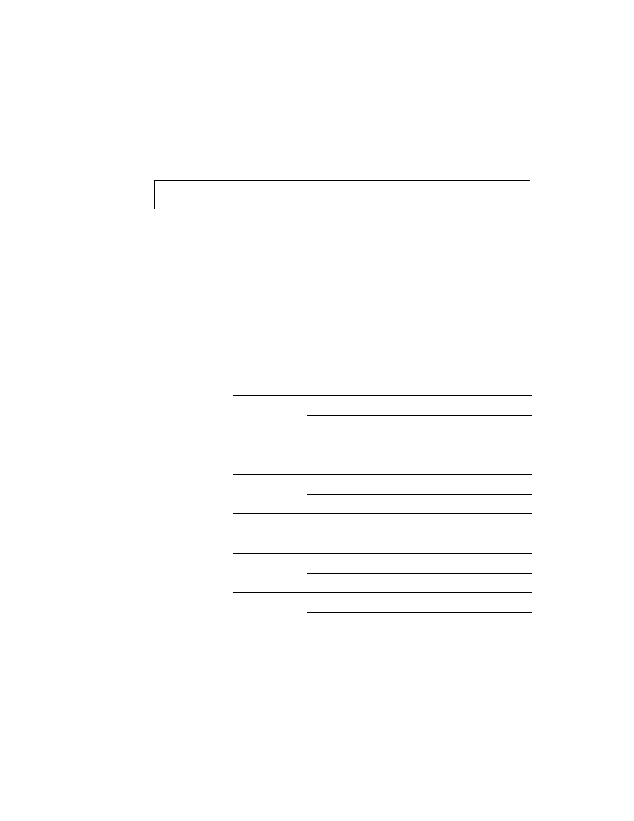
Debug
10-10
Copyright © 2001 ARM Limited. All rights reserved.
ARM DDI 0237A
Figure 10-4 shows the BA0-5 bit field.
Figure 10-4 Breakpoint address registers
10.2.7
CP14 R70-R79
CP14 R70-R79 are reserved.
10.2.8
CP14 R80-R85, breakpoint control registers
The Breakpoint Control registers, BC0-5, are read/write registers. Table 10-8 shows the
instructions for accessing BC0-5.
Figure 10-5 on page 10-11 shows the BC0-5 bit fields.
31
0
Breakpoint address
Table 10-8 Breakpoint control register instructions
Register
Instruction
Description
CP14 R80, BC0
MRC p14,0,Rd,c0,c0,5
Copies contents of BC0 into Rd
MCR p14,0,Rd,c0,c0,5
Copies contents of Rd into BC0
CP14 R81, BC1
MRC p14,0,Rd,c0,c1,5
Copies contents of BC1 into Rd
MCR p14,0,Rd,c0,c1,5
Copies contents of Rd into BC1
CP14 R82, BC2
MRC p14,0,Rd,c0,c2,5
Copies contents of BC2 into Rd
MCR p14,0,Rd,c0,c2,5
Copies contents of Rd into BC2
CP14 R83, BC3
MRC p14,0,Rd,c0,c3,5
Copies contents of BC3 into Rd
MCR p14,0,Rd,c0,c3,5
Copies contents of Rd into BC3
CP14 R84, BC4
MRC p14,0,Rd,c0,c4,5
Copies contents of BC4 into Rd
MCR p14,0,Rd,c0,c4,5
Copies contents of Rd into BC4
CP14 R85, BC5
MRC p14,0,Rd,c0,c5,5
Copies contents of BC5 into Rd
MCR p14,0,Rd,c0,c5,5
Copies contents of Rd into BC5

Debug
ARM DDI 0237A
Copyright © 2001 ARM Limited. All rights reserved.
10-11
Figure 10-5 Breakpoint control registers
Table 10-9 describes the BC0-5 bit fields.
10.2.9
CP14 R86-R95
CP14 R86-R95 are reserved.
E
0
SA
IT
SBZ
31
5 4 3 2 1
Table 10-9 Encoding of breakpoint control registers
Bit
Name
Definition
[31:5]
-
SHOULD BE ZERO
.
[4:3]
IT
Instruction type bit:
00 = reserved
10 = ARM instruction
01 = Thumb instruction
11 = either
[2:1]
SA
Supervisor access bit:
00 = reserved
10 = privileged
01 = user
11 = either
0
E
Enable bit. Reset clears E:
0 = register disabled
1 = register enabled

Debug
10-12
Copyright © 2001 ARM Limited. All rights reserved.
ARM DDI 0237A
10.2.10 CP14 R96 and R97, watchpoint address registers
The Watchpoint Address registers, WA0 and WA1, are read/write registers. Table 10-10
shows the instructions for accessing WA0 and WA1.
Figure 10-6 shows the watchpoint address bit field.
Figure 10-6 Watchpoint address registers
Table 10-10 Watchpoint address register instructions
Register
Instruction
Description
CP14 R96, WA0
MRC p14,0,Rd,c0,c0,6
Copies contents of WA0 into Rd
MCR p14,0,Rd,c0,c0,6
Copies contents of Rd into WA0
CP14 R97, WA1
MRC p14,0,Rd,c0,c1,6
Copies contents of WA1 into Rd
MCR p14,0,Rd,c0,c1,6
Copies contents of Rd into WA1
31
0
Watchpoint address

Debug
ARM DDI 0237A
Copyright © 2001 ARM Limited. All rights reserved.
10-13
10.2.11 CP14 R112 and R113, watchpoint control registers
The Watchpoint Control registers, WC0 and WC1, are read/write registers. Table 10-11
shows the instructions for accessing WC0 and WC1.
Figure 10-7 shows the WC0 and WC1 bit fields.
Figure 10-7 Watchpoint control registers
Table 10-12 describes the WC0 and WC1 bit fields.
Table 10-11 Watchpoint control register instructions
Register
Instruction
Description
R112, WC0
MRC p14,0,Rd,c0,c0,7
Copies contents of WC0 into Rd
MCR p14,0,Rd,c0,c0,7
Copies contents of Rd into WC0 control
R113, WC1
MRC p14,0,Rd,c0,c1,7
Copies contents of WC1 into Rd
MCR p14,0,Rd,c0,c1,7
Copies contents of Rd into WC1
E
8
0
L/S/E
S
S
Size
Mask
SBZ
31
11
7
5 4 3
10 9
2 1
Table 10-12 Encoding of watchpoint control registers
Bits
Definition
[31:11]
SHOULD BE ZERO
.
[10:9]
DA[1:0] address mask.
Bit 10:
1 = exclude DA1 in comparison
0 = include DA1 in comparison
Bit 9:
1 = exclude DA0 in comparison
0 = include DA0 in comparison
8
SHOULD BE ZERO
.

Debug
10-14
Copyright © 2001 ARM Limited. All rights reserved.
ARM DDI 0237A
10.2.12 CP14 R114-R127
R114-R127 are reserved.
[7:5]
Byte/halfword/word/any size:
000 = reserved
001 = byte
010 = halfword
011 = byte or halfword
100 = word
101 = word or byte
110 = word or halfword
111 = any size
[4:3]
Load/store/either:
00 = reserved
10 = load
01 = store
11 = either
[2:1]
Supervisor:
00 = reserved
10 = privileged
01 = user
11 = either
0
Enable, clear on a system reset
0 = register disabled
1 = register enabled
Table 10-12 Encoding of watchpoint control registers (continued)
Bits
Definition

Debug
ARM DDI 0237A
Copyright © 2001 ARM Limited. All rights reserved.
10-15
10.3
Software lockout function
When the JTAG debugger is attached to an evaluation board or test system, it indicates
its presence by setting the halt/monitor mode bit in the DSCR. When breakpoint and
watchpoint registers have been configured, software cannot alter them if the
halt/monitor mode bit remains HIGH because the debugger retains control. In this
mode, software can still write to the comms channel register.

Debug
10-16
Copyright © 2001 ARM Limited. All rights reserved.
ARM DDI 0237A
10.4
Halt mode
Halt mode is for debugging the processor using external hardware connected to the
JTAG interface. The external hardware provides an interface to a JTAG debugger
application. Halt mode can be selected only by setting bit 30 the H bit (bit 30) of the
DSCR, which is only writable through the JTAG interface.
In halt mode the processor stops executing instructions if one of the following events
occurs:
∑
an instruction is fetched from a breakpointed memory location
∑
a data fetch (load or store) occurs from a watchpointed data location
∑
a breakpoint instruction is executed
∑
the external EDBGRQ signal is asserted
∑
a HALT instruction has been scanned into the JTAG instruction register
∑
an exception occurs and the corresponding vector catch bit is set.
When the processor is halted, it is controlled by sending instructions to the integer unit
through the JTAG port. Any valid instruction sequence can be scanned into the
processor, and the effect of the instruction on the integer unit is as if the instruction is
executed under normal operations. Some specific exceptions are described Sending
instructions to the integer unit and Using DSCR29 for fast data uploads and downloads
on page 10-17. Also accessible through the JTAG interface is a register to transfer data
between CP14 and the JTAG debugger.
The integer unit is restarted by executing a JTAG RESTART instruction.
10.4.1
Sending instructions to the integer unit
Two registers in CP14 are used to communicate with the processor:
∑
the Instruction Transfer Register, ITR
∑
the Data Transfer Register, DTR.
The ITR is used to insert an instruction into the processor pipeline. While in debug state,
most of the processor time is spent waiting for a valid instruction in the ITR. Undefined
instructions fed to the integer unit through the debugger are
UNPREDICTABLE
. Instructions
that cause exceptions cause
UNPREDICTABLE
behavior. In halt mode, the PC is not
incremented as instructions are executed. However, branches and instructions that
modify the PC directly update the PC value.

Debug
ARM DDI 0237A
Copyright © 2001 ARM Limited. All rights reserved.
10-17
10.4.2
Using DSCR29 for fast data uploads and downloads
DSCR29 enables instructions to be repeatedly issued to the integer unit. When this bit
is set, each time the JTAG TAP controller enters the Run-Test/Idle state, the instruction
currently residing in the ITR is sent to the prefetch unit for execution. If this bit is clear,
no instruction is passed to the prefetch unit. The instruction in the JTAG instruction
register must be either INTEST or EXTEST.
The execute feature enables fast uploads and downloads of data. For example, a
download sequence might consist of:
1.
Scan chain 2, the combination of scan chains 4 and 5, is selected in the ScanNReg,
then the JTAG instruction is set to EXTEST for writing.
2.
An integer unit write instruction (an
STC
) and data are loaded into the ITR and
DTR, respectively.
3.
When the TAP controller passes through the Run-Test/Idle state, the instruction
in the ITR is executed by the processor.
4.
The scan chain can be switched to the DTR only (chain 5) and polled until the
status bit in wDTR0 indicates the completion of the instruction.
More data can then be loaded into DTR and the instruction reexecuted by passing
through Run-Test/Idle. The
STC
instruction must specify base address write-back so that
the addresses are automatically updated.
A similar mechanism can increase the performance of upload:
1.
First, the JTAG instruction is changed to EXTEST.
2.
Using chain 2, a read instruction such as
LDC
can be scanned into the ITR.
3.
The JTAG instruction is switched to INTEST for reading.
4.
The scan chain can then be switched to the DTR and polled until the instruction
completes. By passing through the Run-Test/Idle state on the way to Shift-DR
(for polling), the instruction in the ITR is issued to the integer unit.
Repeat this process until the last word is read.

Debug
10-18
Copyright © 2001 ARM Limited. All rights reserved.
ARM DDI 0237A
10.4.3
Accessing processor state
Reading the contents of the integer unit register file requires individual moves from an
ARM10 register to CP14 register 5 using
MRC
and
MCR
instructions. The data is then
scanned out of the DTR.
Byte and halfword transfers are performed by transferring both the address and data into
ARM10 registers and then executing the appropriate ARM instructions.
Transfers to and from coprocessors are performed by moving data through an ARM10
register. For this reason all coprocessors must have all data accessible using
MRC
and
MCR
(otherwise a data buffer in writable memory must be used).

Debug
ARM DDI 0237A
Copyright © 2001 ARM Limited. All rights reserved.
10-19
10.5
Monitor mode
Monitor mode is useful in real-time systems when the integer unit cannot be halted to
collect information. Engine controllers and servo mechanisms in hard drive controllers
that cannot stop the code without physically damaging the components are examples.
For situations that can only tolerate a small intrusion into the instruction stream,
monitor mode is ideal. Using this technique, code can be suspended with an exception
long enough to save off state information and important variables. The code continues
when the exception handler is finished. The MOE bits in the DSCR can be read to
determine what caused the exception.
10.5.1
Entering and exiting monitor mode
Monitor mode is the default mode on Reset. Only an external debugger can change the
mode bit in the DSCR. When monitor mode is enabled, the processor takes an
exception, rather than halting, if one of the following events occurs:
∑
a register breakpoint is hit
∑
a watchpoint is hit
∑
a breakpoint instruction reaches the Execute stage of the ARM10 pipeline
∑
an exception is taken and the corresponding vector trap bit is set.
The global debug enable bit in the DSCR must be set or no action is taken. Exiting the
exception handler must be done in the normal fashion, for example, restoring the PC to
(R14
≠
0x4) for prefetch exceptions or moving R14 into the PC for
BKPT
instructions
because they are skipped.
Watchpoints cause Data Abort exceptions. Register breakpoints cause Prefetch Abort
exceptions.
10.5.2
Reading and writing breakpoint and watchpoint registers
When in monitor mode, all breakpoint and watchpoint registers can be read and written
with
MRC
and
MCR
instructions from a privileged processing mode.

Debug
10-20
Copyright © 2001 ARM Limited. All rights reserved.
ARM DDI 0237A
10.6
Values in the link register after aborts
After an exception, R14, the link register, holds an address for exception processing.
This address is used to return after the exception is processed and to address the faulted
instruction.
BKPT
can also generate a Prefetch Abort exception. Prefetch Aborts and
Data Aborts might not want to rerun the faulted instruction.
BKPT
exceptions might or
might not want to rerun the instruction at the address of the breakpoint instruction.
Table 10-13 shows the values in the link register after exceptions.
For watchpoints, the watchpointed instruction is completed, and the link register points
to the instruction at which execution should restart after the handler has finished. The
restart address might be several instructions after the faulted instruction.
Table 10-14 shows the values left in the link register and the address of the instruction
at which execution must restart.
Table 10-13 Values in the link register after exceptions
Faulted instruction
type
Value left in
link register
Address of faulted
instruction
Address of following
instruction
ARM
Thumb
ARM
Thumb
ARM
Thumb
Prefetch Abort
PC + 4
PC + 4
R14 ≠ 4
R14 ≠ 4
R14
R14 ≠ 2
BKPT
Used in software debug
PC + 4
PC + 4
R14 ≠ 4
R14 ≠ 4
R14
R14 ≠ 2
Register breakpoint
Used in software debug
PC + 4
PC + 4
R14 ≠ 4
R14 ≠ 4
R14
R14 ≠ 2
Data Abort
PC + 8
PC + 8
R14 ≠ 8
R14 ≠ 8
R14 ≠ 4
R14 ≠ 6
Table 10-14 Value in the link register after a watchpoint
Faulted instruction
type
Value left in
link register
Address of restart
instruction
ARM
Thumb
ARM
Watchpoint
Used in software debug
PC + 8
PC + 8
R14 ≠ 8

Debug
ARM DDI 0237A
Copyright © 2001 ARM Limited. All rights reserved.
10-21
10.7
Comms channel
The comms channel is implemented using the two physically separate DTRs and a
full/empty bit pair to augment each register, creating a bidirectional data port. One
register can be read from the JTAG interface and is written from the ARM10 processor.
The other register is written from the JTAG interface and read by the processor. The
full/empty bit pair for each register is automatically updated by the debug unit
hardware, and is accessible to both the JTAG interface and to software running on the
processor.
When the debugger performs comms channel activities, it indicates this to the hardware
by setting DSCR27 in scan chain 1. This forces the least significant bit of the wDTR to
indicate the state of the comms channel registers.
To read data from the wDTR, the debugger loads the INTEST instruction into the JTAG
instruction register and then scans out the contents of the wDTR register. If the LSB of
the 33-bit packet of data is HIGH, the data is valid. The bit is then cleared by this read.
If the bit is a 0, meaning that the core has not written any data for the debugger, the
external hardware can poll the DSCR to see if the core halted.
To write data into the rDTR, the debugger scans the EXTEST instruction into the JTAG
instruction register and then scans data into the rDTR. When the debugger goes to write
more data, it polls the LSB of the register until the LSB is HIGH. If the LSB is LOW,
indicating the rDTR is still full and the core has not read the old data, then the new data
shifted in is not loaded into the rDTR.
Because halt mode and monitor mode are mutually exclusive, the transfer registers are
not used for any other purpose in monitor mode.

Debug
10-22
Copyright © 2001 ARM Limited. All rights reserved.
ARM DDI 0237A
Figure 10-8 illustrates the output from the comms channel.
Figure 10-8 Comms channel output
rDTR empty
wDTR full
32
1
Write data from
ARM10 processor
wDTR
32
1
Read data to
ARM10 processor
rDTR
0
TDO
TDI

ARM DDI 0237A
Copyright © 2001 ARM Limited. All rights reserved.
11-1
Chapter 11
Instruction Cycle Summary and Interlocks
This chapter gives the instruction cycle counts and examples of interlock timing. This
chapter contains the following sections:
∑
Cycle timing considerations on page 11-2
∑
Instruction cycle counts on page 11-3
∑
Interlocks on page 11-23.

Instruction Cycle Summary and Interlocks
11-2
Copyright © 2001 ARM Limited. All rights reserved.
ARM DDI 0237A
11.1
Cycle timing considerations
Complex instruction dependencies make it impossible to describe briefly the exact
behavior of all instructions in all circumstances. The tables in this chapter are accurate
in most cases but must never be used instead of running code on a cycle-accurate model
of the ARM10 processor.
Two performance-enhancing architectural features make it particularly difficult to
count the number of cycles an instruction takes:
∑
branch prediction
∑
the independent Load/Store Unit (LSU).
11.1.1
Branch prediction
With branch prediction enabled, it is impossible to look at a branch in isolation and tell
how many cycles it takes. The cycle count depends on where the branch is in memory
and what the processor was doing beforehand.
If instruction accesses are hitting in the ICache, then the prefetch buffer is likely to be
full. This means the prefetch unit has plenty of time to predict branches and fetch from
their targets. In this case, correctly predicted branches look like they take no cycles at
all. They are folded.
If the prefetch unit was recently flushed, or is fetching from external memory, its buffer
can be empty or only partially full. In these cases, the branch predictor does not always
have time to completely remove a branch, and it can take one or more cycles before the
following instruction is issued. This is described in more detail in Branch instructions
on page 11-8.
11.1.2
Load/store unit
The independent LSU can process a load or store multiple instruction while data
processing operations are executed in the ALU pipeline. However, there are a number
of scenarios in which the pipeline is forced to stop and wait for the LSU to complete.
The cycle in which the LSU completes a load or store multiple instruction depends on
several things:
∑
how many accesses hit in the cache and TLB
∑
the 64-bit alignment of the initial access
∑
the proximity of accesses to a 1K protection region boundary.
This is described in more detail in Load multiple and store multiple instructions on
page 11-14.

Instruction Cycle Summary and Interlocks
ARM DDI 0237A
Copyright © 2001 ARM Limited. All rights reserved.
11-3
11.2
Instruction cycle counts
Unless stated otherwise, cycle counts and result latencies described here are best case
numbers. They assume:
∑
no outstanding data dependencies between an instruction and a previous
instruction
∑
the instruction does not encounter any resource conflicts
∑
all data accesses hit in the DCache and do not cross protection region boundaries
∑
all instruction accesses hit in the ICache.
The tables in this section show the number of cycles an instruction takes to execute and
the number of cycles after which the result of the instruction is available to a following
instruction. These numbers differ because after an instruction has left the Execute stage
of the pipeline, a second instruction can start to execute, even when the first instruction
has not produced its final result. This is only the case when the second instruction is not
dependent on the result from the first.
Note
Instructions that change the PC cause the pipeline to be flushed and restarted with a
fetch of a new instruction. By the time the new instruction executes, it is likely that any
dependencies on previous instructions have been cleared.
Three figures are given for each instruction:
Condition pass cycles
This is the number of cycles taken if the instruction passes its condition
code check, that is, the number of cycles between this instruction starting
to execute and the next instruction starting to execute. This is usually the
same as the number of iterations the instruction makes in the Execute
stage of the ALU pipeline.
Note
A load or store multiple instruction is a single-cycle operation in the ALU
pipeline but iterates in the LSU pipeline until completed.
If an instruction changes the instruction stream, then the condition pass
cycles indicates the number of cycles before the new PC is available plus
the number of cycles it takes to refill the pipe to the point where a new
instruction enters Execute in the next cycle.

Instruction Cycle Summary and Interlocks
11-4
Copyright © 2001 ARM Limited. All rights reserved.
ARM DDI 0237A
Condition fail cycles
This is the number of cycles taken if the instruction fails its condition
code check, that is, the number of cycles between this instruction entering
the Execute stage of the pipeline and failing its condition code check and
the next instruction entering the Execute stage.
Result cycles
This is the number of cycles it takes for the instruction to produce its
result. It is the number of cycles that must be taken up by the current
instruction and following independent instructions before a dependent
instruction can be run without interlocking. It can be larger than condition
pass cycles in cases where an instruction produces a result later than the
Execute stage of the pipeline.
If condition pass cycles is greater than result cycles for an instruction,
then the result is always available to a following instruction.
See Interlocks on page 11-23 for details of result forwarding paths and the pipeline
stages in which instructions have to read registers.
Instructions that change mode by writing the control section of the CPSR are
highlighted in some of the tables because they have to wait for the LSU pipe to empty.
This is noted in the tables because it makes a significant difference to the execution time
if there are any outstanding load misses. Exceptions also change mode, causing a delay
while the LSU pipe empties.
The instructions are described in the following sections:
∑
Data processing instructions on page 11-5
∑
Multiply instructions on page 11-7
∑
Branch instructions on page 11-8
∑
MRS and MSR instructions on page 11-9
∑
SWI instruction on page 11-9
∑
Load and store instructions on page 11-10
∑
Load multiple and store multiple instructions on page 11-14
∑
Preload instructions on page 11-15
∑
Coprocessor instructions on page 11-15
∑
Semaphore instructions on page 11-17
∑
Thumb data processing instructions on page 11-17
∑
Thumb multiply instructions on page 11-19
∑
Thumb branch instructions on page 11-20
∑
Thumb load instructions and store instructions on page 11-21
∑
Thumb load multiple and store multiple instructions on page 11-22.

Instruction Cycle Summary and Interlocks
ARM DDI 0237A
Copyright © 2001 ARM Limited. All rights reserved.
11-5
11.2.1
Data processing instructions
The simple data processing instructions are:
AND, EOR, SUB, RSB, ADD,
ADC, SBC, RSC,CMN, ORR,
ORR, MOV, BIC, MVN,TST,
TEQ, CMP, QADD, QDADD, QSUB, QDSUB, CLZ
Table 11-1 shows the addressing mode 1 subcategories of data processing instructions.
Note
A simple unshifted move to the PC (R15) is a special case that operates faster than most
data processing operations with the PC as their destination. This enables fast execution
of
MOV PC
,
LR
, and other simple jumps.
Table 11-2 shows examples of data processing cycle counts. In the table, any of the
simple data processing operations can be substituted for
AND
.
Table 11-1 Subcategories of data processing instructions
Subcategory
Format
Example
Immediate
OP Rd, Rn, #imm
ADD R1, R2, #1
Register
OP Rd, Rn, Rm
AND R1, R2, R3
Immediate shifted register
OP Rd, Rn, Rm LSL #imm
AND R1, R2, R3 LSL #1
Register shifted register
OP Rd, Rn, Rm LSL Rs
AND R1, R2, R3 LSL R4
Table 11-2 Cycle counts of data processing instructions
Example instruction
Notes
Change mode
Pass
Fail
Result available
AND
Rd, Rn, #imm
-
No
1
1
1
AND
Rd, Rn, Rm
-
No
1
1
1
AND
Rd, Rn, Rm LSL #imm
-
No
1
1
1
AND
Rd, Rn, Rm LSL Rs
-
No
2
2
2
ANDS
Rd, Rn, #imm
Set flags
No
1
1
1

Instruction Cycle Summary and Interlocks
11-6
Copyright © 2001 ARM Limited. All rights reserved.
ARM DDI 0237A
Most data processing instructions take one cycle to execute, after which their result is
available for use. The exceptions are instructions that involve register-controlled shifts,
saturating instructions, and instructions that write to the PC.
A simple
MOV
from a register, with no shift that writes the PC requires three extra cycles
to refill the pipeline. More complex operations that write to the PC take four extra
cycles to refill the pipeline.
ANDS
Rd, Rn, Rm
Set flags
No
1
1
1
ANDS
Rd, Rn, Rm LSL #imm
Set flags
No
1
1
1
ANDS
Rd, Rn, Rm LSL Rs
Set flags
No
2
2
2
AND
PC, Rn, #imm
To PC
No
1 + 4
1
N/A
AND
PC, Rn, Rm
To PC
No
1 + 4
1
N/A
AND
PC, Rn, Rm LSL #imm
To PC
No
1 + 4
1
N/A
AND
PC, Rn, Rm LSL Rst
To PC
No
2 + 4
2
N/A
ANDS
PC, Rn, #imm
To PC, restore CPSR
Yes
1 + 4
1
N/A
ANDS
PC, Rn, Rm
To PC, restore CPSR
Yes
1 + 4
1
N/A
ANDS
PC, Rn, Rm LSL #imm
To PC, restore CPSR
Yes
1 + 4
1
N/A
ANDS
PC, Rn, Rm LSL Rs
To PC, restore CPSR
Yes
2 + 4
2
N/A
MOV
PC, Rn
Zero shift MOV to PC
No
1 + 3
1
N/A
CLZRd, Rm
-
No
1
1
1
QADD
Rd, Rm, Rn
Sets Q flag
No
1
1
2
QSUB
Rd, Rm, Rn
Sets Q flag
No
1
1
2
QDADD
Rd, Rm, Rn
Sets Q flag
No
1
1
2
QDSUB
Rd, Rm, Rn
Sets Q flag
No
1
1
2
Table 11-2 Cycle counts of data processing instructions (continued)
Example instruction
Notes
Change mode
Pass
Fail
Result available

Instruction Cycle Summary and Interlocks
ARM DDI 0237A
Copyright © 2001 ARM Limited. All rights reserved.
11-7
11.2.2
Multiply instructions
Table 11-3 shows the cycle counts of multiply instructions. For long multiplies, the least
significant word of the result is always the first available. The most significant word is
available in the following cycle. This is why there are two cycle counts for instructions
whose results extend over one word.
If the number of pass cycles is greater than the number of result cycles, then the result
cycles dominate. Multiplies that set the flags other than Q have to sit in Execute stage
for several cycles, because the the ALU must calculate the new flags. Sometimes it
might be possible to use a multiply that does not set the flags, followed by a compare
of the result that does set the flags. This is appropriate where a useful instruction can be
inserted between the multiply and the compare.
Table 11-3 Cycle counts of multiply instructions
Instruction
Notes
Pass Fail
Rd
(Lo/Hi) Flags
SMUL<x><y> Rd, Rm, Rs
16
◊
16->32
1
1
2
-
SMLA<x><y> Rd, Rm, Rs, Rn
16
◊
16 + 32->32
2
2
2
-
SMLAL<x><y> RdLo, RdHi, Rm, Rs
16
◊
16 + 64->64
2
2
2/3
-
SMULW<x> Rd, Rm, Rs
32
◊
16->32, upper 32 bits
1
1
2
-
SMLAW<x> Rd, Rm, Rs, Rn
32
◊
16 + 32->32, upper 32 bits
2
2
2
-
MUL Rd, Rm, Rs
32
◊
32->32
2
2
3
-
MULS Rd, Rm, Rs
32
◊
32->32, set flags
4
2
3
4
MLA Rd, Rm, Rs, Rn
32
◊
32 + 32->32
2
2
3
-
MLAS Rd, Rm, Rs, Rn
32
◊
32 + 32->32, set flags
4
2
3
4
UMULL RdLo, RdHi, Rm,Rs
32
◊
32->64, unsigned
3
2
3/4
-
UMULLS RdLo, RdHi, Rm, Rs
32
◊
32->64, unsigned, set flags
5
2
3/4
5
UMLAL RdLo, RdHi, Rm, Rs
32
◊
32 + 64->64, unsigned
3
2
3/4
-
UMLALS RdLo, RdHi, Rm, Rs
32
◊
32 + 64->64, unsigned, set flags
5
2
3/4
5
SMULL RdLo, RdHi, Rm,Rs
32
◊
32->64, signed
3
2
3/4
-
SMULLS RdLo, RdHi, Rm,Rs
32
◊
32->64, signed, set flags
5
2
3/4
5
SMLAL RdLo, RdHi, Rm, Rs
32
◊
32 + 64->64, signed
3
2
3/4
-
SMLALS RdLo, RdHi, Rm, Rs
32
◊
32 + 64->64, signed, set flags
5
2
3/4
5

Instruction Cycle Summary and Interlocks
11-8
Copyright © 2001 ARM Limited. All rights reserved.
ARM DDI 0237A
11.2.3
Branch instructions
This section describes the following instructions:
B
,
BL
,
BX
, and
BLX
.
When branch prediction is enabled, unconditional and conditional backward branches
are predicted taken, and conditional forward branches are predicted not taken. See
Branch instruction cycle summary on page 6-6 for more detail.
Table 11-4 Cycle counts of branch instructions
Unpredicted
Predicted
Instruction
Pass
Fail
Predictable
Correctly Incorrectly
B<address>
4
1
Yes
0 to 2
a
a. Assuming all accesses hit in the I cache. When the prefetch unit has had time to
fold a branch it appears to take 0 cycle. When the prefetch unit has been recently
been flushed and is empty it takes 2 cycles to obtain the instruction at the branch
target.
4
BL <address>
4
2
Yes
1 to 2
4
BX Rm
4
2
No
-
-
BLX Rm
4
2
No
-
-
BLX <Imm24>
4
2
Yes
1 to 2
4

Instruction Cycle Summary and Interlocks
ARM DDI 0237A
Copyright © 2001 ARM Limited. All rights reserved.
11-9
11.2.4
MRS and MSR instructions
MSR
instructions that write just the flags run quickly.
MSRs
that change mode take more
cycles and have to wait for the LSU pipeline to be empty before they start to execute.
Table 11-5 shows the cycle counts for
MRS
and
MSR
instructions.
11.2.5
SWI instruction
This section describes the
SWI
instruction:
A
SWI
instruction takes four cycles, or two cycles if it fails its condition code check. This
is true for the ARM and Thumb
SWI
instructions.
Table 11-5 Cycle counts of MRS and MSR instructions
Example instruction
Notes
Change mode
Pass
Fail
MRS Rd, CPSR
-
No
1
1
MRS Rd, SPSR
-
No
1
1
MSR_f CPSR, Rn
Only flags
No
1
1
MSR_f CPSR, #<cns>
Only flags
No
1
1
MSR CPSR, Rn
Not only flags
Yes
4
1
MSR CPSR, #<cns>
Not only flags
Yes
4
1
MSR SPSR, Rn
-
No
3
2
MSR SPSR, #<cns>
-
No
3
2

Instruction Cycle Summary and Interlocks
11-10
Copyright © 2001 ARM Limited. All rights reserved.
ARM DDI 0237A
11.2.6
Load and store instructions
This section describes the following instructions:
LDR
,
LDRD
,
LDRB
,
LDRBT
,
LDRH
,
LDRSB
,
LDRSH
,
LDRT
,
STM
,
STR
,
STRD
,
STRB
,
STRBT
,
STRH
,
STRT
.
Loads and stores all take one cycle to execute unless they use a scaled register offset, in
which case they take two. Loaded data is available for use after one more cycle.
Loads to the PC take six cycles unless they use a scaled register offset, when they take
seven. The behavior of load and store multiple instructions is best assessed using a
cycle-accurate model of the ARM10 processor.
Table 11-6 shows the cycle counts of the load instructions.
Table 11-6 Cycle counts of load instructions
Example instruction
Pass
Fail
Base write-back result
Load data
LDR PC, [Rn], #<cns>
6
2
1
-
LDR PC, [Rn, #<cns>]
6
2
-
-
LDR PC, [Rn, #<cns>]!
6
2
1
-
LDR PC, [Rn], Rm, <shf><cns>
7
2
2
-
LDR PC, [Rn, Rm]
6
2
-
-
LDR PC, [Rn, Rm]!
6
2
1
-
LDR PC, [Rn, Rm, <shf><cns>]
7
2
-
-
LDR PC, [Rn, Rm, <shf><cns>]!
7
2
2
-
LDR Rd, [Rn], #<cns>
1
1
1
2
LDRT Rd, [Rn], #<cns>
1
1
1
2
LDRB Rd, [Rn], #<cns>
1
1
1
2
LDRBT Rd, [Rn], #<cns>
1
1
1
2
LDR Rd, [Rn, #<cns>]
1
1
-
2
LDR Rd, [Rn, #<cns>]!
1
1
1
2
LDRB Rd, [Rn, #<cns>]
1
1
-
2
LDRB Rd, [Rn, #<cns>]!
1
1
1
2

Instruction Cycle Summary and Interlocks
ARM DDI 0237A
Copyright © 2001 ARM Limited. All rights reserved.
11-11
LDR Rd, [Rn], Rm, <shf><cns>
2
2
1
3
LDRT Rd, [Rn], Rm, <shf><cns>
2
2
1
3
LDRB Rd, [Rn], Rm, <shf><cns>
2
2
1
3
LDRBT Rd, [Rn], Rm, <shf><cns>
2
2
1
3
LDR Rd, [Rn,Rm]
1
1
-
2
LDR Rd, [Rn,Rm]!
1
1
1
2
LDR Rd, [Rn, Rm, <shf><cns>]
1
1
-
3
LDR Rd, [Rn, Rm, <shf><cns>]!
1
1
1
3
LDRB Rd, [Rn, Rm]
1
1
-
2
LDRB Rd, [Rn, Rm]!
1
1
1
2
LDRB Rd, [Rn, Rm, <shf><cns>]
1
1
-
3
LDRB Rd, [Rn, Rm, <shf><cns>]!
1
1
1
3
LDRD Rd, [Rn], Rm
1
1
1
2
LDRD Rd, [Rn], #<cns>
1
1
1
2
LDRD Rd, [Rn, Rm]
1
1
-
2
LDRD Rd, [Rn, Rm]!
1
1
1
2
LDRD Rd, [Rn, #<cns>]
1
1
-
2
LDRD Rd, [Rn, #<cns>]!
1
1
1
2
LDRSB Rd, [Rn], Rm
1
1
1
2
LDRSB Rd, [Rn], #<cns>
1
1
1
2
LDRSB Rd, [Rn, Rm]
1
1
-
2
LDRSB Rd, [Rn, Rm]!
1
1
1
2
LDRSB Rd, [Rn, #<cns>]
1
1
-
2
LDRSB Rd, [Rn, #<cns>]!
1
1
1
2
LDRH Rd, [Rn], Rm
1
1
1
2
Table 11-6 Cycle counts of load instructions (continued)
Example instruction
Pass
Fail
Base write-back result
Load data

Instruction Cycle Summary and Interlocks
11-12
Copyright © 2001 ARM Limited. All rights reserved.
ARM DDI 0237A
Table 11-7 shows the cycle counts of the store instructions.
LDRH Rd, [Rn], #<cns>
1
1
1
2
LDRH Rd, [Rn, Rm]
1
1
-
2
LDRH Rd, [Rn, Rm]!
1
1
1
2
LDRH Rd, [Rn, #<cnt>]
1
1
-
2
LDRH Rd, [Rn, #<cnt>]!
1
1
1
2
LDRSH Rd, [Rn], Rm
1
1
1
2
LDRSH Rd, [Rn], #<cns>
1
1
1
2
LDRSH Rd, [Rn, Rm]
1
1
-
2
LDRSH Rd, [Rn, Rm]!
1
1
1
2
LDRSH Rd, [Rn, #<cns>]
1
1
-
2
LDRSH Rd, [Rn, #<cns>]!
1
1
1
2
Table 11-7 Cycle counts of store instructions
Example instruction
Pass
Fail
Base write-back result
STR Rd, [Rn], #<cns>
1
1
1
STRT Rd, [Rn], #<cns>
1
1
1
STRB Rd, [Rn], #<cns>
1
1
1
STRBT Rd, [Rn], #<cns>
1
1
1
STR Rd, [Rn, #<cns>]
1
1
-
STR Rd, [Rn, #<cns>]!
1
1
1
STRB Rd, [Rn, #<cns>]
1
1
-
STRB Rd, [Rn, #<cns>]!
1
1
1
STR Rd, [Rn], Rm, <shf><cns>
1
1
1
STRT Rd, [Rn], Rm, <shf><cns>
1
1
1
Table 11-6 Cycle counts of load instructions (continued)
Example instruction
Pass
Fail
Base write-back result
Load data

Instruction Cycle Summary and Interlocks
ARM DDI 0237A
Copyright © 2001 ARM Limited. All rights reserved.
11-13
STRB Rd, [Rn], Rm, <shf><cns>
1
1
1
STRBT Rd, [Rn], Rm, <shf><cns>
1
1
1
STR Rd, [Rn, Rm]
1
1
-
STR Rd, [Rn, Rm, <shf><cns>]
2
2
-
STR Rd, [Rn, Rm]!
1
1
1
STR Rd, [Rn, Rm, <shf><cns>]!
2
2
1
STRB Rd, [Rn, Rm]
1
1
-
STRB Rd, [Rn, Rm, <shf><cns>]
2
2
-
STRB Rd, [Rn, Rm]!
1
1
1
STRB Rd, [Rn, Rm, <shf><cns>]!
2
2
1
STRH Rd, [Rn], Rm
1
1
1
STRH Rd, [Rn], #<cns>
1
1
1
STRH Rd, [Rn, Rm]
1
1
-
STRH Rd, [Rn, Rm]!
1
1
1
STRH Rd, [Rn, #<cnt>]
1
1
-
STRH Rd, [Rn, #<cnt>]!
1
1
1
STRD Rd, [Rn], Rm
1
1
1
STRD Rd, [Rn], #<cns>
1
1
1
STRD Rd, [Rn, Rm]
1
1
-
STRD Rd, [Rn, Rm]!
1
1
1
STRD Rd, [Rn, #<cns>]
1
1
-
STRD Rd, [Rn, #<cns>]!
1
1
1
Table 11-7 Cycle counts of store instructions (continued)
Example instruction
Pass
Fail
Base write-back result

Instruction Cycle Summary and Interlocks
11-14
Copyright © 2001 ARM Limited. All rights reserved.
ARM DDI 0237A
11.2.7
Load multiple and store multiple instructions
A simple
LDM
takes one cycle in Execute after which it operates independently in the
load/store pipeline. Following instructions can then execute in the integer pipeline. If a
dependent instruction is reached, then the integer pipeline stops until the
LDM
has loaded
the required data or has completed. Dependent instructions are those that require data
that has not yet been loaded or those that must be executed in the LSU. Instructions that
must be executed in the LSU include all instructions that write to the PC, except branch
instructions. An
LDM
loads two registers per cycle. If the initial access is not to a 64-bit
aligned address, an extra cycle is required because only a single register can be loaded
in the first cycle.
If an
LDM
loads the PC, it is loaded from the last access, and five more cycles are required
to refill the pipeline. Instructions are not allowed to run under an
LDM
that changes the
processor mode or T bit, or if access is to a noncachable, nonbufferable region of
memory.
A simple
STM
operates the same as an
LDM
, except that instructions following an
STM
are
held up if they try to write to a register that has not yet been stored. Table 11-8 shows
the cycle counts of simple store instructions where L is the number of cycles it takes to
load the part of the list before the PC. For example, if the list of registers is
{R1, R2, R3,
PC}
, L is 1 or 2 depending on whether the address to load R1 from is aligned to 64 bits.
If it is aligned, R1 and R2 are loaded in one cycle. If not, then it takes one cycle to load
R1 and a second cycle to load R2 and R3.
Table 11-8 Cycle counts of load multiple and store multiple instructions
Example instruction
Change mode
Pass
Fail
Write-back
First data
STM Rn, <...>
No
1
1
-
-
STM Rn!, <...>
No
1
1
1
-
STM Rn, <...>^
No
1
1
-
-
STM Rn!, <...>^
No
1
1
1
-
LDM Rn, <...noPC>
No
1
1
-
2
LDM Rn!, <...noPC>
No
1
1
1
2
LDM Rn, <...noPC>^
No
1
1
-
2
LDM Rn!, <...noPC>^
No
1
1
1
2
LDM Rn, <...PC>
No
L + 6
2
-
2

Instruction Cycle Summary and Interlocks
ARM DDI 0237A
Copyright © 2001 ARM Limited. All rights reserved.
11-15
11.2.8
Preload instructions
Table 11-9 shows the cycle counts of preload instructions. See Cachable, Write-Back
(WB) on page 5-11 for more information on this instruction.
11.2.9
Coprocessor instructions
This section describes the following instructions:
CDP
,
LDC
,
MCR
,
MCRR
,
MRC
,
MRRC
,
STC
.
LDM Rn!, <...PC>
No
L + 6
2
1
2
LDM Rn, <...PC>^
Yes
L + 6
2
-
2
LDM Rn!, <...PC>^
Yes
L + 6
2
1
2
Table 11-8 Cycle counts of load multiple and store multiple instructions
Example instruction
Change mode
Pass
Fail
Write-back
First data
Table 11-9 Cycle counts of preload instructions
Instruction
Cycles
PLD [Rn,#-<cns>]
1
PLD [Rn, #<cns>]
1
PLD [Rn, -Rm]
1
PLD [Rn, -Rm, <shf><cns>]
2
PLD [Rn, Rm]
1
PLD [Rn, Rm, <shf><cns>]
2

Instruction Cycle Summary and Interlocks
11-16
Copyright © 2001 ARM Limited. All rights reserved.
ARM DDI 0237A
Table 11-10 shows the cycle counts of the coprocessor instructions. The maximum
number of cycles taken by one of these instructions depends on the coprocessor
involved. Cycles shown are the minimum cycle count for a tightly coupled coprocessor
such as the VFP10 (Rev 1) coprocessor. Other coprocessors may have greater minimum
cycle count.
Table 11-10 Cycle counts of coprocessor instructions
Example instruction
Pass
Fail
W/B
Data
Flags
CDP <copr>, <op1>, CRd, CRn, CRm, <op2>
1
1
-
-
-
MCR <copr>, <op1>, Rd, CRn, CRm, <op2>
1
1
-
-
-
MCRR <copr>, <op>, [Rd], [Rn], <CRm>
1
1
-
-
-
MRC <copr>, <op1>, Rd, CRn, CRm, <op2>
1
1
-
2
-
MRC <copr>, <op1>, PC, CRn, CRm, <op2>
2
2
-
2
2
MRRC <copr>, <op>, [Rd], [Rn], <CRm>
1
1
-
2
-
STC <copr>, CRd, [Rn], {option}
1
1
1
-
-
STC <copr>, CRd, [Rn], #<cns>!
1
1
1
-
-
STCL <copr>, CRd, [Rn], {option}
1
1
1
-
-
STCL <copr>, CRd, [Rn], #<cns>!
1
1
1
-
-
STC <copr>, CRd, [Rn, #<cns>]
1
1
-
-
-
STC <copr>, CRd, [Rn, #<cns>]!
1
1
1
-
-
STCL <copr>, CRd, [Rn, #<cns>]
1
1
-
-
-
STCL <copr>, CRd, [Rn, #<cns>]!
1
1
1
-
-
LDC <copr>, CRd, [Rn], {option}
1
1
1
2
-
LDC <copr>, CRd, [Rn], #<cns>!
1
1
1
2
-
LDCL <copr>, CRd, [Rn], {option}
1
1
1
L + 2
-
LDCL <copr>, CRd, [Rn], #<cns>!
1
1
1
L + 2
-
LDC <copr>, CRd, [Rn, #<cns>]
1
1
-
2
-

Instruction Cycle Summary and Interlocks
ARM DDI 0237A
Copyright © 2001 ARM Limited. All rights reserved.
11-17
11.2.10 Semaphore instructions
This section describes the following instructions:
SWP
and
SWPB
.
A swap takes two cycles, but before it can be executed, all outstanding loads and stores
are completed. Table 11-11 shows the cycle counts of swap instructions.
11.2.11 Thumb data processing instructions
Thumb data processing instructions behave in a way similar to ARM instructions.
Table 11-12 shows the cycle counts of Thumb data processing instructions.
LDC <copr>, CRd, [Rn, #<cns>]!
1
1
1
2
-
LDCL <copr>, CRd, [Rn, #<cns>]
1
1
-
L + 2
-
LDCL <copr>, CRd, [Rn, #<cns>]!
1
1
1
L + 2
-
Table 11-10 Cycle counts of coprocessor instructions (continued)
Example instruction
Pass
Fail
W/B
Data
Flags
Table 11-11 Cycle counts of swap instructions
Example instruction
Pass
Fail
Result available
SWP Rd, Rm, [Rn]
2
2
2
SWPB Rd, Rm, [Rn]
2
2
2
Table 11-12 Cycle counts of Thumb data processing instructions
Example instruction
Number of cycles
Result available
LSL Rd, Rm, #sh_imm5
1
1
LSR Rd, Rm, #sh_imm5
1
1
ASR Rd, Rm, #sh_imm5
1
1
ADD Rd, Rn, Rm
1
1
SUB Rd, Rn, Rm
1
1
ADD Rd, Rn, #imm3
1
1

Instruction Cycle Summary and Interlocks
11-18
Copyright © 2001 ARM Limited. All rights reserved.
ARM DDI 0237A
SUB Rd, Rn, #imm3
1
1
MOV Rd, #imm8
1
1
CMP Rd, #imm8
1
1
ADD Rd, #imm8
1
1
SUB Rd, #imm8
1
1
AND Rd, Rm
1
1
EOR Rd, Rm
1
1
LSL Rd, Rs
2
2
LSR Rd, Rs
2
2
ASR Rd, Rs
2
2
ADC Rd, Rm
1
1
SBC Rd, Rm
1
1
ROR Rd, Rs
2
2
TST Rn, Rm
1
1
NEG Rd, Rm
1
1
CMP Rd, Rm
1
1
CMN Rd, Rm
1
1
ORR Rd, Rm
1
1
BIC Rd, Rm
1
1
MVN Rd, Rm
1
1
ADD Rd, Hm
1
1
ADD Hd, Rm
1
1
ADD Hd, Hm
1
1
CMP Rd, Hm
1
1
CMP Hd, Rm
1
1
Table 11-12 Cycle counts of Thumb data processing instructions (continued)
Example instruction
Number of cycles
Result available

Instruction Cycle Summary and Interlocks
ARM DDI 0237A
Copyright © 2001 ARM Limited. All rights reserved.
11-19
11.2.12 Thumb multiply instructions
The Thumb multiply instruction behaves in a way similar to the ARM
MULS
instruction.
Table 11-13 shows the cycle count of the Thumb multiply instruction.
CMP Hd, Hm
1
1
MOV Rd, Hm
1
1
MOV Hd, Rm
1
1
MOV Hd, Hm
1
1
ADD Rd, PC, #imm
1
1
ADD Rd, SP, #imm
1
1
ADD SP, #imm
1
1
SUB SP, #imm
1
1
ADD PC, Rm
5
-
ADD PC, Hm
5
-
MOV PC, Rm
5
-
MOV PC, Hm
5
-
Table 11-12 Cycle counts of Thumb data processing instructions (continued)
Example instruction
Number of cycles
Result available
Table 11-13 Cycle count of the Thumb multiply instruction
Example
instruction
Notes
Number of
cycles
Result
Rd
Flags
MUL Rd, Rm
32
◊
32 + 32->32, set flags
4
3
4

Instruction Cycle Summary and Interlocks
11-20
Copyright © 2001 ARM Limited. All rights reserved.
ARM DDI 0237A
11.2.13 Thumb branch instructions
Thumb
BL
and
BLX
to an immediate value are encoded as two Thumb instructions. The
first instruction is a data processing instruction that puts an immediate value into R14.
This takes one cycle. The second instruction adds an immediate value to R14 and
fetches from that address. This takes four cycles before the next instruction is in
Execute. Table 11-14 shows the cycle counts of Thumb branch instructions.
Table 11-14 Cycle counts of Thumb branch instructions
Unpredicted
Predicted
Instruction
Pass Fail
Predictable
Correctly
Incorrectly
B<address>
4
1
Yes
0 to 2
a
a. Assuming all accesses hit in the I cache. When the prefetch unit has had time to
fold a branch it appears to take 0 cycle. When the prefetch unit has been recently
flushed and is empty it takes 2 cycles to obtain the instruction at the branch
target (See Chapter 6 Prefetch Unit).
4
BL <address>
1 + 4
1
Yes
1 to 2
4
BX Rm
4
1
No
-
-
BLX Rm
1 + 4
1
No
-
-
BLX <Imm>
1 + 4
1
Yes
1 to 2
4

Instruction Cycle Summary and Interlocks
ARM DDI 0237A
Copyright © 2001 ARM Limited. All rights reserved.
11-21
11.2.14 Thumb SWI instruction
This section describes the
SWI
instruction:
An
SWI
instruction takes four cycles, or two cycles if it fails its condition code check.
This is true for both the ARM and Thumb
SWI
instruction.
11.2.15 Thumb load instructions and store instructions
Thumb load/store instructions behave in a way similar to ARM load/store instructions.
Table 11-15 shows the cycle counts of Thumb store instructions.
Table 11-16 shows the cycle counts of Thumb load instructions.
Table 11-15 Cycle counts of Thumb store instruction
Example instruction
Number of cycles
Data
STR Rd, [Rn, Rm]
1
-
STRB Rd, [Rn, Rm]
1
-
STRH Rd, [Rn, Rm]
1
-
STR Rd, [Rb, #imm5]
1
-
STRB Rd, [Rb, #imm5]
1
-
STRH Rd, [Rn, #imm5]
1
-
STR Rd, [SP, #imm8]
1
-
Table 11-16 Cycle counts of Thumb load instructions
Example instruction
Number of cycles
Data
LDR Rd, [Rn, Rm]
1
2
LDRB Rd, [Rn, Rm]
1
2
LDRSB Rd, [Rn, Rm]
1
2
LDRH Rd, [Rn, Rm]
1
2
LDRSH Rd, [Rn, Rm]
1
2
LDR Rd, [Rb, #imm5]
1
2

Instruction Cycle Summary and Interlocks
11-22
Copyright © 2001 ARM Limited. All rights reserved.
ARM DDI 0237A
11.2.16 Thumb load multiple and store multiple instructions
Thumb load/store multiple instructions behave in the same way as ARM load/store
multiple instructions. Table 11-17 shows the cycle counts of Thumb load/store multiple
instructions.
L is the number of cycles it takes to load the part of the list before the PC. For example,
for
{R1, R2, R3, PC}
L is 1 or 2 depending on whether the address to load R1 from is
aligned to 64 bits. If it is aligned, R1 and R2 is loaded in one cycle. If not, then it takes
one cycle to load R1 and a second cycle to load R2 and R3.
LDRB Rd, [Rb, #imm5]
1
2
LDRH Rd, [Rn, #imm5]
1
2
LDR Rd, [SP, #imm8]
1
2
Table 11-16 Cycle counts of Thumb load instructions (continued)
Example instruction
Number of cycles
Data
Table 11-17 Cycle counts of Thumb load/store multiple instructions
Example instruction
Number of cycles
W/B
First data
PUSH {rlist}
1
-
-
PUSH {rlist, LR}
1
-
-
STMIA Rn!, {rlist}
1
1
-
POP {rlist}
1
-
2
POP {rlist, PC}
L + 6
-
2
LDMIA Rn!, {rlist}
1
1
2

Instruction Cycle Summary and Interlocks
ARM DDI 0237A
Copyright © 2001 ARM Limited. All rights reserved.
11-23
11.3
Interlocks
In almost all cases, the integer core uses forwarding to resolve data dependencies
between instructions. For the remaining cases, hardware-imposed interlocks (pipeline
stalls) are used to ensure the correct operation of an instruction.
The most common causes of data dependency interlocks are instructions that have a
source register that is loaded from memory by the previous instruction. The previous
instruction might be an
LDR
, in which case this data is usually available after a one-cycle
interlock. In the case of an
LDM
, the interlock lasts until the register is loaded. The data
processing instruction gets as far as Decode before it interlocks. It interlocks in Decode
because this is where it reads its source registers.
Pipeline interlocks are also used to resolve hardware dependencies in the pipeline.
Some common examples of hardware dependencies are:
∑
a new load waiting for the LSU to finish an existing
LDM
or
STM
∑
a load that misses when the Hit-Under-Miss (HUM) slot is already occupied
∑
a new multiply waiting for a previous multiply to free up the first stage of the
multiplier.
The integer core generates most interlocks as late as possible. For instance, a multiply
accumulate instruction can start before the accumulate operands are available and stops
only when the values are required. This gives the maximum time possible for previous
instructions to generate the required data and minimizes occurrences of interlocks.
The integer core implements forwarding paths to enable almost any result to be used as
soon as it is calculated. The forwarding paths are shown in Figure 11-1 on page 11-24.

Instruction Cycle Summary and Interlocks
11-24
Copyright © 2001 ARM Limited. All rights reserved.
ARM DDI 0237A
Figure 11-1 Pipeline forwarding paths
The register bank has four read ports:
∑
Port A
∑
Port B
∑
Port S1
∑
Port S2.
In the second phase of the Decode stage, the integer unit reads port A and port B. Ports
A and B are for operands for ALU and multiply instructions and registers to generate
addresses for loads, stores, and unpredicted branches.
In the second phase of the Execute stage, the integer unit reads port S1 and port S2.
Ports S1 and S2 are for store data for
STR
s and
STM
s and for transfers to coprocessors.
The register bank has three write ports:
∑
Port W
∑
Port L1
∑
Port L2.
The integer unit writes to port W, port L1, and port L2 in the first phase of the Write
stage. Port W is for writing results from the ALU pipeline. The results include ALU
operations, multiplies, and base register write-backs for loads and stores. Ports L1 and
L2 are for writing loaded data for
LDR
s and
LDM
s and for transfers from coprocessors.
Hit-under-miss
LSU
pipeline
ALU
pipeline
Fetch
Issue
Decode
Execute
Memory
Write
Read port A
Read port B
Read port S1
Read port S2
Write port W
Write port L1
Write port L2
Results available for forwarding
ALU results
Loaded data
Multiplier results

Instruction Cycle Summary and Interlocks
ARM DDI 0237A
Copyright © 2001 ARM Limited. All rights reserved.
11-25
Writes take place in the first phase, so the values are in the registers ready for reads to
take place in the second phase. This means there is no need for forwarding paths from
Write to earlier stages.
The Execute-to-Execute forwarding paths are used to forward ALU results to following
ALU operations.
The Memory-to-Memory forwarding paths are used to forward loaded data to following
stores.
The Memory-to-Execute forwarding paths are used to forward one-cycle-old ALU
results, freshly loaded data, or multiply results to following ALU operations.
11.3.1
Examples of interlocking and forwarding
Example 11-1 and Example 11-2 illustrate interlocking and forwarding.
Example 11-1 is the simplest case of forwarding. The
ADD
is dependent on the
MOV
as the
MOV
writes R0 and the
ADD
reads it. The write of 1 into register R0 does not happen until
the Write stage of the pipeline, but the correct value for R0, a 1, is forwarded to the
ADD
at the start of the Execute stage by the Execute-to-Execute forwarding path. This
enables the
ADD
to run with no interlocks.
Example 11-1
MOV R0, #1
ADD R1, R0, #1
In Example 11-2, the
ADD
is dependent on the
MOV
, and there is a single-cycle
SUB
between
them. The write of 1 to R0 has not happened when the
ADD
is reading its source registers
because the
MOV
is in the Memory stage when the
ADD
is in the Decode stage. The correct
value for R0, a 1, is forwarded to the Execute stage by the ALU pipeline
Memory-to-Execute forwarding path. This enables the
ADD
to run with no interlock.
Example 11-2
MOV R0, #1
SUB R1, R2, #2
ADD R2, R0, #1

Instruction Cycle Summary and Interlocks
11-26
Copyright © 2001 ARM Limited. All rights reserved.
ARM DDI 0237A
In Example 11-3, the data loaded into R0 is only available at the end of the Memory
stage of the
LDR
, so the
ADD
interlocks in the Decode stage for one cycle after which the
data is available for forwarding to the Execute stage.
Example 11-3
LDR R0, [R1, R2]
ADD R3, R0, #1
In Example 11-4, the
STR
data depends on the data loaded by the
LDR
but there is no
interlock because the data is available in time to be forwarded to the Memory stage of
the
STR
.
Example 11-4
LDR R0, [R1, R2]
STR R0, [R3, R4]
In Example 11-5, the
STR
address depends on the loaded data from the
LDR
. In this case
there is an interlock for a cycle because the registers used to generate addresses are
required in the Execute stage, and R0 is not available until the data is loaded at the end
of the Memory stage.
Example 11-5
LDR R0, [R1, R2]
STR R3, [R0, R4]
In Example 11-6, the source register for the
MOV
depends on the
LDR
base write-back to
R1. There is no interlock because the write-back value is calculated in the ALU pipeline
in the Execute stage and is immediately available for forwarding to the Execute stage
of the following instruction.
Example 11-6
LDR R0, [R1, R2]!
MOV R3, R1

Instruction Cycle Summary and Interlocks
ARM DDI 0237A
Copyright © 2001 ARM Limited. All rights reserved.
11-27
In Example 11-7, there are no data dependencies between the loads. If the first
LDR
misses in the cache and the HUM slot is empty, then it is assigned to the HUM slot. The
second
LDR
runs underneath it. If the second
LDR
also misses in the cache, the pipeline
interlocks until a load is completed.
Example 11-7
LDR R0, [R1, R2]
LDR R3, [R4, R5]
In Example 11-8, both loads run without interlocking if they both hit in the cache. If the
first
LDR
misses, the second
LDR
is held up in the Execute stage to prevent the possibility
of having instructions that write to the same register in both the LSU pipeline Memory
stage and the HUM buffer.
Example 11-8
LDR R0, [R1, R2]
LDR R0, [R1, R2]
In Example 11-9, there are no data dependencies between the instructions. There are no
interlocks even if the
LDR
misses, because the data processing instructions can run
underneath a miss.
Example 11-9
LDR R0, [R1, R2]
ADD R3, R4, R5
SUB R6, R7, R8
In Example 11-10, the
ADD
depends on the
LDR
. If the
LDR
hits in the cache, R0 is loaded
in time for the
ADD
to read it without an interlock. If the
LDR
misses and the data is not
returned for a few cycles, then the
MOV
instructions run underneath the
LDR
. The
ADD
interlocks in the Decode stage and waits for loaded the data to be available for
forwarding.
Example 11-10
LDR R0, [R1, R2]

Instruction Cycle Summary and Interlocks
11-28
Copyright © 2001 ARM Limited. All rights reserved.
ARM DDI 0237A
MOV R3, R4
MOV R5, R6
ADD R7, R0, R8
In Example 11-11, the
ADD
depends on the
LDR
. They both write the same register. If the
LDR
hits in the cache there are no interlocks. If the
LDR
misses and the data is not returned
for a few cycles, then the moves run underneath the
LDR
. The
ADD
only gets as far as
Memory where it interlocks until R0 has first been written by the
LDR
.
Example 11-11
LDR R0, [R1, R2]
MOV R3, R4
MOV R5, R6
ADD R0, R7, R8
In Example 11-12, the
LDMIA
tries to load R1 first. (Depending upon 64-bit address
alignment, R2 might be loaded at the same time as R1.) The
MOV
is dependent on the
LDMIA
so it is held up for at least one cycle until the data for R1 is available for
forwarding. If the load to R1 (or R1 and R2) misses, then the
LDMIA
continues until it
completes or a second miss occurs. The
MOV
is always held up until the data loaded to
R1 is available.
Example 11-12
LDMIA R0, {R1-R7}
MOV R8, R1

Instruction Cycle Summary and Interlocks
ARM DDI 0237A
Copyright © 2001 ARM Limited. All rights reserved.
11-29
In Example 11-13 the
STR
depends on the
LDMIA
load data. If the
LDMIA
hits on its first
access the data is available to the
STR
, but the
STR
cannot run in any case because the
LDMIA
is occupying the LSU. When the
LDMIA
is finished, the
STR
runs. The
LDMIA
can
have up to one miss and still leave the LSU pipeline. The
STR
then runs under the
LDMIA
load miss that is in the HUM slot. Clearly there is one case when the
STR
is still not run,
when the
LDMIA
miss was the load to R1.
Example 11-13
LDMIA R0, {R1-R7}
STR R1, [R8, R9]
In Example 11-14 there is a data dependency between the
LDMIA
load data and the
MOV
source register. Register R7 is the last register to be loaded by the
LDMIA
so the
MOV
is
held up for a long time.
Example 11-14
LDMIA R0, {R1-R7}
MOV R8, R7
In Example 11-15 there is a data dependency between the
LDMIA
load to R5 and the
destination register of the
MOV
. The
MOV
is held up in the Memory stage of the ALU pipe
until the
LDMIA
has written to R5. In this case there are two different instructions in the
Memory stage of the LSU pipe and the ALU pipe both of which write to the same
register. This is resolved by always allowing the LSU pipe to write its results first
because it always contains the first of the two instructions in program order.
Example 11-15
LDMIA R0, {R1-R7}
MOV R5, #1
In Example 11-16 on page 11-30 there is a data dependency between the
LDMIA
store of
R5 and the destination register of the
MOV
. The
MOV
is held up in memory until the
STMIA
has read R5. The
MOV
is then allowed to overwrite R5.

Instruction Cycle Summary and Interlocks
11-30
Copyright © 2001 ARM Limited. All rights reserved.
ARM DDI 0237A
Example 11-16
STMIA R0, {R1-R7}
MOV R5, #1
In Example 11-17 there are no data dependencies between the load multiple
instructions. If a single load (one register or two 64-bit aligned registers) from the first
LDMIA
misses then it is assigned to the HUM slot. The second
LDMIA
then starts. There
are no interlocks if the second
LDMIA
does not miss until after the miss for the first
LDM
is resolved.
Example 11-17
LDMIA R0, {R1-R7}
LDMIA R8, {R9-R13}

ARM DDI 0237A
Copyright © 2001 ARM Limited. All rights reserved.
12-1
Chapter 12
Design for Test
This chapter describes the Design For Test (DFT) features of the ARM10 processor and
describes how best to integrate the DFT features into a System on a Chip (SoC). This
chapter contains the following sections:
∑
Test modes and ports on page 12-2
∑
Scan chain configuration on page 12-6
∑
Clocks and clock gating on page 12-8
∑
Wrapper cells on page 12-11
∑
Memories on page 12-18
∑
Memory BIST waveforms on page 12-27
∑
Cache upload/download, manufacturing test on page 12-33
∑
Test signal value tables on page 12-39.

Design for Test
12-2
Copyright © 2001 ARM Limited. All rights reserved.
ARM DDI 0237A
12.1
Test modes and ports
This section describes the test modes and test ports:
∑
ATPG modes
∑
Test ports on page 12-3.
∑
Test pinout requirements on page 12-5.
12.1.1
ATPG modes
A1020WMUXINSEL and A1020WMUXOUTSEL configure the wrapper for internal
test mode, external test mode, or functional mode.
Writing to A1020WMUXINSEL and A1020WMUXOUTSEL selects the test mode as
shown in Table 12-1.
Internal test mode
In internal test mode, all input wrapper cells are inward-facing to control core inputs and
observe all outputs during test.
Serial core test mode is an internal test mode configuration in which all of the scan
chains are connected serially with the wrapper chain attached last. The last cell in the
wrapper chain is a lockup latch so that this output can be connected to another clock
domain and retain safe shift properties. That is, values can be shifted from one scan cell
to the next with no risk of error due to clock skew. In this mode, the wrapper clock must
be in phase with GCLK. Capture cycles cannot occur safely if there are delay
differences between the clock domains. UDLTEST must be 0 during serial core test
mode. The SCORETEST signal enables serial core test mode.
External test mode
In external test mode, all input wrapper cells observe external logic and all output
wrapper cells control external logic.
Table 12-1 ATPG mode selection
Mode
A1020WMUXINSEL
A1020WMUXOUTSEL
Internal test mode
1
0
External test mode
0
1
Functional mode
0
0

Design for Test
ARM DDI 0237A
Copyright © 2001 ARM Limited. All rights reserved.
12-3
12.1.2
Test ports
The test ports in Table 12-2 must be instantiated as specified for ARM10 testing to
operate correctly.
Caution
Because JTAG access occurs with wrappers disabled, JTAG accesses during a cache
upload pattern requires additional pin constraints. Lack of constraints on these input
pins may result in pattern failure.
A workaround is to constrain the signals during cache upload test as shown in
Table 12-3 on page 12-4.
Table 12-2 Test port signals
Port name
I/O
Type
Description
A1020DFTCKEN
I
Static
Enables internal core clocks.
A1020SCANEN
I
Dynamic
Scan enable for all internal domains.
A1020SCANMODE
I
Static
Puts device in scan mode.
A1020SCANOUT[23:0]
O
Dynamic
Scan output ports, cache download outputs, memory BIST outputs.
A1020SCANIN[23:0]
I
Dynamic
Scan input ports, cache upload inputs, memory BIST inputs.
A1020DFTRESET
I
Dynamic
Provides direct control over asynchronous reset in scan mode.
A1020TEST
I
Static
Enables cache upload or download mode and BIST test modes.
A1020TESTCFG[2:0]
I
Static
Choose cache upload, download, or BIST test mode.
HRESETN
I
Dynamic
Hard reset.
SFRESETN
I
Dynamic
Soft reset.
TDI
I
Dynamic
JTAG scan-in.
TMS
I
Dynamic
JTAG test mode select.
TCK
I
Dynamic
JTAG test clock.
NTRST
I
Dynamic
JTAG test reset.
TDO
O
Dynamic
JTAG scan-out. Two-state signal externally controlled by ARM10
TDOEN output.

Design for Test
12-4
Copyright © 2001 ARM Limited. All rights reserved.
ARM DDI 0237A
Table 12-4 lists wrapper test signals. There are 24 scan-in and 24 scan-out ports.
However, even in 12 or 6 scan chain configuration, a minimum of 16 scan inputs and
16 scan outputs must be ported out to accommodate memory Built-In Self-Test (BIST)
and cache upload/download modes.
Table 12-3 Cache upload signal constraints
Signal
Connection
Note
CPBUSYD1
0
If from the VFP10, CPBUSY signals can be constrained to the correct state by asserting
VFP10SAFE. Tie unused CPBUSY signals to ground.
CPBUSYE1
0
CPBUSYD2
0
CPBUSYE2
0
PMRXACK
0
Acknowledge signals from the power manager are anticipated to be zero after hard reset.
Tie unused power manager acknowledge signals to ground.
PMTXACK
0
FIFOFULL
0
If from the ETM10, FIFOFULL can be constrained to correct state by asserting
ETM10SAFE. Tie unused FIFOFULL to ground.
Table 12-4 Test port wrapper signals
Port name
I/O
Type
Description
A1020DFTWCKEN
I
Static
Enables wrapper clock A1020WCLK to dedicated test cells.
A1020RSTSAFE
I
Static
Enables reset of portion of core while testing external logic.
A1020SAFE
I
Static
Forces safe values onto core outputs. Used during ARM10 test.
A1020WCLK
I
Dynamic
Wrapper clock for dedicated wrapper cells.
A1020WMUXINSEL
I
Static
Puts dedicated wrapper cells in internal test mode, external test mode, or
functional mode.
A1020WMUXOUTSEL
I
Static
A1020WSCANEN
I
Dynamic
Scan enable for all wrapper cells.
A1020WSCANOUT[2:0]
O
Dynamic
Output ports for wrapper scan chains.
SCANMUX12
I
Static
Gives access to 12 separate internal scan chains and three wrapper
chains. Clearing both SCANMUX12 and SCANMUX6 gives 24
separate internal scan chains and three wrapper chains.

Design for Test
ARM DDI 0237A
Copyright © 2001 ARM Limited. All rights reserved.
12-5
A test control module can be created to control the states of these signals. Table 12-20
on page 12-39.
SCORETEST, SCANMUX6, and SCANMUX12 port states depend on how many
scan chains are required during test. When dynamic test signals are connected at chip
level, they must make single-cycle timing to the first flip-flop encountered. All signals
in Table 12-2 on page 12-3 and Table 12-4 on page 12-4 except A1020DFTCKEN
must be disabled in functional mode. In functional mode, A1020DFTCKEN must be
enabled. UDLTEST must be LOW for serial core test mode and 6-chain mode.
UDLTEST must be HIGH for 12-chain mode and 24-chain mode.
12.1.3
Test pinout requirements
Simple and safe implementation of the test pinout in your design requires porting all of
the signals listed in Table 12-2 on page 12-3 to your external pinout. Carefully
designing a DFT control block can reduce the pin count of the test interface by
controlling the static test signals through mode selection. See Test signal value tables
on page 12-39 for reference tables.
SCANMUX6
I
Static
Gives access to six separate internal scan chains and one wrapper chain.
SCORETEST
I
Static
Concatenates all internal and wrapper scan chains.
UDLTEST
I
Static
Enables only shared wrapper cells. Must be asserted during 3-wrapper
chain mode.
A1020WSCANIN[2:0]
I
Dynamic
Input ports for wrapper scan chains.
Table 12-4 Test port wrapper signals (continued)
Port name
I/O
Type
Description

Design for Test
12-6
Copyright © 2001 ARM Limited. All rights reserved.
ARM DDI 0237A
12.2
Scan chain configuration
The ARM10 processor is a partial scan design. Scan chains in the core can be
configured as follows:
∑
3 wrapper scan chains in 24 core scan chain mode
∑
3 wrapper scan chains in 12 core scan chain mode
∑
1 wrapper scan chain in 6 core scan chain mode.
Table 12-5 shows how tying SCANMUX6 and SCANMUX12 HIGH or LOW selects
the scan chain configuration.
The wrapper scan chain consists of the concatenated scan chains shown in Table 12-6.
Table 12-5 Scan chain configurations
Configuration
SCANMUX12
value
SCANMUX6
value
UDLTEST
value
Maximum
chain length
24 internal scan chains and 3 wrapper chains
0
0
1
377
12 internal scan chains and 3 wrapper chains
1
0
1
656
6 internal scan chains and 1 wrapper chain
0
1
0
1039
Restricted
1
1
-
-
3 wrapper scan chains
-
-
1
320
1 wrapper scan chain
-
-
0
830
All chains concatenated, serial core test mode
0
0
0
6419
Table 12-6 Wrapper scan chain configurations
Mode
Scan chains
concatenated
Scan-in
Scan-out
SCANMUX12
23, 11
A1020SCANIN11
A1020SCANOUT11
SCANMUX12
22, 10
A1020SCANIN10
A1020SCANOUT10
SCANMUX12
21, 9
A1020SCANIN9
A1020SCANOUT9
SCANMUX12
20, 8
A1020SCANIN8
A1020SCANOUT8
SCANMUX12
19, 7
A1020SCANIN7
A1020SCANOUT7
SCANMUX12
18, 6
A1020SCANIN6
A1020SCANOUT6

Design for Test
ARM DDI 0237A
Copyright © 2001 ARM Limited. All rights reserved.
12-7
SCANMUX12
17, 5
A1020SCANIN5
A1020SCANOUT5
SCANMUX12
16, 4
A1020SCANIN4
A1020SCANOUT4
SCANMUX12
15, 3
A1020SCANIN3
A1020SCANOUT3
SCANMUX12
14, 2
A1020SCANIN2
A1020SCANOUT2
SCANMUX12
13, 1
A1020SCANIN1
A1020SCANOUT1
SCANMUX12
12, 0
A1020SCANIN0
A1020SCANOUT0
SCANMUX6
23, 11, 17, 5
A1020SCANIN5
A1020SCANOUT5
SCANMUX6
22, 10, 16, 4
A1020SCANIN4
A1020SCANOUT4
SCANMUX6
21, 9, 15, 3
A1020SCANIN3
A1020SCANOUT3
SCANMUX6
20, 8, 14, 2
A1020SCANIN2
A1020SCANOUT2
SCANMUX6
19, 7, 13, 1
A1020SCANIN1
A1020SCANOUT1
SCANMUX6
18, 6, 12, 0
A1020SCANIN0
A1020SCANOUT0
Table 12-6 Wrapper scan chain configurations (continued)
Mode
Scan chains
concatenated
Scan-in
Scan-out

Design for Test
12-8
Copyright © 2001 ARM Limited. All rights reserved.
ARM DDI 0237A
12.3
Clocks and clock gating
There are three clock domains in the core and one clock for the dedicated cells in the
wrapper:
GCLK
Is the largest clock domain within the core.
HCLK
Is delay-matched with GCLK. HCLK also drives some shared
wrapper cells.
TCK
is not synchronized with any other clock domain. It must have
separate clock control during the capture cycle.
A1020WCLK
Is the wrapper clock. Its timing is not perfectly delay-matched
with any of the other clocks, so take care to prevent hold time
failures during test. In production scan mode, A1020WCLK must
be 180
∞
±8% out of phase with GCLK. In serial core test mode
A1020WCLK must be in phase with GCLK.
Table 12-7 shows the scan chains and the related clock domains.
12.3.1
Scan mode clocking
The ARM10 processor patterns are created with GCLK and HCLK pin equivalenced.
They always have the same activity. You can drive both of these clocks from one clock
source. In other words, the test patterns expect GCLK and HCLK to arrive
coincidentally. The timing from the input clock pin or pins must be delay-matched to
the GCLK and HCLK port as shown in Figure 12-1 on page 12-9.
Table 12-7 Scan chain clocks
Chain name
Scan-in
Scan-out
Maximum
chain length
Clock
domain
Chain 23
A1020SCANIN23
A1020SCANOUT23
305
GCLK/TCK
Chain 22
A1020SCANIN22
A1020SCANOUT22
336
GCLK
Chains 20-0
A1020SCANIN[20:0]
A1020SCANOUT[20:0]
377
GCLK
Chain 21
SCANIN21
A1020SCANOUT21
332
GCLK/HCLK
Wrappers 2 and 1
A1020WSCANIN[2:1]
A1020WSCANOUT[2:1]
257
A1020WCLK
Wrapper 0
A1020WSCANIN0
A1020WSCANOUT0
320
HCLK

Design for Test
ARM DDI 0237A
Copyright © 2001 ARM Limited. All rights reserved.
12-9
Figure 12-1 Production scan mode clocking
A1020WCLK is 180
∞
out of phase of GCLK during production scan mode and any
wrapper mode as shown in Figure 12-1. This is to prevent hold timing errors because
GCLK and A1020WCLK are not perfectly delay-matched within the core.
A1020WCLK can be created by inverting GCLK, but the timing of these two signals
to the ports of the ARM10 processor must be closely matched. TCK is not
delay-matched with any other clock. During the capture cycle, TCK is never toggled at
the same time as any other clock on the ARM10 processor. There are lock-up latches in
the scan chains wherever they cross clock domains to allow safe shift. The timing to the
TCK port should be
1/
4
of GCLK.
Note
Due to the mixture of shared and dedicated wrapper cells in the wrapper scan chain,
A1020WSCANEN is the scan enable for both the HCLK and A1020WCLK domains.
To prevent setup or hold time issues for either clock edge, position the edges of
A1020WSCANEN carefully during use of the wrapper.
GCLK/HCLK
TCK
WCLK
WSCANEN
Shift
cycle
Capture
cycle

Design for Test
12-10
Copyright © 2001 ARM Limited. All rights reserved.
ARM DDI 0237A
12.3.2
Clocking in serial core test mode
During serial core test mode, all scan enables must remain asserted. All clocks are
coincident as shown in Figure 12-2. The scan chains in the ARM10 processor are
concatenated into one scan chain with the wrapper scan chain attached last. There is a
lock-up latch on the end of the wrapper scan chain. There are also lock-up latches
wherever two scan chains from different clock domains are connected.
Figure 12-2 Clocking in serial core test mode
12.3.3
Clock gating
A1020DFTCKEN and A1020DFTWCKEN are the clock gating signals that gate
GCLK and A1020WCLK respectively. While these signals are enabled, HCLK is not
gated. In functional mode, A1020DFTCKEN must be enabled and
A1020DFTWCKEN should be disabled. A1020DFTCKEN must be enabled
whenever GCLK is used. A1020DFTCKEN can be disabled when GCLK is not
needed. A1020DFTWCKEN must be enabled when A1020WCLK is used.
A1020DFTWCKEN must be disabled when A1020WCLK is not used.
GCLK/HCLK
TCK
WCLK

Design for Test
ARM DDI 0237A
Copyright © 2001 ARM Limited. All rights reserved.
12-11
12.4
Wrapper cells
This section describes the different kinds of wrapper cells:
∑
Dedicated input and output wrapper cells
∑
Reset dedicated wrapper cell on page 12-12
∑
Direct control of reset on page 12-14
∑
Shared wrapper cell on page 12-14.
12.4.1
Dedicated input and output wrapper cells
Figure 12-3 on page 12-12 shows a dedicated input wrapper cell and a dedicated output
wrapper cell.

Design for Test
12-12
Copyright © 2001 ARM Limited. All rights reserved.
ARM DDI 0237A
Figure 12-3 Dedicated input and output wrapper cells
12.4.2
Reset dedicated wrapper cell
There is a third type of wrapper cell designed for asynchronous reset inputs. Figure 12-4
on page 12-13 shows the elements of the reset dedicated wrapper cell.
ARM10
Peripheral
logic
Dedicated output
wrapper cell
0
1
Safe
gate
Scan input
Scan output
Scan enable
WCLK A1020WMUXOUTSEL
Functional path
D
SI
CK
Q
SE
A1020SAFE
Peripheral
logic
ARM10
Scan input
Scan output
Functional path
Scan enable
WCLK
A1020WMUXINSEL
Dedicated input
wrapper cell
0
1
D
SI
CK
Q
SE

Design for Test
ARM DDI 0237A
Copyright © 2001 ARM Limited. All rights reserved.
12-13
Figure 12-4 Reset dedicated wrapper cell
During external test mode, the safe gate on the reset wrapper cells enables the reset of
the core to reduce power and to keep the core safe. In addition, all asynchronous resets
are directly controllable during scan mode.
The ARM10 processor has three asynchronous reset inputs:
∑
HRESETN
∑
SFRESETN
∑
NTRST.
The HRESETN and SFRESETN ports do not have standard reset wrapper cells. The
behavior is basically the same as shown in Figure 12-4, except that the
A1020DFTRESET signal does not override these two signals until after the logic in the
power manager block (see Figure 12-5 on page 12-14). The HRESETN pin must be
controllable by an external pin to reset the power management block at the beginning
of each test pattern. This signal must make single-cycle test timing to the flip-flops in
the power manager.
Peripheral
logic
A1020DFTRESET
ARM1022E
Reset dedicated
wrapper cell
0
1
Safe
gate
Scan input
Scan output
Scan
enable
WCLK
A1020WMUXINSEL
Functional path
D
SI
CK
Q
SE
A1020RSTSAFE

Design for Test
12-14
Copyright © 2001 ARM Limited. All rights reserved.
ARM DDI 0237A
Figure 12-5 HRESET and SFRESET wrapper cell
12.4.3
Direct control of reset
The A1020DFTRESET port is a separate port that must be directly connected to a pin
for direct control of the reset during test.
In internal test mode, A1020SAFE can be asserted so that the values at the output of the
core are held in a steady state.
In external test mode, A1020RSTSAFE can be asserted, putting the TCK domain of
the core into reset during external test mode.
12.4.4
Shared wrapper cell
Figure 12-6 on page 12-15 shows a shared wrapper cell. Shared wrapper cells can only
be used on registered inputs or outputs, that is, on inputs or outputs on which registers
are the closest element to the port. The shared cells in this wrapper are all controlled by
HCLK.
Functional input
A1020DFTRESET
ARM10
core
Scan input
Scan output
Scan
enable
WCLK
SCANMODE
Functional path
D
SI
CK
SO
SE
0
1
Power
manager
Reset
out
In

Design for Test
ARM DDI 0237A
Copyright © 2001 ARM Limited. All rights reserved.
12-15
Figure 12-6 Shared wrapper cells
UDLTEST configures the wrapper chain so that only the wrapper cells connected to the
HCLK domain, all shared, are used, as shown in Figure 12-7 on page 12-16. This
provides a shorter wrapper chain while testing unwrappered logic connected to the
HCLK domain of the ARM10 core.
Scan output
Scan input
D
SDI
CLK
Q
Functional output
Core output cell
ARM10
Peripheral logic
ARM10
Scan input
Scan output
D
SDI
CLK
Q
Functional input
Core input cell
HCLK
HCLK
Peripheral logic

Design for Test
12-16
Copyright © 2001 ARM Limited. All rights reserved.
ARM DDI 0237A
Figure 12-7 HCLK domain wrapper chain isolation
Caution
The following input ports do not have wrapper cells:
∑
HRESPI[1:0]
∑
HRESPD[1:0].
Wrapper cells are for observing logic external to the core during external scan test
mode. If the wrapper cells are not there, and the wrapper is used during test, any logic
connected to these ports cannot be observed, and test coverage is affected.
A workaround is to register any external logic connected to these inputs.
WCLK
HCLK
WSI[0]
UDLTEST
Dedicated wrapper cells
Shared wrapper cells

Design for Test
ARM DDI 0237A
Copyright © 2001 ARM Limited. All rights reserved.
12-17
12.5
Reset
The ARM10 processor has three asynchronous reset inputs:
∑
SFRESETN
∑
HRESETN
∑
NTRST.
The reset sequence for testing external logic using the ARM10 processor wrapper
requires the use of A1020SCANMODE and A1020DFTRESET.
A1020SCANMODE must be set (see Table 12-24 on page 12-43 and Table 12-25 on
page 12-44 for recommended test signal configurations during external testing), and
A1020DFTRESET must toggle at the beginning of each pattern that uses the ARM10
wrapper to prevent bus contention in the core during external testing.

Design for Test
12-18
Copyright © 2001 ARM Limited. All rights reserved.
ARM DDI 0237A
12.6
Memories
The ARM10 processor memories are all tested with memory BIST. There is also a test
mode that allows the cache to have data loaded directly into it to operate the core. The
configuration port values for these test modes are in Table 12-8.
12.6.1
Memory BIST and cache upload/download testing
The ARM10 processor supports memory BIST for RAM/PA/flag/CAM arrays inside
the ICache, DCache, IMMU, and DMMU blocks. Industry standard patterns and an
ARM-specific pattern are available to the user, enabling specific controls of sequences
to support textbook fault models as well as high-performance cache RAM failure
mechanisms. Insertion of test logic occurs away from the physical cache, piggybacking
preexisting data paths. This allows for zero test timing impact on the cache signal
interface while supporting full speed test.
The ARM10 processor also supports an extended feature of BIST that enables the user
to upload binaries into the ICache and DCache for test execution. This allows for native
code based testing in an SoC where specific I/Os are not necessarily available to outside
interfaces.
BIST test execution and cache download use the A1020SCANOUT[15:0] bus. This
bus delivers data from cache downloads and provides real-time BIST execution
information.
The ARM10 processor is a hard core. BIST and cache upload execution patterns are
delivered in Condensed Reference Format (CRF) and are supplied with a recommended
test suite.
12.6.2
Test port signal configuration summary
A1020SCANIN[15:0] and A1020SCANOUT[15:0] are used for BIST setup and data
transfer during upload and download. Table 12-8 shows the A1020TESTCFG[2:0]
values for uploads and downloads. The wrapper must be initialized before the ICache
upload is started.
Table 12-8 Test pin configuration for upload, download, and BIST
A1020TESTCFG[2:0]
Description
000
ICache download
001
DCache download
010
ICache upload

Design for Test
ARM DDI 0237A
Copyright © 2001 ARM Limited. All rights reserved.
12-19
12.6.3
Memory BIST test execution
The test sequence is as follows:
1.
Perform a hard reset and then initialize the signals as described in Table 12-22 on
page 12-40.
2.
With A1020TESTCFG[2:0] =
0x6
, set A1020SCANIN[15:0] to load BIST
instruction.
3.
With A1020TESTCFG[2:0] =
0x7
, continually monitor
A1020SCANOUT[15:0].
4.
Repeat steps 2 and 3 for the next test.
12.6.4
BIST instruction format
The BIST instruction register configures the BIST engine for operation. Writing
0x6
to
A1020TESTCFG[2:0] at the start of a test sequence asserts BIST engine reset and
loads the BIST instruction register from the A1020SCANIN[15:0] bus. The last
positive edge of GCLK delivered to the ARM10 processor during BIST engine reset
loads the instruction register. Allow a setup and hold time of more than two GCLK
cycles for BIST instruction register loading before starting execution.
011
DCache upload
100
CAMs/flags/PAs upload
101
CAMs/flags/PAs download
110
BIST controller reset and instruction load
111
BIST test
Table 12-8 Test pin configuration for upload, download, and BIST (continued)
A1020TESTCFG[2:0]
Description

Design for Test
12-20
Copyright © 2001 ARM Limited. All rights reserved.
ARM DDI 0237A
Table 12-9 shows the BIST instruction fields captured from A1020SCANIN[15:0]
when A1020TESTCFG[2:0] =
0x6
.
Engine control description
Table 12-10 describes the BIST instruction register control field.
Block description address size
Table 12-11 on page 12-21 shows how the BIST block under test field selects blocks in
terms of x and y coordinates.
Note
CAM BIST does not include compare logic.
Table 12-9 Encoding of BIST instruction fields
A1020SCANIN bits
Description
[15:12]
Engine control
[11:8]
Block under test
[7:4]
Data word
[3:0]
BIST pattern
Table 12-10 Encoding of BIST engine control field
A1020SCANIN[15:12]
Description
0000
Normal BIST test execution; runs to completion.
Used during BIST test.
0001
Stop on error; stops 2-3 cycles after error detection.
Used during upload tests.
1111
Run cache test; executes native code on completion of upload.
Used during upload tests.

Design for Test
ARM DDI 0237A
Copyright © 2001 ARM Limited. All rights reserved.
12-21
Data word description
Table 12-12 shows how the BIST data word field selects the data word.
BIST patterns
Table 12-13 shows how the BIST pattern field selects test patterns. N is the number of
times each memory cell is accessed.
Table 12-11 Encoding of BIST block under test field
A1020SCANIN[11:8]
Block
Address size (x, y)
0000
Cache CAM
2
11
(2
6
, 2
5
)
0001
Cache RAM
2
11
(2
6
, 2
5
)
0010
Cache PA, flags
2
11
(2
6
, 2
5
)
1000
MMU CAM
2
6
(2
6
, 2
0
)
1001
MMU RAM
2
6
(2
6
, 2
0
)
1010
MMU PA
2
6
(2
6
, 2
0
)
Table 12-12 Encoding of BIST data word field
A1020SCANIN[7:4]
Test
Description
xxxx
BIST
Root data word.
xxx0
Upload
Parallel upload; instruction and data side cache upload.
xxx1
Upload
Serial upload; instruction or data side cache upload.
Table 12-13 Encoding of BIST pattern field
A1020SCANIN[3:0]
Description
N
0000
WriteSolids 1
0001
ReadSolids
1
0010
WriteCkbd
1
0011
ReadCkbd
1

Design for Test
12-22
Copyright © 2001 ARM Limited. All rights reserved.
ARM DDI 0237A
BIST pattern descriptions
All BIST execution is performed with a physically mapped address space. This means
that the least significant Xaddress switches between adjacent rows. For example,
LSB + 1 switches between every second row. Yaddress space is also physically mapped
for efficient and direct targeting of memory faults with the supplied patterns.
Table 12-14 lists the definitions for terms used in the BIST patterns.
The following patterns are used:
WriteCkbd Is performed Xfast. This pattern is 1N, writing only. Data polarity is set
by xor(Xaddr0,Yaddr0).
ReadCkbd Is performed Xfast. This pattern is 1N, reading only. Data polarity set by
xor(Xaddr0,Yaddr0).
0100
RowMarch, wordline fast
6
0101
ColMarch, bitline fast
6
0110
Bang, bitline fast write/read stress tests
18
1111
Bang, bitline fast write/read stress tests
2
Table 12-14 BIST pattern terms and definitions
Term
Definition
Column
Dimension in array parallel to bitlines on same sense amp.
Row
Dimension in array parallel to wordlines.
Row fast / Xfast
Target cell moves along bitlines before moving to next column.
Col fast / Yfast
Target cell moves across bitline pairs before row/wordline.
Xfast increment
Target cell begins nearest sense amp, moves away.
Xfast decrement
Target cell begins furthest point from sense amp, moves closer.
Yfast increment
Yaddr space moves from 0 to maximum, east-west relationship.
Yfast decrement
Yaddr space moves from maximum to 0, opposite of increment.
Table 12-13 Encoding of BIST pattern field (continued)
A1020SCANIN[3:0]
Description
N

Design for Test
ARM DDI 0237A
Copyright © 2001 ARM Limited. All rights reserved.
12-23
WriteSolids Is performed Xfast. This pattern is 1N, writing only. Data polarity = true.
ReadSolids Is performed Xfast. This pattern is 1N, reading only. Data polarity = true.
RowMarch Is performed Xfast. This 6N pattern has the following sequence:
1.
WriteSolids, initialize array.
2.
Read data/write databar increment.
3.
Read databar/write data decrement.
4.
Read data solid.
ColMarch
Is 6N and performed Yfast with the same sequence as RowMarch.
PttnFail
Is performed Xfast. It executes a WriteSolid pattern followed by a
ReadSolid. Fails are injected by reversing data polarity on select
addresses during ReadSolid. This pattern is required to insure BIST
detection logic at the target array is functional.
Bang
Is 18N, and performed Xfast, executing consecutive multiple writes and
reads on a bitline pair.
The sequence is as follows:
1.
WriteSolid, initialize array.
2.
Read data target, write databar target, repeat write databar six times
This segment bangs bitline pairs insuring proper equalization after
writes. Insufficient equalization or precharge causes slow reads
when opposite data is read from the same bitline pair. Slow reads
in self-timed caches result in functional failure not found in
single-shot algorithms like March C-. This segment stresses bitline
pullup and equalization so that a memory cell read may have to
overcome an opposite bitline differential, missing critical
sense-amp timing.
3.
Repeat read databar target five times, write data row 0, read databar
target, and write data target.
This segment walks down a bitcell, writes opposite data on that
bitline pair, and reads target cell data. This failure mechanism is
less common in 6T RAM cells compared to 4T or DRAM.
Using the sacrificial row also helps detect open decoder faults in
the Xaddr space (Yaddr not subject to fault class architecturally) in
the absence of Gray code pattern sequences. This pattern detects
stuck-at faults, but its primary purpose is to address the analog
characteristics of the memories. It is more effective in stressting
bitline recovery than March C-.
4.
Read data, verify array.

Design for Test
12-24
Copyright © 2001 ARM Limited. All rights reserved.
ARM DDI 0237A
12.6.5
Mapping and description of memory BIST test monitors
The A1020SCANOUT[15:0] bus provides real-time data, allowing monitoring of test
progress and pass/fail behavior. The bus becomes active for strobing after
A1020TESTCFG[2:0] are changed from
0x6
(BIST reset) to
0x7
(BIST execute). On
completion of the algorithm, the finished flag is set, and all A1020SCANOUT[15:0]
outputs are sourced by registered sticky signals.
The SCANOUT bus data meets timing requirements at the ARM10 processor interface.
Because this bus can be routed throughout the SoC, timing failures might occur on the
SCANOUT strobe at the tester. Timing delay between the ARM10 processor interface
and external pins must be accounted for in timing. Do not set_false_path this bus, even
though scan is a substring of the net name.
Note
Failure flags toggle throughout test during normal BIST execution whenever a change
in fail or pass status occurs. This information can be data logged to gain understanding
of fail behavior. Once the BIST done flag has been set, fail flags are held if any failures
were observed during test.
Table 12-15 A1020SCANOUT[15:0] mapping
Bits
Description
[15:10]
Unused
9
BIST done flag, current algorithm finished
8
Xaddr expire, set whenever Xaddr = maxAddr
7
Yaddr expire, set whenever Yaddr = maxAddr
6
Unused
5
I-side MMU failure
4
Data-side MMU failure
3
Instruction-side CAM/flag failure
2
Data-side CAM/flag failure
1
Instruction-side RAM failure
0
Data-side RAM failure

Design for Test
ARM DDI 0237A
Copyright © 2001 ARM Limited. All rights reserved.
12-25
12.6.6
Memory BIST failure analysis
Direct bit mapping of array failures is not available in this version of the ARM10
processor. Understanding of the failure type can be obtained by:
∑
analyzing real time failure flags on A1020SCANOUT
∑
running a comprehensive BIST test suite, for example, using solids and dataword
changes
∑
using the cache download mechanism described in Cache upload/download,
manufacturing test on page 12-33.
Future ARM10 processors might have more direct bit mapping features installed. The
cache dump mechanism does not support the MMU but does allow for determination of
failing bits found during test.
Each real-time failure flag has a latency in relation to address expire flags due to internal
pipelines. The information in Table 12-16 can be used to determine failure address.
Cycle# is the cycle count between address expire and fail flag observations.
Figure 12-11 on page 12-32 shows an example failure waveform highlighting
Xaddr = 1, Yaddr = 0 failure in the ICache and DCache.
Table 12-16 Failure address formulas
Block
Latency
Xaddr formula
Yaddr Formula
ICache RAM
6
(cycle# - 64
◊
int((cycle# - 6) / 128)) / 2
int((cycle# - 6) / 128)
DCache RAM
8
(cycle# - 64
◊
int((cycle# - 8) / 128)) / 2
int((cycle# - 8) / 128)
ICache CAM
7
(cycle# - 64
◊
int((cycle# - 7) / 128)) / 2
int((cycle# - 7) / 128)
DCache CAM
7
(cycle# - 64
◊
int((cycle# - 7) / 128)) / 2
int((cycle# - 7) / 128)
ICache PA
7
(cycle# - 64
◊
int((cycle# - 7) / 128)) / 2
int((cycle# - 7) / 128)
DCache PA
7
(cycle# - 64
◊
int((cycle# - 7) / 128)) / 2
int((cycle# - 7) / 128)
MMU RAM
7
(cycle# - 64
◊
int((cycle# - 7) / 128)) / 2
int((cycle# - 7) / 128)
MMU CAM
7
(cycle# - 64
◊
int((cycle# - 7) / 128)) / 2
int((cycle# - 7) / 128)
MMU PA
7
(cycle# - 64
◊
int((cycle# - 7) / 128)) / 2
int((cycle# - 7) / 128)

Design for Test
12-26
Copyright © 2001 ARM Limited. All rights reserved.
ARM DDI 0237A
12.6.7
Memory BIST test suite
Vectors are provided in CRF format to exercise the defined test interface. The sequence
1-4 provides simple gross functional stuck-at tests. Patterns 1-5 establish fundamental
cell integrity in a manner that provides gross functional yield data prior to engaging
stress tests.
The pattern set comprises data words
0x9
and
0xA
used in the following sequence:
1.
WCkbd
Data word:
0x9
2.
RCkbd 5s
Data word:
0x9
3.
WCkbd As
Data word:
0xA
4.
RCkbd
Data word:
0xA
5.
Repeat patterns 1, 2, 3, 4 with 200ms extreme voltage pause to insure adequate
data retention.
6.
Y-fast March Decrement
Dataword:
0x6
This is a fundamental column fast pattern.
7.
X-fast BANG
Dataword:
0x0
This provides bitline stress testing.

Design for Test
ARM DDI 0237A
Copyright © 2001 ARM Limited. All rights reserved.
12-27
12.7
Memory BIST waveforms
The waveform diagrams associated with common memory BIST operations are shown
in the following sections:
∑
Reset followed by BIST test
∑
Test completion followed by new test on page 12-28
∑
Example of real-time failure on page 12-30
∑
Test termination, failure observed on page 12-32.
12.7.1
Reset followed by BIST test
Figure 12-8 shows on release of reset assertions that the A1020SCANIN[15:0] bus
value of
0x02f0
is captured while A1020TESTCFG[2:0] =
0x6
. BIST test execution is
allowed once A1020TESTCFG[2:0] =
0x7
.
Figure 12-8 Reset followed by BIST test
A1020TESTCFG[2:0]
HRESETN
SFRESETN
A1020DFTRESET
A1020SAFE
A1020WCLK
A1020DFTCKEN
A1020DFTWCKEN
GCLK
HCLK
TCK
SCANIN[15:0]

Design for Test
12-28
Copyright © 2001 ARM Limited. All rights reserved.
ARM DDI 0237A
Table 12-17 shows the A1020SCANIN[15:0] values for reset followed by BIST test.
12.7.2
Test completion followed by new test
In Figure 12-9 on page 12-29 completion of WriteSolids test occurs. Both Xaddr expire
8 and Yaddr expire 7 are set when the respective maxAddr occurs as defined in
Table 12-15 on page 12-24. Completion flag 9 is set and no failures are observed. A
second test is initiated by writing A1020TESTCFG[2:0] =
0x6
and beginning the next
test, column march.
Table 12-17 Instruction fields for reset followed by BIST test
A1020SCANIN bits
Value
Description
[15:12]
0000
Normal test execution
[11:8]
0010
Cache PA/flags
[7:4]
1111
Root data word
[3:0]
0000
WriteSolids pattern

Design for Test
ARM DDI 0237A
Copyright © 2001 ARM Limited. All rights reserved.
12-29
Figure 12-9 Test completion followed by a new test
bist_DONE SCANOUT[9]
A1020DFTRESET
A1020SAFE
A1020WCLK
A1020DFTCKEN
A1020DFTWCKEN
GCLK
HCLK
TCK
A1020TESTCFG[2:0]
SCANIN[15:0]
Xaddr_expire SCANOUT[8]
Yaddr_expire SCANOUT[7]
fail_flag5
fail_flag4
fail_flag3
fail_flag2
fail_flag1
fail_flag0

Design for Test
12-30
Copyright © 2001 ARM Limited. All rights reserved.
ARM DDI 0237A
Table 12-18 shows the values for the operations described in Figure 12-9 on
page 12-29.
12.7.3
Example of real-time failure
Figure 12-10 on page 12-31 shows a real-time failure flag being set. The fail was
created for Xaddr =
0x1
and is shown for the RW increment portion of the test,
pattern =
0xf
is PttnFail. The WriteSolids portion of the algorithm completed when both
X addr and Yaddr expires were set.
Table 12-18 Instruction fields for test completion followed by new test
A1020SCANIN bits
Values
Description
[15:12]
0000
Normal test execution
[11:8]
0001
Cache RAM
[7:4]
1110
Root data word
[3:0]
0101
Column march, Yfast

Design for Test
ARM DDI 0237A
Copyright © 2001 ARM Limited. All rights reserved.
12-31
Figure 12-10 Setting a real time failure flag
bist_DONE SCANOUT9
A1020DFTRESET
A1020SAFE
A1020WCLK
A1020DFTCKEN
A1020DFTWCKEN
GCLK
HCLK
TCK
A1020TESTCFG[2:0]
SCANIN[15:0]
Xaddr_expire SCANOUT8
Yaddr_expire SCANOUT7
fail_flag5
fail_flag4
fail_flag3
fail_flag2
fail_flag1
fail_flag0
Design for Test
12-32
Copyright © 2001 ARM Limited. All rights reserved.
ARM DDI 0237A
12.7.4
Test termination, failure observed
Figure 12-11 shows the completion of the pattern fail test. A sticky version of the failure
flag is set when the BIST_DONE9 signal is asserted. These values remain on the bus
until a BIST engine reset is performed.
Figure 12-11 Completion of pattern fail test
bist_DONE SCANOUT[9]
A1020DFTRESET
A1020SAFE
A1020WCLK
A1020DFTCKEN
A1020DFTWCKEN
GCLK
HCLK
TCK
A1020TESTCFG[2:0]
SCANIN[15:0]
Xaddr_expire SCANOUT[8]
Yaddr_expire SCANOUT[7]
fail_flag5
fail_flag4
fail_flag3
fail_flag2
fail_flag1
fail_flag0

Design for Test
ARM DDI 0237A
Copyright © 2001 ARM Limited. All rights reserved.
12-33
12.8
Cache upload/download, manufacturing test
The ARM10 processor is partial scan and does not achieve high coverage by Automated
Test Pattern Generation (ATPG) alone. The nonscan area of the processor is tested by
partial scan ATPG and is supplemented with the cache upload test mechanism. To
minimize design impact, the memory BIST logic was shared for this feature which
allows us to directly load caches with functional test binaries in the ARM10 processor.
This test can be performed in an SoC environment without external ARM10 processor
bus transactions. External bus transactions and their supporting logic are fully scanned
and are tested by ATPG. L1 caches and flags are loaded and downloaded by this
mechanism but the MMU arrays are not supported. All tests supplied by ARM are
locally resident in the L1 and self-deterministic. Expected results are also loaded for
comparison against CPU-created results.
It is assumed that testing the ARM10 processor in an SoC environment occurs with no
access to functional pins. Therefore, all functional patterns are self-contained (no
external bus accesses are allowed) and self-deterministic.
All cache upload patterns are provided and fault graded by ARM Ltd. The upload
information described here is for information purposes only. The upload feature is
designed to maximize ARM10 test coverage and cannot be used to test logic external to
the ARM10 processor.
12.8.1
Test port signal configuration
Table 12-8 on page 12-18 shows the values for A1020TESTCFG[2:0] for cache
upload and cache download tests. A1020SCANIN[15:0] and A1020SCANOUT[15:0]
are used as a data transfer bus. They are also used for monitoring of cache-loaded test
patterns.
12.8.2
Cache upload test execution
Cache upload tests that use JTAG must be able to disable the wrapper during test in
order for valid TDO to be created. During cache upload test execution,
A1020WMUXINSEL and A1020SAFE need to toggle. See the waveform in Cache
upload test execution on page 12-35.
The sequence of operations is as follows:
1.
Perform a hard reset.
2.
Load the wrapper chain with the required values to prevent the external bus from
disrupting execution.
NFIQ, NIRQ, ISYNC, and CPBOUNCEE1 are set. All other input signals are
cleared. DBGEN is set for some patterns.

Design for Test
12-34
Copyright © 2001 ARM Limited. All rights reserved.
ARM DDI 0237A
3.
Initialize A1020SCANIN[15:0] to set BIST controls/target array with
A1020TESTCFG[2:0] =
0x6
.
The pattern selected must be WriteSolids/ReadSolids.
For the last array upload, write
0xF
to the engine control field,
A1020SCANIN[15:12], to execute code on completion. In this mode, the BIST
controller performs a test-only soft reset to the ARM10 processor. This overrides
default CP15 POR states to allow for immediate execution from caches. Writing
0xF
to the engine control field before the last array being loaded causes
UNPREDICTABLE
behavior.
4.
Write
0x0
-
0x5
to A1020TESTCFG[2:0] to upload or download values using the
A1020SCANIN[23:0] and A1020SCANOUT[23:0] buses.
The BIST controller increments address every fourth cycle when
A1020TESTCFG[2:0] =
0x0
-
0x5
. This allows 64-bit entries to be constructed.
The BIST controller creates sequential addressing and enables paths to the arrays.
See BIST instruction format on page 12-19 for encoding of BIST instructions.
5.
Write A1020TESTCFG[2:0] =
0x6
for early termination of upload for patterns
less than array size.
6.
Repeat steps 3-5 for next array.
Note
The upload/download configuration can be terminated at any time by setting
A1020TESTCFG[2:0] =
0x6
. This allows for reduced vector count when loading
programs that do not require the entire address space. Perform an early termination only
after the last required entry has been completely written. Termination during the upload
of the last address produces
UNDEFINED
data for that cache line.

Design for Test
ARM DDI 0237A
Copyright © 2001 ARM Limited. All rights reserved.
12-35
Figure 12-12 Cache upload test execution
vector-driven
A1020WMUXINSEL
A1020DFTCKEN
A1020DFTRESET
A1020DFTWCKEN
A1020RSTSAFE
A1020SAFE
A1020SCANEN
A1020SCANMODE
A1020TEST
A1020TESTCFG[2:0]
A1020WCLK
A1020WMUXOUTSEL
A1020WSCANEN
A1020WSCANOUT[2:0]
GCLK
HRESETN
TCK
SFRESETN
NTRST
TDI
TDO
vector-driven
TMS
vector-driven
WSCANIN2
WSCANIN1
UDLTEST
WSCANIN0
A1020SCANOUT[15:0]
SCANIN[15:0]
vector-driven
vector-driven

Design for Test
12-36
Copyright © 2001 ARM Limited. All rights reserved.
ARM DDI 0237A
12.8.3
Cache download test execution and waveforms
The cache download feature can be used for determining cache values at any time.
Such reads of the caches are destructive and the device should be reset after data is
downloaded. There are four pattern sets delivered for cache download. Datalogs of
download tests can be used to bitmap failing bits. The downloads consist of reading all
zeros, ones, and reading of checkerboard backgrounds produced by root datawords of
0xA
and
0x5
. The expected data pattern sets provided are those commonly found at the
termination of provided BIST test patterns. A supplied README file describes cycle
numbers where data entries appear on the SCANOUT bus.
When using such patterns for debug, us care to insure not to cause a device reset
between BIST test execution and download. Such resets invalidate cache entries.
12.8.4
Execution of binary test download
When A1020TESTCFG[2:0] moves from reset (
0x6)
to execution (
0x0)
, ICache
download begins, as shown in Table 12-8 on page 12-18. The first data read occurs 11
cycles later. Table 12-19 shows the cache download values for A1020TESTCFG[2:0].
Figure 12-13 on page 12-37 shows the execution of cache download start.
Table 12-19 Instruction fields for cache download
A1020SCANIN bits
Values
Description
[15:12]
0000
Normal test execution
[11:8]
0001
Cache RAM
[7:4]
Don't care
-
[3:0]
0001
ReadSolids

Design for Test
ARM DDI 0237A
Copyright © 2001 ARM Limited. All rights reserved.
12-37
Figure 12-13 Execution of cache download start
12.8.5
Transition of download tests
Figure 12-14 on page 12-38 shows the transition of download tests. Completion of
ICache load is followed by a BIST engine reset and a load of the same engine control
register with settings
0x01C1
. A1020TESTCFG[2:0] =
0x1
, which defines DCache
download. Other arrays are read by repeating the process with A1020TESTCFG[2:0]
settings shown in Table 12-8 on page 12-18.
A1020WSCANEN
A1020SCANMODE
A1020TEST
A1020SAFE
A1020DFTRESET
A1020DFTWCKEN
A1020DFTCKEN
A1020TESTCFG[2:0]
HRESETN
SFRESETN
A1020WMUXINSEL
A1020WCLK
HCLK
GCLK
TCK
SCANIN[15:0]
A1020SCANOUT[15:0]

Design for Test
12-38
Copyright © 2001 ARM Limited. All rights reserved.
ARM DDI 0237A
Figure 12-14 Execution of binary test download
Note
MMU download is not supported.
A1020SCANMODE
A1020TEST
A1020SAFE
A1020RSTSAFE
A1020DFTRESET
A1020DFTCKEN
A1020WSCANEN
A1020TESTCFG[2:0]
HRESETN
SFRESETN
A1020WMUXINSEL
A1020WCLK
HCLK
GCLK
TCK
SCANIN[15:0]
A1020SCANOUT[15:0]
A1020DFTWCKEN

Design for Test
ARM DDI 0237A
Copyright © 2001 ARM Limited. All rights reserved.
12-39
12.9
Test signal value tables
This section contains signal test value tables for the following test modes:
∑
Test signals for ATPG testing
∑
Test signals in functional mode on page 12-40
∑
Test signals in cache upload mode on page 12-41
∑
Test signals in external test wrapper mode with one wrapper chain on page 12-43
∑
Test signals in external test wrapper mode with three wrapper chains on
page 12-44.
Table 12-20 shows the ARM10 test signal values for ATPG testing.
Table 12-20 Test signals for ATPG testing
Test signals
Connection
A1020TEST
1
A1020SCANMODE
1
A1020DFTCKEN
1
A1020DFTWCKEN
1
A1020SCANEN
Connect to an external pin
A1020WSCANEN
Connect to an external pin
A1020DFTRESET
Connect to an external pin
A1020MUXINSEL
1
A1020MUXOUTSEL
0
A1020SAFE
1 recommended
A1020RSTSAFE
0
A1020SCANIN
Connect to external pins
A1020SCANOUT
Connect to external pins
UDLTEST
0 if 6-chain pattern or serial core test mode, else 1
SCORETEST
0, unless serial scan pattern
SCANMUX6
Dependent upon pattern set, see Scan chain configurations on page 12-6
SCANMUX12
Dependent upon pattern set, see Scan chain configurations on page 12-6

Design for Test
12-40
Copyright © 2001 ARM Limited. All rights reserved.
ARM DDI 0237A
Table 12-21 shows test signals values in functional mode.
Table 12-22 shows the test signal values for memory BIST testing.
Table 12-21 Test signals in functional mode
Test signals
Connection
A1020TEST
0
A1020SCANMODE
0
A1020DFTCKEN
1
A1020DFTWCKEN
0
A1020SCANEN
0
A1020WSCANEN
0
A1020DFTRESET
0 recommended
A1020MUXINSEL
0
A1020MUXOUTSEL
0
A1020SAFE
0
A1020RSTSAFE
0
A1020SCANIN
0 recommended
A1020SCANOUT
-
UDLTEST
NA
SCANMUX6
NA
SCANMUX12
NA
Table 12-22 Test signals during BIST testing
Signal
Value
A1020SCANMODE
0
A1020SCANEN
0
A1020DFTCKEN
1
A1020DFTRESET
0

Design for Test
ARM DDI 0237A
Copyright © 2001 ARM Limited. All rights reserved.
12-41
Table 12-23 shows test signals values in cache upload mode.
A1020DFTWCKEN
0 recommended
A1020WSCANEN
0 recommended
A1020WMUXINSEL
0 recommended
A1020WMUXOUTSEL
0 recommended
A1020SAFE
1 recommended
A1020RSTSAFE
0
A1020TEST
1
A1020TESTCFG[2:0]
110 = BIST engine reset
111 = BIST execution
SFRESETN
Connect to external pin
HRESETN
Connect to external pin
Table 12-23 Test signals in cache upload mode
Test signals
Connection
A1020TEST
1
A1020SCANMODE
0
A1020DFTCKEN
1
A1020DFTWCKEN
Connect to external pin
A1020SCANEN
Connect to external pin
A1020WSCANEN
1
A1020DFTRESET
0
A1020MUXINSEL
Connect to external pin
A1020MUXOUTSEL
0
A1020SAFE
Connect to external pin
A1020RSTSAFE
0
Table 12-22 Test signals during BIST testing (continued)
Signal
Value

Design for Test
12-42
Copyright © 2001 ARM Limited. All rights reserved.
ARM DDI 0237A
A1020SCANIN
Connect to external pins
A1020SCANOUT
Connect to external pins
UDLTEST
0
SCANMUX6
1
SCANMUX12
0
SFRESETN
Connect to external pin
HRESETN
Connect to external pin
TDI
Connect to external pin
TDO
Connect to external pin
TMS
Connect to external pin
NTRST
Connect to external pin
Table 12-23 Test signals in cache upload mode (continued)
Test signals
Connection

Design for Test
ARM DDI 0237A
Copyright © 2001 ARM Limited. All rights reserved.
12-43
Table 12-24 shows test signals values in external test wrapper mode with one wrapper
chain.
Table 12-24 Test signals in external test wrapper mode with one wrapper chain
Test signal
Connection
A1020TEST
1
A1020SCANMODE
1
A1020DFTCKEN
0
A1020DFTWCKEN
1
A1020SCANEN
0
A1020WSCANEN
Connect to an external pin
A1020DFTRESET
Connect to an external pin
A1020MUXINSEL
0
A1020MUXOUTSEL
1
A1020SAFE
0
A1020RSTSAFE
1 recommended
A1020SCANIN
0
A1020SCANOUT
Not needed
A1020WSCANOUT
Connect to a pin or another scan chain
A1020WSCANIN
Connect to a pin
UDLTEST
0
SCANMUX6
1
SCANMUX12
0
SFRESETN
Connect to external pin
HRESETN
Connect to external pin

Design for Test
12-44
Copyright © 2001 ARM Limited. All rights reserved.
ARM DDI 0237A
Table 12-25 shows test signals values in external test wrapper mode with three wrapper
chains.
Table 12-25 Test signals in external test wrapper mode with three wrapper chains
Test signals
Connection
A1020TEST
1
A1020SCANMODE
1
A1020DFTCKEN
0
A1020DFTWCKEN
1
A1020SCANEN
0
A1020WSCANEN
Connect to an external pin
A1020DFTRESET
Connect to an external pin
A1020MUXINSEL
0
A1020MUXOUTSEL
1
A1020SAFE
0
A1020RSTSAFE
1 recommended
A1020SCANIN
0
A1020SCANOUT
Not needed
A1020WSCANOUT
Connect to a pin or another scan chain
A1020WSCANIN
Connect to a pin
UDLTEST
0
SCANMUX6
1
SCANMUX12
0
SCORETEST
0
SFRESETN
Connect to external pin
HRESETN
Connect to a pin

ARM DDI 0237A
Copyright © 2001 ARM Limited. All rights reserved.
13-1
Chapter 13
Power Manager
This chapter describes the power manager and its extensible, memory map independent
ARM10 processor interface. It contains the following sections:
∑
About the power manager on page 13-2
∑
ARM10 processor power modes on page 13-3
∑
System control coprocessor on page 13-8
∑
Programming examples on page 13-13
∑
Power manager interface on page 13-15
∑
Timing on page 13-16
∑
Software example code sequences on page 13-20.

Power Manager
13-2
Copyright © 2001 ARM Limited. All rights reserved.
ARM DDI 0237A
13.1
About the power manager
Typical system-level power manager functions are built as application-specific
hardware. For example, memory-mapped hardware registers are programmed to turn
off subsystem clocks. In high-performance processes, however, leakage can be
significant even when clocks are stopped, and a generic power management interface is
required.
The ARM10 power manager interface is not memory-mapped and is extensible to
accommodate process-driven voltage ranges and frequencies.
The NORMAL and OFF states are the minimum state set required to support power
management.
13.1.1
Power management hardware requirements
In a system that includes a single or multiple processors, each ARM10 processor must
have a power management isolation layer. The lock-out layer isolates the ARM10
processor from the system bus, placing the ARM10 processor bus in the IDLE state.
The lock-out layer is similar to the layer that is provided in the ARM10 processor cache
for isolation of clock, reset, and control signals from ARM10 processor signals.

Power Manager
ARM DDI 0237A
Copyright © 2001 ARM Limited. All rights reserved.
13-3
13.2
ARM10 processor power modes
The processor supports the power modes listed in Table 13-1.
Note
In this chapter, the term processor core state refers to the state of:
∑
all banked registers
∑
the CPSR
∑
the MMU TLB
∑
the system control coprocessor, CP15
∑
the debug coprocessor, CP14
∑
the VFP10 coprocessor
∑
the ETM10.
The recovery time is the time it takes the processor to reenter RUN mode and resume
executing instructions. While in RUN mode, the recovery time is the time it takes the
processor to change from one system power mode to another.
All normal transitions from RUN mode are due to commands written under program
control. The power manager controls the sequencing back to RUN mode from any of
the power-saving modes so that voltage supply rails and clocks are running after the
appropriate wakeup or reset condition.
Table 13-1 ARM10 processor power modes
Mode
Description
Recovery
time
RUN
Processor executing instructions and able to program the power manager.
1 cycle
STANDBY
Processor clocks stopped.
Return to RUN mode on interrupt request or external debug request.
10
1
cycle
DORMANT
Processor core state must be saved in external memory.
If processor and caches have separate power rails, caches held in reduced-leakage state.
Return to RUN mode on soft reset or power-on reset.
10
2
cycle
SHUTDOWN
Processor core state and cache states must be saved in external memory.
Processor and cac owered down.
Return to RUN mode on hard reset.
10
4
cycles

Power Manager
13-4
Copyright © 2001 ARM Limited. All rights reserved.
ARM DDI 0237A
Figure 13-1 is a state diagram of the four power modes of the ARM10 processor.
Figure 13-1 Power manager state diagram
Hardware transitions are caused by power supply problems such as low battery reserves
or power supply regulation failure.
DORMANT
01xx
SHUTDOWN
00xx
Programmed commands
Hardware transitions
RUN
11xx
No power
Low power
Full power
Enter
STANDBY
STANDBY
10xx
Interrupt
wakeup
Soft reset
and
Interrupt wakeup
Enter
DORMANT
Hard reset
and
Interrupt wakeup
Enter
SHUTDOWN

Power Manager
ARM DDI 0237A
Copyright © 2001 ARM Limited. All rights reserved.
13-5
Table 13-2 summarizes the effects of the ARM10 processor and system power modes.
Table 13-2 Power mode V
DD
states
A
R
M
10
st
a
t
e
Sys
t
em
pow
er
s
t
ate
PMTDR/PMR
DR[7
:
4
]
Cloc
k
CPU V
DD
Ca
c
h
e
V
DD
Pow
e
r m
a
na
ger
Description
RUN
11xx
On
On
On
On
Operating speed depends on clock
frequency and voltage level of V
DD
.
STANDBY
10xx
Stop
On
On
On
Processor clocks stopped. Minimal
dynamic current
DORMANT
01xx
None Off
On
On
Processor core state must be saved in
external memory. Leakage current only.
SHUTDOWN 00xx
None Off
Off
On
Processor core state must be saved in
external memory.
No leakage from processor or cache.
None Off
Off
On
None Off
Off
On
None Off
Off
Off
Processor core state must be saved in
external memory.
No power.

Power Manager
13-6
Copyright © 2001 ARM Limited. All rights reserved.
ARM DDI 0237A
13.2.1
RUN mode
To determine how to return to RUN mode and resume execution, the ARM10 processor
first requests the previous state from the power manager. Table 13-3 shows the restart
conditions for each previous state.
13.2.2
STANDBY mode
Do either of the following to put the processor in STANDBY mode:
∑
program the power manager to the IDLE state
∑
use the system control coprocessor, CP15, to issue a wait-for-interrupt command.
Note
Before entering STANDBY mode, software must enable wakeup by interrupt request or
external debug request.
When exiting STANDBY mode, the processor resumes program execution at one of the
following:
∑
the address pointed to by an interrupt vector if an interrupt request woke the
processor
∑
the address after the instruction that initiated STANDBY mode if an external
debug request woke the processor.
Software does not have to check the previous state of the power manager because no
hardware state has to be restored.
Table 13-3 Reentering RUN mode
Previous
state
Restart
STANDBY
Processor core state and cache states intact. If interrupt request wakes
processor, interrupt vector points to execution entry point. If external debug
request wakes processor, execution entry point is the instruction after the
one that initiated STANDBY.
DORMANT
Cache states intact. Processor core state must be reloaded. Reset vector
points to execution entry point.
SHUTDOWN
Processor core state and cache states must be reloaded. Reset vector points
to execution entry point.

Power Manager
ARM DDI 0237A
Copyright © 2001 ARM Limited. All rights reserved.
13-7
13.2.3
DORMANT mode
To put the processor in DORMANT mode:
1.
Save the processor core state.
2.
Use the system control coprocessor, CP15, to issue a request to enter DORMANT
mode.
In DORMANT mode, hardware removes power from the processor, leaving the caches
powered.
To exit DORMANT mode, do one of the following:
∑
issue a soft reset
∑
issue a power-on reset.
A soft reset is the normal way to exit DORMANT mode, as it does not affect the cache
state. The processor then vectors to the soft reset routine, which must get the previous
state from the power manager so that it can restore the processor and MMU.
13.2.4
SHUTDOWN mode
To put the processor in SHUTDOWN mode:
1.
Save the processor core state.
2.
Save the cache state.
3.
Use the system control coprocessor, CP15, to issue a request to enter
SHUTDOWN mode.
To exit SHUTDOWN mode:
1.
Issue a power-on reset.
2.
Restore the processor core state.
3.
Restore the cache state.

Power Manager
13-8
Copyright © 2001 ARM Limited. All rights reserved.
ARM DDI 0237A
13.3
System control coprocessor
Coprocessor CP15 supports power management. CP15 has three registers to transmit
and receive data from the power manager. The functionality is similar to the debug
communications channel defined in CP14. The three registers are:
∑
Power manager status register
∑
Power manager receive data register on page 13-9
∑
Power manager transmit data register on page 13-10.
13.3.1
Power manager status register
The Power Manager Status Register (PMSR) is read-only. It controls synchronized
handshaking between the processor and the power manager. Figure 13-2 shows the
PMSR bit fields.
Figure 13-2 Power manager status register
Table 13-4 describes the PMSR bit fields.
R
31
28 27
2 1 0
W
SBZ
Version
Table 13-4 PMSR bit fields
Bits
Meaning
[31:28]
Contain a fixed pattern that denotes the power manager architecture version
number of the hardware. The code returned for revision 0001 is the first currently
defined architecture.
[27:2]
SHOULD BE ZERO
.
1
The W flag is set when the transmit channel is empty and available for a new power
manager command. Writing a command to the transmit data register clears W until
a handshake acknowledges receipt of the command. Reset sets W to indicate that
the power manager transmit data register is ready to accept new data.
0
The R flag is set when the power manager receive data register is full and valid data
can be read from the channel. Reading the receive data register clears R. Reset sets
R to reflect the reason for waking up the processor.

Power Manager
ARM DDI 0237A
Copyright © 2001 ARM Limited. All rights reserved.
13-9
Software can read the status register using the following instruction. Data is returned in
register Rd:
MRC CP15, 0, Rd, C15, C14, 0
Writing to PMSR is
UNPREDICTABLE
.
13.3.2
Power manager receive data register
The Power Manager Receive Data Register (PMRDR) is read-only. When the R flag in
PMSR is set, valid data can be read from PMRDR. An acknowledgement is sent to the
power manager to indicate data acceptance. When the R flag in PMSR is cleared,
reading PMRDR is
UNPREDICTABLE
. Figure 13-3 shows the bit fields of the PMRDR.
Figure 13-3 Power manager receive data register
Table 13-5 describes the PMRDR bit fields.
SBZ
31 30
8 7
4 3
0
State
E
SBZ
Table 13-5 PMRDR bit fields
Bits
Meaning
31
Emulation flag. When exiting a reset sequence, E reflects the last programmed state
of the system:
1 = power manager issued a command in emulation mode
0 = power manager issued a command in normal mode
[30:8]
SHOULD BE ZERO
.
[7:4]
System power state. When exiting a reset sequence, this field reflects the last
programmed state of the system:
1111 = TURBO
1110 = NORMAL
110x = SLOW
100x = IDLE
01xx = NAP
0011 = SLEEP
0010 = COMA
0001 = HIBERNATE
0000 = OFF
[3:0]
SHOULD BE ZERO
.

Power Manager
13-10
Copyright © 2001 ARM Limited. All rights reserved.
ARM DDI 0237A
Software can read the receive data register using the following instruction. Data is
returned in register Rd:
MRC CP15, 0, Rd, C15, C14, 1
Writing to PMRDR is
UNPREDICTABLE
.
13.3.3
Power manager transmit data register
The Power Manager Transmit Data Register (PMTDR) is write-only. When the W flag
in PMSR is set, new data can be written to PMTDR. An acknowledgement following
the write is sent to the power manager to indicate that new data is available. Writing to
PMTDR clears W. Writing to PMTDR when W is clear is
UNPREDICTABLE
. Figure 13-4
shows the bit fields of the PMTDR.
Figure 13-4 Power manager transmit data register
Table 13-6 describes the PMTDR bit fields.
SBZ
31 30
8 7
4 3
0
State
E
SBZ
Table 13-6 PMTDR bit fields
Bits Meaning
31
1 = power manager issued a command in emulation mode
0 = power manager issued a command in normal mode
[30:8]
SHOULD BE ZERO
.
[7:4]
System power state. When exiting a reset sequence, this value reflects the last
programmed state of the system:
1111 = TURBO
1110 = NORMAL
110x = SLOW
100x = IDLE
01xx = NAP
0011 = SLEEP
0010 = COMA
0001 = HIBERNATE
0000 = OFF
[3:0]
SHOULD BE ZERO
.

Power Manager
ARM DDI 0237A
Copyright © 2001 ARM Limited. All rights reserved.
13-11
Software can write the transmit data register using the following instruction. Data is
written using register Rn:
MCR CP15, 0, Rn, C15, C14, 1
Reading PMTDR is UNPREDICTABLE.
13.3.4
Emulation mode
Emulation mode is used in a system to test both software and hardware behavior.
Commands are issued in normal mode causing the power manager to change the power
mode of the system and the voltages in the core. A typical normal mode command use
is to change the mode from RUN to DORMANT to save power. This requires that the
power manager tell the regulator controlling the voltage to the processor to lower the
voltage from V
DD
to 0. When a soft reset is issued, the power manager indicates that the
voltage to the processor can be raised from 0 to V
DD
.
To test software and hardware without testing the enabling and disabling of the voltage
regulators, issue a command with the emulation bit (E) set. This signals the power
manager to translate the command and change to the desired mode. The voltage
regulator is never flagged to lower the voltage. When the command is transmitted and
received, the power manager issues a soft reset sequence.
Note
The soft reset issued by the power manager occurs during emulation. All other forms of
soft reset are done from an external source.
13.3.5
Transmission protocol
When issuing commands to the power manager, a specific sequence must be followed:
1.
Verify that both PMTDR and PMRDR are empty by checking that the W flag is
set and that the R flag is cleared where appropriate.
2.
To transmit, write a command to PMTDR. This clears the W flag. Hardware then
performs a handshake with the power manager, waiting for acceptance of the
command using a double-ended handshake.
3.
When the transmit data handshake is complete, hardware sets the W flag.
When receiving data, software must wait until the R flag is set. When R is set, new valid
data is available in PMRDR.

Power Manager
13-12
Copyright © 2001 ARM Limited. All rights reserved.
ARM DDI 0237A
Data transmit code
When data has to be transmitted to the power manager, software must always perform
the code sequence shown below. The command is sent using register R1, while R0
reflects the status register contents:
tx_command:
MRC CP15, 0, R0, C15, C14, 0
; check for outstanding commands
TST R0, #W_flag
; W flag clear indicates active command
BNE tx_command
; if command active, loop again
MCR CP15, 0, R1, C15, C14, 1
; write new command to controller
Note
The W flag is polled until it is set. When W is set, the command can be sent to the power
manager.
Data receive code
To wait until data has been received in the receive data register, software must always
perform the code sequence shown below. The command is received into register R1,
while R0 is used to reflect the status register contents:
rx_status:
MRC CP15, 0, R0, C15, C14, 0
; check for incoming data
TST R0, #R_flag
; R flag clear indicates no data
BNE rx_status
; if no data, loop again
MRC CP15, 0, R0, C15, C14, 1
; read in `previous-state'
Note
The R flag is polled until it is cleared. When R is cleared, the command can be read.

Power Manager
ARM DDI 0237A
Copyright © 2001 ARM Limited. All rights reserved.
13-13
13.4
Programming examples
This section contains examples of how to change the processor power mode.
13.4.1
RUN to STANDBY
This example changes the processor mode from RUN to STANDBY:
tx_command:
MRC CP15, 0, R0, C15, C14, 0
; check for outstanding commands
TST R0, #W_flag
; W flag clear indicates active command
BNE tx_command
; if command active, loop again
MOV R1, #PM_IDLE SHL 4
; program IDLE state into 7:4, no emulation
MCR CP15, 0, R1, C15, C14, 1
; write new command to controller
13.4.2
RUN to DORMANT
This example changes the processor mode from RUN to DORMANT:
;save all ARM1022E macrocell state here
tx_command:
MRC CP15, 0, R0, C15, C14, 0
; check for outstanding commands
TST R0, #W_flag
; W flag clear indicates active command
BNE tx_command
; if command active, loop again
MOV R1, #PM_NAP SHL 4
; program NAP state into 7:4, no emulation
MCR CP15, 0, R1, C15, C14, 1
; write new command to controller
B .
; branch to self to freeze core on this
; instruction
13.4.3
RUN to SHUTDOWN
This example changes the processor mode from RUN to SHUTDOWN:
;no ARM1022E macrocell state needs to be saved since entering SHUTDOWN
tx_command:
MRC CP15, 0, R0, C15, C14, 0
; check for outstanding commands
TST R0, #W_flag
; W flag clear indicates active command
BNE tx_command
; if command active, loop again
MOV R1, #PM_SHUTDOWN SHL 4
; put SHUTDOWN state into 7:4, no emulation
MCR CP15, 0, R1, C15, C14, 1
; write new command to controller
B .
; branch to self to freeze core on this
; instruction

Power Manager
13-14
Copyright © 2001 ARM Limited. All rights reserved.
ARM DDI 0237A
13.4.4
Reset recovery
This example detects the previous state of the power manager before a power-on reset
or soft reset:
B reset
;insert other code here
reset
MRC CP15, 0, R0, C15, C14, 0
; check for incoming data
TST R0, #R_flag
; R flag clear indicates no data
BNE reset
; if no data, loop again
MRC CP15, 0, R0, C15, C14, 1
; read in `previous-state'
TST R0, #0xC0
; check to see if `previous-state' RUN
BEQ last_state_run
TST R0, #0x80
; check to see if `previous-state' STANDBY
BEQ last_state_standby
TST R0, #0x40
; check to see if `previous-state' DORMANT
BEQ last_state_dormant
;execute default power-on reset code here

Power Manager
ARM DDI 0237A
Copyright © 2001 ARM Limited. All rights reserved.
13-15
13.5
Power manager interface
Table 13-7 defines the interface between the power manager and the ARM10 processor.
Table 13-7 Power manager/processor interface signals
Signal
Direction
Description
PMEXISTS
To processor
Power manager active-HIGH signal to processor.
If power manager not attached to processor, PMEXISTS must be at logic 0.
PMTXREQ
From processor
CPU request for power manager state change. PMTXREQ and PMTXACK
provide a double-ended handshake in transmissions to the power manager.
PMTXACK
To processor
Power manager asserts PMTXACK to acknowledge processor state change on
PMTX[3:0].
PMTX[3:0]
From processor
CPU state change data.
PMTXEMUL
From processor
CPU state change request in emulation mode. Request for power manager to leave
the voltage regulators unchanged.
PMRXREQ
From processor
CPU request for previous state of power manager. PMRXREQ and PMRXACK
provide a double-ended handshake during power manager reception.
PMRXACK
To processor
Power manager acknowledgement of PMRXREQ. Signals valid data on
PMRX[3:0].
PMRX[3:0]
To processor
Power manager previous state data.
PMRXEMUL
To processor
Power manager previous state of emulation.
SFRESETN
To processor
Power manager active-LOW soft reset indicator.
HRESETN
To processor
Power manager active-LOW power-on or AHB bus reset.

Power Manager
13-16
Copyright © 2001 ARM Limited. All rights reserved.
ARM DDI 0237A
13.6
Timing
The timing diagrams in this section illustrate the following:
∑
ARM10 processor transmit
∑
ARM10 processor transmit with emulation on page 13-17
∑
ARM10 processor previous-state request on page 13-17
∑
ARM10 processor previous-state request with emulation on page 13-18
∑
ARM10 processor hard reset on page 13-18
∑
ARM10 processor soft reset from powerdown timing on page 13-19.
13.6.1
ARM10 processor transmit
In Figure 13-5 the processor sends PMTXREQ to the power manager. The power
manager acknowledges with PMTXACK and puts the state entered on PMRX[3:0].
Figure 13-5 CPU transmit request timing
GCLK
PMTXREQ
PMTXACK
PMTX[3:0]
PMRX[3:0]
RUN
DORMANT
RUN
DORMANT

Power Manager
ARM DDI 0237A
Copyright © 2001 ARM Limited. All rights reserved.
13-17
13.6.2
ARM10 processor transmit with emulation
In Figure 13-6 the emulation bit is set. The processor sends PMRXEQ to the power
manager. The power manager then acknowledges with PMRXACK and issues the
requested state on PMRX[3:0]. In this case, the voltage regulators do not change.
Figure 13-6 CPU transmit request timing with emulation bit set
13.6.3
ARM10 processor previous-state request
In Figure 13-7 the processor sends PMRXEQ to the power manager. The power
manager then issues an acknowledge with the previous state on PMRX[3:0].
Figure 13-7 CPU previous state request timing
RUN
DORMANT
GCLK
PMTXREQ
PMTXACK
PMTX[3:0]
PMTXEMUL
RUN
DORMANT
PMRX[3:0]
RUN
DORMANT
GCLK
PMRXREQ
PMRXACK
PMRX[3:0]

Power Manager
13-18
Copyright © 2001 ARM Limited. All rights reserved.
ARM DDI 0237A
13.6.4
ARM10 processor previous-state request with emulation
In Figure 13-8 the processor sends PMRXEQ to the power manager. The power
manager issues an acknowledgment with the previous state on PMRX[3:0].
PMRXEMUL indicates that the previous state was in emulation mode.
Figure 13-8 CPU previous state request timing with emulation bit set
13.6.5
ARM10 processor hard reset
Figure 13-9 shows that both hard reset HRESETN, and soft reset, SFRESETN, must
be issued to the processor in the same cycle.
Figure 13-9 Hard reset timing
Hard reset is then removed a minimum of eight cycles later. Soft reset must be extended
a further minimum of eight cycles. This guarantees that the processor properly resets all
states.
RUN
DORMANT
GCLK
PMTXREQ
PMTXACK
PMTX[3:0]
PMTXEMUL
RUN
DORMANT
PMRX[3:0]
XTAL1
HRESETN
NSFRES
8 cycles
minimum
8 cycles
minimum
8 cycles
minimum
NTRST
Power Manager
ARM DDI 0237A
Copyright © 2001 ARM Limited. All rights reserved.
13-19
13.6.6
ARM10 processor soft reset from powerdown timing
Figure 13-10 shows how a soft reset can be issued following entry into DORMANT
mode.
Figure 13-10 Soft reset from power-down timing
When the processor enters DORMANT and receives an acknowledgement from the
power manager, the voltage can be removed from the processor, and the voltage to the
processor caches can be lowered to the minimum value that retains state.
The soft reset signal, SFRESETN, must stay LOW when the processor voltage is taken
away to ensure proper behavior when the processor voltage is returned.
When the processor and cache voltages are raised to the operational value, SFRESETN
must be asserted at least eight more cycles to guarantee a proper exit from soft reset.
XTAL1
NSFRES
Processor core
voltage dropped
8 cycles
minimum
assertion
8 cycles minimum
Soft reset

Power Manager
13-20
Copyright © 2001 ARM Limited. All rights reserved.
ARM DDI 0237A
13.7
Software example code sequences
The precise definition of state to be saved and reloaded in a system is
implementation-defined. The example routines in this section show the basic
requirements and give a starting point for implementation.
13.7.1
Save_L0_state code sequence
AREA |PowerDown|, CODE, READONLY
KEEP
EXPORT PwrMgt_Save_L0_State
PwrMgt_Save_L0_State
; On Entry: Processor must be in a privileged mode. R0 points to start of
; the data block in memory. This code disables virtual memory, so must be
; executed from a virtual address that is mapped to the same physical
; address.
; first save all the integer registers, CPSR & SPSRs
STMIA R0!, {R1-R7}
; save unbanked registers
MRS R2, CPSR
STMIA R0!, {R2}
; save CPSR
STMIA R0, {R8 - R14}^
; save user mode banked registers
ADD R0, R0, #28
; increment base register
BIC R3, R2, #0x1f
; clear the mode bits from the CPSR value
; now roll through each of the privileged modes and save banked registers
ORR R4, R3, #0x13
; SVC mode
MSR CPSR_cf, r4
MRS R5, SPSR
STMIA R0!, {R5, R13, R14}
; save SPSR and banked registers
ORR R4, R3, #0x1b
; UNDEF mode
MSR CPSR_c, r4
MRS R5, SPSR
STMIA R0!, {R5, R13, R14}
; save SPSR and banked registers

Power Manager
ARM DDI 0237A
Copyright © 2001 ARM Limited. All rights reserved.
13-21
ORR R4, R3, #0x17
; ABORT mode
MSR CPSR_c, r4
MRS R5, SPSR
STMIA R0!, {R5, R13, R14}
; save SPSR and banked registers
ORR R4, R3, #0x12
; IRQ mode
MSR CPSR_c, r4
MRS R5, SPSR
STMIA R0!, {R5, R13, R14}
; save SPSR and banked registers
ORR R4, R3, #0x11
; FIQ mode
MSR CPSR_c, r4
MRS R5, SPSR
STMIA R0!, {R5, R8 - R14}
; save SPSR and banked registers
MSR CPSR_c, R2
; and return to the original mode
; now do the CP15 registers
MRC p15, 0, R1, c1, c0, 0
; Control register
MRC p15, 0, R2, c2, c0, 0
; Translation Table Base
MRC p15, 0, R3, c3, c0, 0
; Domain Access Control
MRC p15, 0, R5, c5, c0, 0
; FSR
MRC p15, 0, R6, c6, c0, 0
; FAR
STMIA R0!, {R1 - R3, R5, R6}
MOV R7, #0
; dummy data
MCR p15, 0, R7, c7, c10, 4
; Drain the write buffer
; Insert code here to power down ARM1022E macrocell
B .
END

Power Manager
13-22
Copyright © 2001 ARM Limited. All rights reserved.
ARM DDI 0237A
13.7.2
Reload_L0_state code sequence
AREA |PowerDown|, CODE, READONLY
KEEP
EXPORT PwrMgt_Reload_L0_State
PwrMgt_Reload_L0_State
; On entry, the processor must be in a privileged mode. R0 points to start
; of the data block in memory. This code disables virtual memory, so must be
; executed from a virtual address that is mapped to the same physical
; address
; first clear the TLBs ready to turn on virtual memory
ADD R0, R0, #0xa0
; size of the data block
MOV R7, #0
; dummy data
MCR p15, 0, R7, c8, c7, 0
; Invalidate ITLB/DTLB
; now do the CP15 registers
LDMDB R0!, {R1 - R3, R5, R6}
MCR p15, 0, R2, c2, c0, 0
; Translation Table Base
MCR p15, 0, R3, c3, c0, 0
; Domain Access Control
MCR p15, 0, R5, c5, c0, 0
; FSR
MCR p15, 0, R6, c6, c0, 0
; FAR
MCR p15, 0, R1, c1, c0, 0
; Control register
MRS R2, CPSR
BIC R3, R2, #0x1f; clear the mode bits from the CPSR value
; now roll through each of the privileged modes and restore banked registers
ORR R4, R3, #0x11
; FIQ mode
MSR CPSR_c, r4
LDMDB R0!, {R5, R8 - R14}
; restore SPSR and banked registers
MSR SPSR_cxsf, R5
ORR R4, R3, #0x12
; IRQ mode
MSR CPSR_c, r4
LDMDB R0!, {R5, R13, R14}
; restore SPSR and banked registers
MSR SPSR_cxsf, R5
ORR R4, R3, #0x17; ABORT mode
MSR CPSR_c, r4
LDMDB R0!, {R5, R13, R14}
; restore SPSR and banked registers
MSR SPSR_cxsf, R5

Power Manager
ARM DDI 0237A
Copyright © 2001 ARM Limited. All rights reserved.
13-23
ORR R4, R3, #0x1b
; UNDEF mode
MSR CPSR_c, r4
LDMDB R0!, {R5, R13, R14}
; restore SPSR and banked registers
MSR SPSR_cxsf, R5
ORR R4, R3, #0x13; SVC mode
MSR CPSR_cf, r4
LDMDB R0!, {R5, R13, R14}
; restore SPSR and banked registers
MSR SPSR_cxsf, R5
; now restore all the integer registers, CPSR & SPSRs
LDMDB R0, {R8 - R14}^
; restore user mode banked registers
SUB R0, R0, #28 ; decrement base register
LDMDB R0!, {R2}
; restore CPSR
MSR CPSR_cxsf, R2
LDMDB R0!, {R1-R7}
; restore unbanked registers
END

Power Manager
13-24
Copyright © 2001 ARM Limited. All rights reserved.
ARM DDI 0237A

ARM DDI 0237A
Copyright © 2001 ARM Limited. All rights reserved.
14-1
Chapter 14
Clock Generator
This chapter describes the operation of a Phase-Locked Loop (PLL) using the clock
generator. This chapter contains the following sections:
∑
Features on page 14-2
∑
About the clock generator on page 14-3
∑
Interface description on page 14-6
∑
Output clock behavior on page 14-9
∑
PLL configuration register on page 14-11.

Clock Generator
14-2
Copyright © 2001 ARM Limited. All rights reserved.
ARM DDI 0237A
14.1
Features
The clock generator synthesizes two programmable clocks. It contains analog circuitry
with enough flexibility to cover a range of applications while placing minimum
restrictions on the remainder of the test chip.
The key features include:
∑
two synchronized, frequency-programmable clock outputs
∑
internal loop filter
∑
output duty cycle from 48% to 52%
∑
power-down and Voltage-Controlled Oscillator (VCO) bypass modes
∑
partner-specific mode support
∑
integrated crystal oscillator option
∑
testable design.

Clock Generator
ARM DDI 0237A
Copyright © 2001 ARM Limited. All rights reserved.
14-3
14.2
About the clock generator
Figure 14-1 shows the structure of the clock generator.
Figure 14-1 Clock generator block diagram
The HCLK and GCLK output clocks are derived from either a 5MHz to 40MHz
integrated crystal oscillator or a 5MHz to 100MHz external oscillator, XTAL1. The
PLL is not sensitive to a reference clock duty cycle of less than 30% or more than 70%.
HCLK
GCLK
VMUX
CLKTESTCTL[0]
CLKTESTCTL[1]
BYPASS[1:0]
BYPASS[1:0]
HDIV[3:0]
BYPASS[1:0]
MDIV[7:0]
GMUX
HMUX
Clock
tester
CP15
controller
XTAL1
CLKTESTOUT
CLKTESTCTL[3:0]
XTAL2EN
POWERDN
PCONFIGIN[5:0]
PCONFIGOUT[1:0]
BYPASS[1:0]
MDIV[7:0]
HDIV[3:0]
ARM10220E macrocell
= test chip package pad
NPORES
MCLK
VCO
PLL
core
M
divider
H
divider
XTAL1
NPORES
XTAL2EN
CLKTESTCTL[3:0]
CLKTESTOUT
PCONFIGIN[5:0]
PCONFIGOUT[1:0]
POWERDN
BYPASS[1:0]
MDIV[7:0]
HDIV[3:0]

Clock Generator
14-4
Copyright © 2001 ARM Limited. All rights reserved.
ARM DDI 0237A
On and during reset, the XTAL1 reference clock drives HCLK and GCLK directly,
bypassing the VCO. After reset, when the PLL is configured and has achieved lock, the
control interface can turn off VCO bypass mode. The output clocks must switch
seamlessly from XTAL1 to the VCO output without exceeding the frequency or
minimum phase time of the faster clock.
Whether HCLK and GCLK are derived from the VCO or from a 50% duty cycle
reference clock at less than 100MHz, the duty cycle degradation must be minimal.
Phase lock with external signals and zero insertion delay are not required. The PLL
feedback path, including the loop filter, is completely internal to the clock generator.
Dedicated V
DDA
and V
SSA
pins supply power to both the analog and digital portions of
the clock generator. The clock generator must have its own power supply so that it does
not affect power measurements made on the test chip.
The following equations show the derivations of GCLK and HCLK:
Table 14-1 shows GCLK and HCLK frequencies with XTAL1 at 20MHz.
Table 14-1 GCLK/HCLK frequencies with XTAL1 = 20MHz
GCLK/HCLK
MDIV[7:0]
0
1
2
3
...
HDIV[3
:
0
]
0
20/20
40/40
60/60
80/80
...
1
20/10
40/20
60/30
80/40
...
2
20/6.67
40/13.3
60/20
80/26.7
...
...
...
...
...
...
...
14
20/1.33
40/2.67
60/4
80/5.33
...
15
20/1.25
40/2.5
60/3.75
80/5
...
GCLK = XTAL1 x MDIV[7:0] + 1
HCLK = XTAL1 x
MDIV[7:0] + 1
HDIV[3:0] + 1

Clock Generator
ARM DDI 0237A
Copyright © 2001 ARM Limited. All rights reserved.
14-5
You can program values of MDIV[7:0] with a given XTAL1 that would cause the clock
generator to operate outside of the VCO functional operating range. You must supply
an addendum that states the restrictions placed on MDIV[7:0] for various XTAL1
inputs. Here are example addendum restrictions on MDIV[7:0] for a VCO
max
of
800MHz;
∑
If XTAL1 = 5MHz, then the maximum value for MDIV[7:0] is 159.
∑
If XTAL1 = 100MHz, then the maximum value for MDIV[7:0] is 7.
VCO
max
= 800MHz = XTAL1 x MDIV[7:0]

Clock Generator
14-6
Copyright © 2001 ARM Limited. All rights reserved.
ARM DDI 0237A
14.3
Interface description
This section describes the clock generator input and output signals.
XTAL1
This is the reference clock input. During reset it drives the two output
clocks, HCLK and GCLK. If an integrated crystal oscillator is used, it is
one of the connections to the crystal. If an integrated crystal oscillator is
not used, an external oscillator drives XTAL1.
NPORES
This is the power-on reset input. During reset, NPORES is driven LOW
for multiple XTAL1 cycles and ensures that XTAL1 drives HCLK and
GCLK during this time.
XTAL2EN This output enables the external crystal oscillator. If the crystal oscillator
is internal, then this is its output.
CLKTESTCTL[3:0]
As shown in Table 14-2, these test control inputs select clock generator
internal clocks for viewing on CLKTESTOUT.
Note
The
CLKTESTCTL[3:0] pins are not internally synchronized before
use, meaning that entering a test mode might cause a VMUX, GMUX, or
HMUX glitch.
Table 14-2 Test mode programming
CLKTESTCTL[3:0]
Test mode
0000
Normal mode of operation. CLKTESTOUT = 0. Crystal oscillator
enabled.
0001
XTAL1 drives M divider. CLKTESTOUT = MCLK. Isolates
design faults in M divider circuit.
0010
I
DDQ
test mode. All circuits are silent. CLKTESTOUT = 0,
HCLK = GCLK = XTAL1. Apply patterns in VCO bypass mode.
Then switch to I
DDQ
test mode.
0011
VCO bypass mode. XTAL drives HCLK and GCLK directly.
01xx
CLKTESTCTL[1] drives GCLK. CLKTESTCTL[0] drives
HCLK. Bypasses clock generator due to extreme failure.

Clock Generator
ARM DDI 0237A
Copyright © 2001 ARM Limited. All rights reserved.
14-7
Note
The rising edge of GCLK must be synchronous with the rising edge of
HCLK. There must be zero delay between GCLK and HCLK for any
given clock input.
CLKTESTOUT
This clock test output is for viewing GCLK, HCLK, MCLK, XTAL1,
or VCO.
PCONFIGIN[5:0]
These are configuration inputs for PLL-specific control signals.
PCONFIGIN[5:0] are cleared by reset and can be programmed with a
CP15 instruction.
PCONFIGOUT[1:0]
These are configuration outputs for PLL-specific control signals. If the
PLL has a lock-detect signal, it must be tied to PCONFIGOUT[0]. Any
other PLL outputs must use PCONFIGOUT[1].
POWERDN This is the powerdown input. When POWERDN is HIGH, the PLL shuts
down and draws the minimum leakage current. In a typical operating
configuration, the VCO must first be bypassed so the ARM10 processor
can continue to run from XTAL1. POWERDN is set by reset and can be
programmed with a CP15 instruction.
1000
CLKTESTOUT is the GCLK output. Tests for defects in PLL, H
divider, and crystal oscillator.
1001
CLKTESTOUT is the HCLK output. Tests for defects in PLL, H
divider, and crystal oscillator.
1010
CLKTESTOUT is the VCO output. Tests for defects in PLL, H
divider, and crystal oscillator.
1011
CLKTESTOUT is the crystal oscillator output. Tests for defects in
PLL, H divider, and crystal oscillator.
110x
Partner-specific test modes.
111x
RESERVED
Table 14-2 Test mode programming (continued)
CLKTESTCTL[3:0]
Test mode

Clock Generator
14-8
Copyright © 2001 ARM Limited. All rights reserved.
ARM DDI 0237A
BYPASS[1:0]
These are inputs that control selection of the VMUX, GMUX, and
HMUX multiplexors. BYPASS[1:0] are set by reset and can be
programmed with a CP15 instruction.
MDIV[7:0] These inputs select the PLL multiplier. The value programmed is
MDIV[7:0] + 1. MDIV[7:0] are cleared by reset and can be
programmed with a CP15 instruction.
HDIV[3:0] These inputs select the H divider. HDIV[3:0] are set by reset and can be
programmed with a CP15 instruction.
GCLK
This output is the the primary clock of the ARM10 processor. The clock
generator must be able to drive GCLK at maximum frequency under all
process conditions. During reset, GCLK must be driven by the XTAL1
input.
HCLK
This output is the primary AHB clock and is also an input to the ARM10
processor. The clock generator must be able to drive HCLK at maximum
frequency under all process conditions. During reset, HCLK must be
driven by the XTAL1 input.

Clock Generator
ARM DDI 0237A
Copyright © 2001 ARM Limited. All rights reserved.
14-9
14.4
Output clock behavior
The clock generator output clocks, HCLK and GCLK, are defined by the inputs
HDIV[3:0], BYPASS[1:0], and POWERDN. It is a strict requirement that the output
clocks are driven by XTAL1 during reset so that reset is propagated throughout the
ARM10 processor. It is also a requirement that both HCLK and GCLK have no
glitches, have synchronous rising edges, and have approximately 50% duty cycles.
When multiplexing from one input clock to the other, the resultant output clock must
not have a pulse smaller than either of the input clocks. An output clock pulse smaller
than either of the input clocks is a glitch. Clock switching must be done so that HCLK
and GCLK remain glitch-free.
HCLK and GCLK must have synchronous rising edges. When reprogramming the H
divider, take care to ensure that:
∑
the HCLK and GCLK rising edges are synchronous
∑
the resultant clocks have approximately 50% duty cycles
∑
no glitches occur.
Table 14-3 on page 14-10 shows the behavior of HCLK and GCLK.
Note
The inputs to the table are the outputs of the synchronizers from the CP15 coprocessor.
It is strongly recommended that all inputs from the ARM10 processor go through a full
synchronizer before being used in any logic in the clock generator.

Clock Generator
14-10
Copyright © 2001 ARM Limited. All rights reserved.
ARM DDI 0237A
Table 14-3 does not account for lock detection. PLL lock does not factor into the output
GCLK and HCLK multiplexor selection logic.
The only time that the behavior in Table 14-3 does not apply is when the clock generator
is in one of the test modes defined in Table 14-2 on page 14-6.
Most of the clock generator inputs and outputs come from a CP15 register within the
ARM10 processor. This register controls both dividers, PLL power-down enable,
VMUX, HMUX, GMUX, and special partner-specific configuration inputs. The
register can be read and written under software control in supervisor mode only.
Table 14-3 GCLK and HCLK behavior
HD
I
V
[3:0
]
BYP
A
SS[1
:
0]
PO
W
E
RDN
Intern
al VCO
HCLK
GCLK
> 0
00
0
Active
H divider output. VCO output drives H divider.
VCO output
00
1
0
H divider output. XTAL1 drives H divider.
XTAL1
01
0
Active
01
1
0
1x
0
Active
XTAL1
1x
1
0
= 0
00
0
Active
VCO output
VCO output
00
1
0
XTAL1
XTAL1
01
0
Active
01
1
0
1x
0
Active
1x
1
0

Clock Generator
ARM DDI 0237A
Copyright © 2001 ARM Limited. All rights reserved.
14-11
14.5
PLL configuration register
Figure 14-2 shows the PLL configuration register. All signals within this register are all
active HIGH. These instructions are defined to operate in supervisor mode only. Any
other mode of operation in the ARM10 processor bounces the instruction, causing an
exception to be taken.
Figure 14-2 PLL configuration register
The instructions used to access the CP15 PLL configuration register are:
∑
write:
MCR p15,0,Rd,c15,c12,0
∑
read:
MRC p15,0,Rd,c15,c12,0
.
The SBZ fields in must always be written as zeros.
14.5.1
Programming the PLL configuration register
Examples for reprogramming the CP15 PLL configuration register appear in the
following sections:
∑
After reset
∑
Entering powerdown state on page 14-12
∑
With no lock hardware on page 14-12.
The examples are based on the following frequencies:
∑
XTAL1 frequency = 20MHz
∑
GCLK frequency = 60MHz
∑
HCLK frequency = 30MHz.
After reset
Program the CP15 PLL configuration register, assuming that a lock indicator exists.
LDR r0, = 0x0000C021
MCR p15,0,r0,c15,c12,0
; write new contents
Loop
MRC p15,0,r1,c15,c12,0
; reread the contents
TST r1, #0x00800000
; check to see if lock bit is set
BNE Loop
; if lock bit not set, recheck
Reset:
HDIV[3:0]
31
24
23 22
17
16
15
14 13 12 11
0
SBZ
POWERDN BYPASS[1:0]
PCONFIGOUT[1:0]
SBZ
3
MDIV[7:0]
4
25
PCONFIGIN[5:0]
00
00 0000
0000 0000
1111
1
11

Clock Generator
14-12
Copyright © 2001 ARM Limited. All rights reserved.
ARM DDI 0237A
Entering powerdown state
When the clock generator is programming the POWERDN bit so that the PLL VCO is
silent, software must simply read the CP15 PLL configuration register, set the
POWERDN bit to one, and rewrite the CP15 PLL configuration register:
MRC p15,0,r1,c15,c12,0; ; read state of CP15 register
ORR r1, r1, #0x00010000
; set the POWERDN bit
MCR p15,0,r1,c15,c12,0
; reprogramming with POWERDN bit set
With no lock hardware
When the PLL is programmed and no lock hardware exists, the software must calculate
how much time must be allocate to waiting. This is done by assuming a fixed value for
the lock time, 150
µ
s, and calculating the wait as a function of the input frequency,
XTAL1:
MOV r0, #150
; lock time in us
MOV r1, #20
; XTAL1 in MHz
MUL r2, r0, r1
; counter wait time
LDR r3, = 0x0000C021
; value to write
MCR p15,0,r3,c15,c12,0
; write new CP15 PLL register contents
Loop
SUBS r2, r2, #0x1
; decrement wait counter
BNE Loop
; if count not zero, wait is not done so loop

ARM DDI 0237A
Copyright © 2001 ARM Limited. All rights reserved.
A-1
Appendix A
Signal Descriptions
This appendix describes the ARM10 processor signals. It contains the following
sections:
∑
Global control signals on page A-2
∑
AHB signals in normal mode on page A-3
∑
PLL signals on page A-6
∑
JTAG and TAP controller signals on page A-7
∑
Debug signals on page A-8
∑
Coprocessor signals on page A-9
∑
Design for test signals on page A-11
∑
ETM signals on page A-13.

Signal Descriptions
A-2
Copyright © 2001 ARM Limited. All rights reserved.
ARM DDI 0237A
A.1
Global control signals
Table A-1 shows all the processor input signals used to set clocks, memory
configuration, vector table location, and external interrupt features.
Table A-1 Global control signals
Signal
Direction
Description
BIGENDINIT
Input
Configures processor to treat memory bytes as big-endian or little-endian:
1 = big-endian format
0 = little-endian format
GCLK
Input
Global clock. Drives processor. Can be stopped in either clock phase.
HIVECSINIT
Input
Configures the vector table location coming out of reset:
1 =
0xFFFF0000
0 =
0x00000000
ISYNC
Input
Indicates that NFIQ and NIRQ are synchronized to core clock. Enables synchronization:
1 = not synchronized. This results in slightly faster interrupt response. ISYNC can be set
when NFIQ and NIRQ are already synchronized to GCLK or HCLK .
0 = synchronized. The synchronizer is clocked by GCLK. This reduces the likelihood of
metastability problems from asynchronous inputs.
NFIQ
Input
Fast interrupt request signal. Active-LOW.
NIRQ
Input
Interrupt request signal. Active-LOW.

Signal Descriptions
ARM DDI 0237A
Copyright © 2001 ARM Limited. All rights reserved.
A-3
A.2
AHB signals in normal mode
Table A-2 list the AHB signals divided by function.
Table A-2 AHB signals
Signal
I/O
Description
HADDRI[31:0]
O
IBIU address bus.
HADDRD[31:0]
O
DBIU address bus.
HBURSTI[2:0]
O
IBIU burst transfer type:
000 = single transfer
010 = four-beat wrapping burst
HBURSTD[2:0]
O
DBIU burst transfer type:
000 = single transfer
010 = four-beat wrapping burst
011 = four-beat incrementing burst
HCLK
I
Clock that times all bus transfers. All signals are related to the rising edge of HCLK.
HPROTI[3:0]
O
IBIU protection control. Transfers are always opcode fetches:
xxx0 = opcode fetch
xxx1 = data access
xx0x = user access
xx1x = privileged access
x0xx = not bufferable
x1xx = bufferable
0xxx = not cachable
1xxx = cachable
HPROTD[3:0]
O
DBIU protection control. Transfers are always data accesses:
xxx0 = opcode fetch
xxx1 = data access
xx0x = user access
xx1x = privileged access
x0xx = not bufferable
x1xx = bufferable
0xxx = not cachable
1xxx = cachable
HRDATAI[63:0]
I
Read IBIU data bus. Transfers data and instructions from bus slaves to instruction-side bus
master in read operations.
HRDATAD[63:0]
I
Read DBIU data bus. Transfers data from bus slaves to data-side bus master in read
operations.

Signal Descriptions
A-4
Copyright © 2001 ARM Limited. All rights reserved.
ARM DDI 0237A
HREADYI
I
Slave ready. HIGH means transfer finished. Can be driven LOW to extend transfer.
HREADYD
I
Slave ready. HIGH means transfer finished. Can be driven LOW to extend transfer.
HRESETN
I
Resets system and bus. It is the only active-LOW AHB signal.
HRESPI[1:0]
I
Slave response to IBIU. Reflects status of transfer:
00 = OKAY
01 = ERROR
10 = RETRY
11 = SPLIT
HRESPD[1:0]
I
Slave response to DBIU. Reflects status of transfer:
00 = OKAY
01 = ERROR
10 = RETRY
11 = SPLIT
HSIZEI[2:0]
O
Size of IBIU transfer:
000 = byte (8 bits)
001 = halfword (16 bits)
010 = word (32 bits)
011 = doubleword (64 bits)
100 = 4 words (128 bits)
101 = 8 words (256 bits)
110 = 16 words (512 bits)
111 = 32 words (1024)
HSIZED[2:0]
O
Size of DBIU transfer:
000 = byte (8 bits)
001 = halfword (16 bits)
010 = word (32 bits)
011 = doubleword (64 bits)
100 = 4 words (128 bits)
101 = 8 words (256 bits)
110 = 16 words (512 bits)
111 = 32 words (1024)
HTRANSI[1:0]
O
Selects type of IBIU transfer:
00 = IDLE
01 = BUSY (This signal is not used.)
10 = NONSEQUENTIAL
11 = SEQUENTIAL
Table A-2 AHB signals (continued)
Signal
I/O
Description

Signal Descriptions
ARM DDI 0237A
Copyright © 2001 ARM Limited. All rights reserved.
A-5
Table A-3 lists arbiter signals.
HTRANSD[1:0]
O
Reflects type of DBIU transfer:
00 = IDLE
01 = BUSY (This signal is not used.)
10 = NONSEQUENTIAL
11 = SEQUENTIAL
HWDATAD[63:0]
O
DBIU write data bus. Transfers data from master to slaves in write operations.
HWRITEI
O
IBIU transfer direction. HIGH means write transfer. LOW means read transfer.
HWRITED
O
DBIU transfer direction. HIGH means write transfer. LOW means read transfer.
Table A-2 AHB signals (continued)
Signal
I/O
Description
Table A-3 Arbiter signals
Name I/O
Description
HBUSREQD
O
Request line from DBIU.
HBUSREQI
O
Request line from IBIU.
HGRANTD
I
AHB mastership granted to DBIU.
HGRANTI
I
AHB mastership granted to IBIU.
HLOCKD
O
Indicates sequence of locked DBIU transfers in
SWP
operations.
HLOCKI
O
For AMBA compliance. Never asserted.

Signal Descriptions
A-6
Copyright © 2001 ARM Limited. All rights reserved.
ARM DDI 0237A
A.3
PLL signals
The signals described in Table A-4 are for test chip use only and must not be used for
other designs.
Table A-4 PLL signals
Name
I/O
Description
BYPASS[1:0]
O
PLL bypass enable. Do not connect.
HDIV[3:0]
O
PLL HCLK divider. Do not connect.
MDIV[7:0]
O
PLL feedback divider. Do not connect.
PCONFIGOUT[1:0]
I
PLL output lines. Tie off LOW.
PCONFIGIN [5:0]
O
PLL configuration. Do not connect.
POWERDN
O
PLL powerdown. Do not connect.

Signal Descriptions
ARM DDI 0237A
Copyright © 2001 ARM Limited. All rights reserved.
A-7
A.4
JTAG and TAP controller signals
Table A-5 lists the TAP controller signals.
Table A-6 lists the JTAG signals.
Table A-5 TAP controller signals
Name
I/O
Description
CLOCKDR
O
External boundary scan chain clock.
IR[3:0]
O
JTAG instruction register. Reflect current instruction in TAP controller instruction register.
NRSTOVR
O
Output TAP reset override. Used in boundary scan test. Active when scan chain 3 selected and
IR = EXTEST, CLAMP or HIGHZ.
NTDOEN
O
Tristate enable for TDO output pin.
SCREG[4:0]
O
Scan chain selection register.
SDOUTBS
I
External or boundary scan out.
SHIFTDR
O
Combinational decode of TAP state machine used as multiplexed external scan cell clock.
TAPID[31:0]
I
TAP ID number.
TAPSM[3:0]
O
Reflect current state of TAP controller state machine. Change on rising edge of TCK.
UPDATEDR
O
Combinational decode of TAP state machine used as multiplexed external scan cell clock.
Table A-6 JTAG signals
Name
I/O
Description
NTRST
I
Active-LOW test reset signal for boundary scan logic. LOW in normal operation.
TCK
I
Test (JTAG) clock.
TDI
I
JTAG test data input.
TDO
O
JTAG test data output.
TMS
I
Test mode select. Selects state of TAP controller state machine.

Signal Descriptions
A-8
Copyright © 2001 ARM Limited. All rights reserved.
ARM DDI 0237A
A.5
Debug signals
Table A-7 lists the debug signals.
Table A-7 Debug signals
Name
I/O
Description
COMMRX
O
HIGH when comms channel receive buffer has data for processor to read.
COMMTX
O
Comms channel transmit. HIGH when comms channel transmit buffer is empty.
DBGACK
O
Debug acknowledge. HIGH when processor is in debug state.
DBGEN
I
Debug enable. Setting DBGEN enables external debug.
EDBGRQ
I
External debug request. Setting EDBGRQ puts processor in debug after current instruction.

Signal Descriptions
ARM DDI 0237A
Copyright © 2001 ARM Limited. All rights reserved.
A-9
A.6
Coprocessor signals
Table A-8 lists the coprocessor (CP) signals.
Table A-8 Coprocessor signals
Name
I/O
Description
ACANCELCP
To CP
Currently executing instruction ignored because of failed condition. Leave
unconnected if CP interface unused.
AFLUSHCP
To CP
Cancel instructions in CP Execute, Decode, Issue, and Fetch stages. Leave
unconnected if CP interface unused.
ASTOPCPD,
ASTOPCPE
To CP
Hold CP pipeline in Decode stage. Driven from register after stalled stage.
Hold CP pipeline in Execute stage. Driven from register after stalled stage.
Leave both unconnected if CP interface unused.
CPBIGEND
To CP
Memory system is big-endian. When this signal is active, devices that support
64-bit data must assert CPLSSWP when loading or storing the 64-bit data for
correct order when read/written. Leave unconnected if CP interface unused.
CPBOUNCEE
To ARM
Take undefined instruction trap for instruction in ARM Execute stage.
CPBUSYE
To ARM
Busy-waits the ARM Execute stage.
CPCLK
To CP
CP clock. In phase with system clock. Leave unconnected if CP interface unused.
CPINSTR[25:0]
To CP
Instruction input from ARM10 processor. Valid at end of ARM Fetch stage.
Validated by assertion of CPINSTRV. Leave unconnected if CP interface
unused. Bits [27:26] always 11.
CPINSTRV
To CP
CP instruction on CPINSTR is valid new instruction. Leave unconnected if CP
interface unused.
CPLSBUSY
To ARM
Driven out of register on CP Issue/Decode boundary to signal other CPs that
sender is doing a load or store multiple operation and is keeping control of
STCMRCDATA bus.
CPLSDBL
To ARM
CP load/store request is for double word data.
CPLSLEN[5:0]
To ARM
Length of CP load/store transfer.
CPLSSWP
To ARM
Before writing, swap upper and lower data words on LDCMCRDATA or
STCMRCDATA.
CPRST
To CP
CP reset. Must be held for at least two cycles. Leave unconnected if CP interface
unused.
CPSUPER
To CP
Supervisor mode. HIGH if ARM10 in Supervisor or interrupt-handling mode.

Signal Descriptions
A-10
Copyright © 2001 ARM Limited. All rights reserved.
ARM DDI 0237A
CPVALIDD
To CP
Valid CP instruction in ARM Decode stage.
LDCMCRDATA[63:0]
To CP
Carries data from ARM10 processor to CP. Leave unconnected if CP interface
unused.
LSHOLDCPE
To CP
Hold CP pipeline in CP Execute stage. LSU stalled in ARM Execute stage. Leave
unconnected if CP interface unused.
LSHOLDCPM
To CP
LSU stalled in ARM Memory stage in previous cycle. Leave unconnected if CP
interface unused.
STCMRCDATA[63:0]
To ARM
Carries data from CP to ARM10 processor.
Table A-8 Coprocessor signals (continued)
Name
I/O
Description

Signal Descriptions
ARM DDI 0237A
Copyright © 2001 ARM Limited. All rights reserved.
A-11
A.7
Design for test signals
Table A-9 lists the DFT signals.
Table A-9 Design for test signals
Name
I/O
Description
A1020DFTCKEN
I
Enables the internal core GCLK.
A1020DFTRESET
I
Provides direct control over asynchronous resets in scan mode.
A1020DFTWCKEN
I
Enables the wrapper clock A1020WCLK to the dedicated test cells.
A1020RSTSAFE
I
Enables the reset to a portion of the core while testing external logic.
A1020SAFE
I
Forces safe values onto most core outputs. Used during core test.
A1020SCANEN
I
Scan enable for nonwrapper clock domains.
A1020SCANMODE
I
Puts the device into scan mode.
A1020SCANOUT[23:0]
O
Test bus input. Bits [15:0] required for cache upload or download. ATPG scan widths
are user-configurable (24,12, or 6).
A1020TEST
I
Enables cache upload or cache download and BIST test modes.
A1020TESTCFG[2:0]
I
Chooses which BIST or upload/download mode runs.
A1020WCLK
I
Wrapper clock for dedicated wrapper cells.
A1020WMUXINSEL
I
Selects core inputs (wrapper or external logic)
A1020WMUXOUTSEL
I
Selects core outputs (wrapper or external logic)
A1020WSCANEN
I
Scan enable for all wrapper cells.
A1020WSCANIN[2:0]
O
Input ports for the wrapper scan chains.
A1020WSCANOUT[2:0]
O
Output ports for the wrapper scan chains.
HRESETN
I
Asynchronous reset.
SCANIN[23:0]
I
Test bus input. Bits [15:0] required for cache upload or download.
SCANMUX12
I
Setting both SCANMUX12 and SCANMUX6 enables access to 12 separate internal
scan chains and 3 wrapper chains. Clearing both signals produces 24 separate internal
scan chains and 3 wrapper chains.
SCANMUX6
I
Enables access to 6 separate internal scan chains and 1 wrapper chain.

Signal Descriptions
A-12
Copyright © 2001 ARM Limited. All rights reserved.
ARM DDI 0237A
SCORETEST
I
Enables serial core test mode.
SFRESETN
I
Asynchronous reset.
UDLTEST
I
Enables the shared cells of the wrapper only. Must be enabled during
3-wrapper-chain mode, 12-chain mode and 24-chain mode.
Table A-9 Design for test signals (continued)
Name
I/O
Description

Signal Descriptions
ARM DDI 0237A
Copyright © 2001 ARM Limited. All rights reserved.
A-13
A.8
ETM signals
Table A-10 lists the ETM10 signals.
Table A-10 ETM10 signals
Signal name
I/O
Description
ETMCORECTL[23:0]
O
Miscellaneous control signal inputs from the ARM10 processor.
ETMDA
O
The data address bus.
ETMDATA[63:0]
O
The load, store, and coprocessor data from the ARM10 processor.
ETMDATAVALID[1:0]
O
Valid signal for ETMDATA bus (one bit for each for HIGH and LOW word).
ETMIA
O
The instruction fetch address bus.
ETMR15BP
O
The instruction address for branch phantom instructions.
ETMR15EX
O
The instruction address for all nonbranch phantom instructions.
FIFOFULL
I
Indicates a request from the ETM10 for the ARM10 processor to stall execution to
prevent the ETM10 from overflowing its FIFO.

Signal Descriptions
A-14
Copyright © 2001 ARM Limited. All rights reserved.
ARM DDI 0237A

ARM DDI 0237A
Copyright © 2001 ARM Limited. All rights reserved.
Glossary-1
Glossary
This glossary lists all the abbreviations used in the ARM1022E Technical Reference
Manual.
Abort
An Abort is caused by an illegal memory access. Aborts can be caused by the external
memory system or the MMU.
Access
Permissions
The Memory Management Unit (MMU) determines the Access Permissions (AP) to
regions of memory.
Advanced
Microcontroller Bus
Architecture
The ARM open standard for on-chip buses. AHB conforms to this standard.
AHB
See AMBA High-performance Bus.
ALU
See Arithmetic Logic Unit.
AMBA
See Advanced Microcontroller Bus Architecture.
AMBA
High-performance
Bus
The ARM processor interface to memory and peripherals.
AP
See Access Permissions

Glossary
Glossary-2
Copyright © 2001 ARM Limited. All rights reserved.
ARM DDI 0237A
Arithmetic logic unit
The component of the ARM processor that performs the arithmetic and logic
operations.
ASIC
Application-Specific Integrated Circuit
ATPG
Automated Test Pattern Generation.
Back of queue
pointer
Points to the next location to read from when draining the write buffer
See also Front of Queue pointer
Big-endian
Memory organization in which the least significant byte of a word is at a higher address
than the most significant byte.
See also Little-endian.
BIU
See Bus Interface Unit
BQ
See Back of Queue pointer and also Front of Queue pointer
Branch folding
A branch can be predicted, pulled out of the normal instruction stream and effectively
executed in parallel with the next instruction in the instruction stream.
Branch phantom
The condition codes of a predicted branch.
Breakpoint
If execution reaches this location, the debugger halts execution of the program. See also
Watchpoint.
Bus interface unit
A Bus Interface Unit (BIU) that handles all data and/or instruction accesses across
AHB.
C
Memory configuration Cachable See also NC, NCB and NCNB
Cache hit
The instruction or data is found in the cache.
Cache miss
The instruction or data is not found in the cache.
CAM
See Content Addressable Memory
Clock gating
Gating a clock signal for a macrocell with a control signal (such as PWRDOWN) and
using the modified clock that results to control the operating state of the macrocell.
Condensed
reference format
Condensed Reference Format. A vector file format proprietary to ARM Ltd
Content
addressable
memory
CAM includes comparison logic with each bit of storage. A data value is broadcast to
all words of storage and compared with the values there. Words which match are
flagged in some way. Subsequent operations can then work on flagged words. It is
possible to read the flagged words out one at a time or write to certain bit positions in
all of them.

Glossary
ARM DDI 0237A
Copyright © 2001 ARM Limited. All rights reserved.
Glossary-3
Copy-back
See Write-back
CPI
Clocks per instruction or cycles per instruction
CPSR
Current program status register
CPU core state
The state of:
∑
all banked registers
∑
the CPSR
∑
the MMU TLB
∑
the system control coprocessor, CP15
∑
the state of the debug coprocessor, CP14
∑
the VFP10 coprocessor
∑
ETM10.
CRF
See Condensed reference format
DA
Data address
Data bus interface
unit
The BIU that handles all data accesses across AHB
Data physical
address
The 32-bit address path between the DMMU and the DBIU.
Data streaming
The ability to return the second load miss data before a linefill completes.
Data transfer
register
Two physically separate registers used to read and write to through the JTAG interface
for debug.
DBIU
See Data bus interface unit
DCache
Data cache (DCache) and associated write buffer. It has 1024 lines of 32 bytes arranged
as a 64-way associative cache and uses virtual addresses from the ARM10E Integer
Unit.
Debug ID register
The DIDR contains details of implementer, architecture version and the number of
watchpoints and breakpoints.
Debug status and
control register
The DSCR enables all debug functionality. It controls the debug modes, settings for
catching ARM exceptions, and the comms channel.
DIDR
See Debug ID register
Dirty data
A data line that has been modified in the DCache and has not been written back to main
memory.
DSCR
See Debug status and control register

Glossary
Glossary-4
Copyright © 2001 ARM Limited. All rights reserved.
ARM DDI 0237A
DTR
See Data transfer register
EmbeddedICE
The EmbeddedICE logic eases debugging in embedded systems. It contains watchpoint,
control, and status registers.
Exception
An exception handles an event. For example, an external interrupt or an undefined
instruction.
FAR
See Fault address register
Fast context switch
extension
The Fast Context Switch Extension (FCSE) enables cached processors with an MMU to
present different addresses to the rest of the memory system for different software
processes even when those processes are using identical addresses.
See also MMU, MVA, PA, VA
Fault
An abort that is generated by the MMU.
Fault address
register
The FAR holds the virtual address of the access which was attempted when a fault
occurred.
Fault status register
TheFSR contains the source of the last fault. It indicates the domain and type of access
being attempted when an abort occurred.
FCSE
See Fast context switch extension
FIQ
Fast interrupt request. The exception for processing fast interrupts.
See also IRQ.
FPGA
See Field programmable gate array
Front of queue
pointer
Points to the next entry to be written to in the write buffer.
See also Back of queue pointer
FSR
See Fault status register
Gray code
Only one bit changes in the move from one state to the next state.
Halt mode
One of two mutually exclusive debug modes. In halt mode all processor execution halts
when a breakpoint or watchpoint is encountered. All processor state, coprocessor state,
memory and input/output locations can be examined and altered by the JTAG interface.
See also Monitor mode
Hit-under-miss
The HUM buffer enables program execution to continue even though there has been a
data miss in the cache. If a load misses in the data cache, the outstanding request is
moved into the HUM buffer. Other instructions, including loads, can continue to
execute unless a second miss occurs or a dependency on the outstanding data is detected

Glossary
ARM DDI 0237A
Copyright © 2001 ARM Limited. All rights reserved.
Glossary-5
HUM
See Hit-under-miss
IA
See Instruction address
IBIU
See Instruction bus interface unit
ICache
Instruction cache. It has 1024 lines of 16 bytes arranged as a 64-way associative cache.
It uses virtual addresses from the ARM10E integer unit.
ICE
See In Circuit Emulator
IDDQ
IDDQ refers to the quiescent current in CMOS integrated circuits. IDDQ is the IEEE
symbol for the quiescent power supply current in a MOS circuit.
In-circuit emulator
A module for debugging in embedded systems.
Incoherence
When ICache or DCache copies of main memory and main memory get out of step with
each other because one is updated and the other is not, the copies have become
incoherent.
See also memory coherence
Instruction address
The 32-bit virtual address path between the ARM10E integer unit, IMMU, and ICache.
Instruction bus
interface unit
The Bus Interface Unit (BIU) that handles all instruction accesses across AHB.
Instruction transfer
register
The ITR sends instructions to the ARM10E processor during debug.
Instruction physical
address
The MMU translates the modified virtual address to form the instruction physical
address.
IPA
See Instruction Physical Address
IRQ
Interrupt request. The exception for processing standard interrupts
See also FIQ, SWI
ITR
See Instruction Transfer Register
JTAG
Joint Test Action Group
The committee that defined the IEEE test access port and boundary-scan standard.
Leakage
The current each transistor takes even when it is not being switched.
Link register
Register 14 is the Link Register (LR). This register holds the address of the next
instruction after a Branch and Link (
BL
) instruction, which is the instruction used to
make a subroutine call.

Glossary
Glossary-6
Copyright © 2001 ARM Limited. All rights reserved.
ARM DDI 0237A
Little-endian
Memory organization where the least significant byte of a word is at a lower address
than the most significant byte.
See also Big-endian
Load/store unit
Part of the ARM10E integer unit that handles load/store transfers.
Lock-out layer
Isolates the CPU from the system bus, placing the CPU bus in the IDLE state.
LR
See Link Register
LSU
See Load/Store Unit
Memory coherency
Is the problem of ensuring that when a memory location is read either by a data read or
an instruction fetch, the value actually obtained is always the value that was most
recently written to the location. This can be difficult when there are multiple possible
physical locations, such as main memory, a write buffer and/or cache.
See also incoherence
Memory
management unit
An MMU controls caches and access permissions to blocks of memory, and translates
virtual to physical addresses. The ARM processor has an IMMU for instructions and a
DMMU for data.
See also FCSE, MVA, TLB, PA, and VA,
Method of entry
In debug, bits [4:2] of the DSCR can be read to determine what caused an exception.
MMU
See Memory management unit
Modified Virtual
Address
Modified Virtual Address
A virtual address produced by the ARM10E integer unit can be changed by the current
Process ID to provide a Modified Virtual Address(MVA) for the MMUs and caches.
See also FCSE
MOE
See Method of Entry
Monitor mode
One of two mutually exclusive debug modes. In monitor mode the ARM processor
enables a software abort handler provided by debug monitor or operating system debug
task. When a breakpoint or watchpoint is encountered, this enables vital system
interrupts to continue to be serviced while normal program execution is suspended.
See also Halt mode
Multi-ICE
Multi-ICE is a system for debugging embedded processor cores through a JTAG
interface.
MVA
See Modified Virtual Address

Glossary
ARM DDI 0237A
Copyright © 2001 ARM Limited. All rights reserved.
Glossary-7
NB
Memory configuration, NonBufferable
NC
Memory configuration, NonCachable
NCB
Memory configuration, NonCachableBufferable
NCNB
Memory configuration, NonCachableNonBufferable
PA
Physical Address
The MMU performs a translation on Modified Virtual Addresses (MVA) to produce the
Physical Address (PA) which is given to AHB to perform an external access. The PA is
also stored in the DCache to avoid needing address translation when data is cast out of
the cache.
See also FCSE
PA[7:0]
Physical Address (internal bus)
The 8-bit data path between DMMU and DCache.
PC
Program Counter
PDA
Personal Digital Assistant
Penalty
the number of cycles in which no useful Execute stage pipeline activity can occur due
to an instruction flow differing from that assumed or predicted
See also Branch folding, Branch phantom
PLL
See Phase Locked Loop
Phase Locked Loop
Phase Locked Loop
A clock synthesis device
RDI
See Remote Debug Interface
Remapping
Changing the address of physical memory or devices after the application has started
executing. This is typically done to enable RAM to replace ROM once the initialization
has been done.
Remote Debug
Interface
Remote Debug Interface
RISC
Reduced Instruction Set Computer
ROM
Read Only Memory
RTOS
Real Time Operating System

Glossary
Glossary-8
Copyright © 2001 ARM Limited. All rights reserved.
ARM DDI 0237A
Safe shift
values can be shifted from one scan cell to the next with no risk of error due to clock
skew.
SDRAM
Synchronous Dynamic Random Access Memory
SDT
Software Development Toolkit
SP
Stack Pointer
SPSR
Saved Program Status Register
SRAM
Static Random Access Memory
SWI
Software Interrupt. An instruction that causes the processor to call a
programmer-specified subroutine.
TAP
Test Access Port
TIC
Test Interface Controller
TLB
Translation Look-aside Buffer
A cache of recently used page table entries that avoid the overhead of
page-table-walking on every memory access. Part of the memory management unit.
TTBA
Translation Table Base Address
The starting point for the memory translation process. CP15 register r2 is the
ARM1022E translation table base register.
UNDEFINED
Indicates an instruction that generates an undefined instruction trap.
UNPREDICTABLE
means the result of an instruction cannot be relied upon. Unpredictable instructions or
results must not represent security holes. Unpredictable instructions must not halt or
hang the processor, or any parts of the system.
VA
Virtual Address
The MMU uses its page tables to translate a Virtual Address into a Physical Address.
The processor executes code at the Virtual Address, which may be located elsewhere in
physical memory.
See also FCSE, MVA, and PA.
Victim
the cache entry to be replaced
Watchpoint
A location in the program that is monitored. If the value stored there changes, the
debugger halts execution of the program.
See also Breakpoint

Glossary
ARM DDI 0237A
Copyright © 2001 ARM Limited. All rights reserved.
Glossary-9
Write-back
In a write-back cache, data is only written to main memory when it is forced out of the
cache. Otherwise writes by the processor update only the cache. (Also known as
copy-back)
Write buffer
Buffered writes can be written to memory by AHB while ARM10E continues reading
instructions and data from ICache and DCache. ARM10E can also continue writing to
DCache and the write buffer.
Write-through
In a write-through cache, data is written to main memory at the same time as the cache
is updated.

Glossary
Glossary-10
Copyright © 2001 ARM Limited. All rights reserved.
ARM DDI 0237A

ARM DDI 0237A
Copyright © 2001 ARM Limited. All rights reserved.
Index-1
Index
The items in this index are listed in alphabetical order, with symbols and numerics appearing at the end. The
references given are to page numbers.
A
AHB
bus reset 7-4
clock source 7-3
RETRY during linefill or castout
7-8
signals 7-3
SPLIT during linefill or castout 7-8
AHB signals
HADDRD[31:0] 7-3
HADDRI[31:0] 7-3
HBURSTD[2:0] 7-3, 7-8
HBURSTI[2:0] 7-3, 7-8
HCLK 7-3, 7-9
HPROTD[3:0] 7-3, 7-8
HPROTI[3:0] 7-3, 7-8
HRDATAD[63:0] 7-3
HRDATAI[63:0] 7-3
HREADYD 7-4
HREADYI 7-4
HRESETN 7-4
HRESPI[1:0] 7-4
HSIZED[2:0] 7-4, 7-7
HSIZEI[2:0] 7-4, 7-7
HTRANSD[1:0] 7-5, 7-7
HTRANSI[1:0] 7-4, 7-7
HWDATAD[63:0] 7-5
HWRITED 7-5
HWRITEI 7-5
Alignment fault
priority 4-30
Alignment fault checking 4-29
enabling 3-9
ALU pipeline 11-2
Arbiter
DBIU mastership 7-6
DBIU request 7-6
IBIU mastership 7-6
IBIU request 7-6
locked DBIU transfers 7-6
Arbiter signals
HBUSREQD 7-6
HBUSREQI 7-6
HGRANTD 7-6
HGRANTI 7-6
HLOCKD 7-6
HLOCKI 7-6
ARM10 pipeline
relation to CP pipeline 8-2
ARM1020DFTRESET signal 12-14
Asynchronous reset inputs 12-13
A1020DFTCKEN signal 12-3, 12-5,
12-10
in ATPG test 12-39
in cache upload mode 12-41
in external test wrapper mode
12-43, 12-44
in functional mode 12-40
A1020DFTGCKEN signal
in BIST test 12-40
A1020DFTRESET signal 12-3, 12-13,
12-17
in ATPG test 12-39
in BIST test 12-40
in cache upload mode 12-41
in external test wrapper mode
12-43, 12-44
in functional mode 12-40

Index
Index-2
Copyright © 2001 ARM Limited. All rights reserved.
ARM DDI 0237A
A1020DFTWCKEN signal 12-10
description 12-4
in ATPG test 12-39
in BIST test 12-41
in cache upload mode 12-41
in external test wrapper mode
12-43, 12-44
in functional mode 12-40
A1020MUXINSEL signal
in ATPG test 12-39
in cache upload mode 12-41
in external test wrapper mode
12-43, 12-44
in functional mode 12-40
A1020MUXOUTSEL signal
in ATPG test 12-39
in cache upload mode 12-41
in external test wrapper mode
12-43, 12-44
in functional mode 12-40
A1020RSTSAFE signal 12-14
description 12-4
in ATPG test 12-39
in BIST test 12-41
in cache upload mode 12-41
in external test wrapper mode
12-43, 12-44
in functional mode 12-40
A1020SAFE signal 12-14
description 12-4
in ATPG test 12-39
in BIST test 12-41
in cache upload mode 12-41
in external test wrapper mode
12-43, 12-44
in functional mode 12-40
A1020SCANEN signal 12-3
in ATPG test 12-39
in BIST test 12-40
in cache upload mode 12-41
in external test wrapper mode
12-43, 12-44
in functional mode 12-40
A1020SCANIN signal
in external test wrapper mode 12-44
A1020SCANIN[23:0] signals 12-27
BIST block under test selection
12-21
BIST data word selection 12-21
BIST engine control 12-20
BIST instruction register 12-19
BIST pattern selection 12-21
in ATPG test 12-39
in BIST test 12-18
in cache upload mode 12-42
in external test wrapper mode 12-43
in functional mode 12-40
reset values for BIST test 12-28
test completion values followed by
new test 12-30
A1020SCANMODE signal 12-3,
12-17
in BIST test 12-40
A1020SCANOUT signal
in ATPG test 12-39
in cache upload mode 12-42
in external test wrapper mode
12-43, 12-44
in functional mode 12-40
A1020SCANOUT[23:0] signals 12-3,
12-8
BIST failure flags 12-25
in BIST test 12-18
mapping 12-24
wrapper scan chain configurations
12-6
A1020TEST signal 12-3
in ATPG test 12-39
in BIST test 12-41
in cache upload mode 12-41
in external test wrapper mode
12-43, 12-44
in functional mode 12-40
A1020TESTCFG[2:0] signals 12-3,
12-24, 12-27, 12-28
in BIST test 12-41
upload and download configurations
12-18
A1020WCLK signal 12-8, 12-9, 12-10
description 12-4
gating by A1020DFTWCKEN
12-10
A1020WMUXINSEL signal 12-2
description 12-4
in BIST test 12-41
A1020WMUXOUTSEL signal 12-2
description 12-4
in BIST test 12-41
A1020WSCANEN signal 12-9
description 12-4
in ATPG test 12-39
in BIST test 12-41
in cache upload mode 12-41
in external test wrapper mode
12-43, 12-44
in functional mode 12-40
A1020WSCANIN signal
in external test wrapper mode 12-44
A1020WSCANIN signals 12-8
A1020WSCANIN[2:0] signal
in external test wrapper mode 12-43
A1020WSCANIN[2:0] signals
description 12-5
A1020WSCANOUT signal
in external test wrapper mode
12-43, 12-44
A1020WSCANOUT[2:0] signals 12-8
description 12-4
B
Barrel shifter 2-5, 2-9
Big-endian operation
selection 3-9
BIST block under test selection 12-20
BIST data word selection 12-21
BIST engine control selection 12-20
BIST failure addresses 12-25
BIST failure flag
toggling 12-24
BIST instruction register 12-19
BIST pattern selection 12-21
BIST patterns
Bang 12-23
ColMarch 12-23
PttnFail 12-23
ReadCkbd 12-22
ReadSolids 12-23
RowMarch 12-23
WriteCkbd 12-22
WriteSolids 12-23
BIST_DONE[9] signal 12-32
Branch folding 6-3, 11-2
Branch instructions
cycle counts 11-8
Branch phantom 6-3

Index
ARM DDI 0237A
Copyright © 2001 ARM Limited. All rights reserved.
Index-3
Branch prediction 2-5, 6-1≠6-7, 11-2,
11-8
enabling 3-9
Branches
cycle count 11-2
Breakpoint 10-3
Buffered write
definition 7-14
BYPASS instruction 9-4
BYPASS[1:0] signals 14-8
C
Cache lockdown register (CP15 R9)
3-4, 3-22
programming 3-22
Cache memory 5-1≠5-18
associativity 5-2
locking 5-2
replacement 5-2
size 5-2
Cache type register (CP15 R0) 3-4,
3-6, 3-7
CAM BIST 12-20
Capture-DR state 9-5
Castout buffer 7-14
CLAMP instruction 9-4
CLAMPZ instruction 9-4
CLKTESTCTL[3:0]
programming 14-6
CLKTESTCTL[3:0] signals 14-6
CLKTESTOUT signal 14-7
viewing internal clocks 14-6
Clock generator
CLKTESTCTL[3:0] programming
14-6
GCLK derivation 14-4
glitch-free operation 14-9
HCLK derivation 14-4
I/O signals 14-6
PLL duty cycle sensitivity 14-3
VCO bypass mode 14-4
see also PLL
Clock generator signals
BYPASS[1:0] 14-8
CLKTESTCTL[3:0] 14-6
CLKTESTOUT 14-6, 14-7
GCLK 14-6, 14-7, 14-8
HCLK 14-6, 14-7, 14-8
HDIV[3:0] 14-8
MCLK 14-7
MDIV[7:0] 14-8
NPORES 14-6
PCONFIGIN[5:0] 14-7
PCONFIGOUT[1:0] 14-7
POWERDN 14-7
XTAL1 14-6, 14-7, 14-8
XTAL2EN 14-6
Clock signals
A1020WCLK 12-8, 12-9, 12-10
GCLK 7-9, 12-8, 12-9, 12-10, 14-6,
14-8
HCLK 7-3, 7-9, 12-8, 12-10, 12-14,
14-6, 14-8
HCLK/GCLK relationship 7-9
TCK 12-8, 12-9, 12-14
Condensed Reference Format (CRF)
12-18, 12-26
Condition code check
bounced CP instruction 8-44
SWI instruction 11-9
Condition fail cycles 11-4
Condition pass cycles 11-3
Context ID register (CP15 R13) 3-4,
3-25
Control register 1 (CP15 R1) 3-4, 3-9,
4-3, 4-21, 4-29, 4-33, 6-2, 6-5,
7-13
Control register 2 (CP15 R15) 3-33,
4-4
CP pipeline 8-2, 8-7, 8-8, 8-18
CP15 PLL configuration register
BYPASS[1:0] programming 14-8
HDIV[3:0] programming 14-8
MDIV[7:0] programming 14-8
D
Data Abort 4-17, 4-34
address 3-16
DMMU fault address register 4-29
DMMU level 1 translation fault 4-9
DMMU level 2 translation fault
4-13
example service routine 4-38
Data bus interface unit 7-2
address bus 7-3
burst transfer type 7-3, 7-8
castout buffer 7-14
data bus 7-3
protection control 7-3, 7-8
slave ready signal 7-4
slave response signals 7-4
transfer direction 7-5
transfer size 7-4, 7-7
transfer type 7-5, 7-7
write buffer 7-12, 7-13
write data bus 7-5
Data processing instructions
cycle counts 11-5
Data TLB
invalidating 3-21
DCache
and swap instructions 5-12
cleaning 3-17, 5-2, 5-7, 5-8, 5-13,
5-17
data streaming 5-15
dirty bit 5-7
effect of reset on 5-8, 5-17
enabling 3-9, 5-8
invalidating 3-17, 5-8
linefills 5-7
load streaming 5-15
locking 5-7
replacement 5-7, 5-11, 5-12
second load miss 5-15
size 5-2
valid bit 5-7
write-back bit 5-7
write-back (WB) operation 5-2
write-through (WT) operation 5-2
Debug status and control register
enabling halt mode 9-3
Device ID register (CP15 R0) 3-4, 3-6,
3-7
Dirty data
definition 3-18
Domain access control register (CP15
R3) 3-4, 3-12, 4-3, 4-21, 4-28,
4-33
Domain access permissions 4-21
Domain fault 4-21, 4-28, 4-29
priority 4-30

Index
Index-4
Copyright © 2001 ARM Limited. All rights reserved.
ARM DDI 0237A
E
Example programs 14-11
External abort
priority 4-30
External test mode 12-14
EXTEST instruction 9-4
F
Fast branch adder 2-5
Fast context switch 3-26
example 3-26
Fast interrupt bit, FI
halving write buffer size 7-13
Fast interrupts
enabling 3-9
Fault address register (CP15 R6) 3-4,
3-16, 4-3
Fault status register (CP15 R5) 3-4,
3-14, 4-3
Fine page table descriptor 4-19
translation fault 4-26
G
GCLK
derivation 14-4
GCLK signal 12-8, 12-9, 12-10, 14-6,
14-7, 14-8
gating by A1020DFTCKEN 12-10
write buffer operation 7-12
H
HADDRD[31:0] signals 7-3
HADDRI[31:] signals 7-3
HALT instruction 9-4, 9-6
Halt mode 9-2, 9-3
description 10-2
HBURSTD[2:0] signals 7-3, 7-8
HBURSTI[2:0] signals 7-3, 7-8
HBUSREQD signal 7-6
HBUSREQI signal 7-6
HCLK
derivation 14-4
HCLK signal 7-3, 12-8, 12-10, 12-14,
14-6, 14-7, 14-8
write buffer operation 7-12
HDIV[3:0] signals 14-8
HGRANTD signal 7-6
HGRANTI signal 7-6
HIGHZ instruction 9-4
Hit-under-miss
enabling 5-14
Hit-Under-Miss (HUM) operation 2-2
HLOCKD signal 7-6
HLOCKI signal 7-6
HPROTD[3:0] signals 7-3, 7-8
HPROTI[3:0] signals 7-3, 7-8
HRDATAD[63:0] signals 7-3
HRDATAI[63:0] signals 7-3
HREADYD signal 7-4
HREADYI signal 7-4
HRESETN signal 7-4, 12-13
in BIST test 12-41
in cache upload mode 12-42
in external test wrapper mode
12-43, 12-44
HRESPD[1:0] signals 7-4
HRESPI[1:0] signals 7-4
HSIZED[2:0] signals 7-4, 7-7
HSIZEI[2:0] signals 7-4, 7-7
HTRANSD[1:0] signals 7-5, 7-7
HTRANSI[1:0] signals 7-4, 7-7
HWDATAD[63:0] signals 7-5
HWRITED signal 7-5
HWRITEI signal 7-5
I
ICache
effect of reset on 5-3, 5-17
enabling 3-9
invalidating 3-17, 5-2, 5-3, 5-17
prefetching 3-17
replacement 5-3, 5-4, 5-5
size 5-2
ICache hit
definition 5-4
ICache miss
definition 5-4
ICache victim
definition 5-4
IDCODE instruction 9-4
IMB sequence 6-8≠6-10
Index cache operations register (CP15
R7) 3-4, 3-17, 3-20
programming 3-19
Input wrapper cell 12-11
Instruction bus interface unit 7-2
address bus 7-3
burst transfer type 7-3, 7-8
data bus 7-3
protection control 7-3, 7-8
slave ready signal 7-4
slave response signals 7-4
transfer direction 7-5
transfer size 7-4, 7-7
transfer type 7-4, 7-7
Instruction memory barrier 6-8≠6-10
Instruction TLB
invalidating 3-21
Integer core 2-3
Integer unit 2-2
Internal test mode 12-2
INTEST instruction 9-4, 9-6
J
JTAG instructions 9-4
L
Level 1 translation table 3-12
Little-endian operation
selection 3-9
Load instructions
cycle counts 11-10
Load multiple instructions
cycle counts 11-14
Loads to PC
cycle counts 11-10
Load/store multiple instructions
cycle counts 11-10
Load/store operation
autonomous operation 2-2
Load/store unit 2-2, 2-9, 11-2
autonomous operation 2-9
L1 and L2 write ports 2-9
S1 and S2 read ports 2-9

Index
ARM DDI 0237A
Copyright © 2001 ARM Limited. All rights reserved.
Index-5
LSU pipeline 11-9
M
MCLK signal 14-7
MDIV[7:0] signals 14-8
MDIV[7:0]:M divider restrictions 14-5
Memory BIST 12-18≠12-32
memory BIST 12-4
Memory management unit
enabling 3-9
MMU
access permissions 4-21
client access 4-21
domain fault 4-21, 4-28
manager access 4-21
page translation fault 4-26
permission fault 4-28
section translation fault 4-26
MMU protection
enabling 3-9
Monitor mode
description 10-2
MRS instructions
cycle counts 11-9
MSR instructions
cycle counts 11-9
Multiply instructions
cycle counts 11-7
N
NPORES signal 14-6
NTRST signal 12-13
in cache upload mode 12-42
O
Output wrapper cell 12-2, 12-11
P
Page table descriptor fetch 4-2, 4-5,
4-6, 4-32
and external aborts 4-25
coarse large page table 4-13
coarse page table 4-9, 4-11
coarse small page table 4-15
fine large page table 4-17
fine page table 4-10, 4-16
fine small page table 4-19
fine tiny page table 4-20
integer unit during 4-24
level 1 4-6
level 2 4-6, 4-11
PCONFIGIN[5:0] signals 14-7
PCONFIGOUT[1:0] signals 14-7
Permission fault 4-22, 4-28, 4-29
priority 4-30
Phase locked loop (PLL)
see also Clock generator
Pipeline stages
Decode 2-4
Execute 2-4
Fetch 2-4
Issue 2-4
Memory 2-4
Write 2-4
PLL 14-11
H divider 14-8
lock-detect signal 14-7
programing examples 14-11
terms and specifications 14-11
see also Clock generator
PLL configuration register 14-11
PLL configuration register (CP15 R15)
3-4, 3-28
programming 3-28
PLL duty cycle sensitivity 14-3
Power manager receive data register
(CP15 R15) 3-30
Power manager status register (CP15
R15) 3-29
Power manager transmit data register
(CP15 R15) 3-31
POWERDN signal 14-7
Prefetch Abort 4-17, 4-29, 4-34
example service routine 4-38
IMMU fault status register 4-29
IMMU level 1 translation fault 4-9
IMMU level 2 translation fault 4-13
Prefetch buffer 2-4, 2-5, 6-2, 6-3, 6-4,
6-6, 6-7, 11-2
Prefetch unit 2-2, 2-5
branch folding 6-3
branch phantom 6-3
branch prediction 6-1≠6-8
flushing 11-2
speculative prefetching 6-3
Process ID 3-5
after reset 3-26
changing 3-26, 5-17
using 3-26
Process ID register (CP15 R13) 3-4,
3-25
R
Random victim replacement
selection 3-9
Reset
effect on DCache 5-17
effect on ICache 5-3, 5-17
HCLK and GCLK during 14-4
Reset dedicated wrapper cell 12-12
RESTART instruction 9-4, 9-6
Result cycles 11-4
ROM protection
enabling 3-9
Round-robin victim replacement
selection 3-9
S
SAMPLE/PRELOAD instruction 9-4
Scan chain
clocks 12-8
lengths 12-6
SCANIN[23:0] signals 12-3, 12-8
wrapper scan chain configurations
12-6
SCANMODE signal
in ATPG test 12-39
in cache upload mode 12-41
in external test wrapper mode
12-43, 12-44
in functional mode 12-40
SCANMUX12 signal 12-5, 12-6
and scan chain configuration 12-6
description 12-4
in ATPG test 12-39

Index
Index-6
Copyright © 2001 ARM Limited. All rights reserved.
ARM DDI 0237A
in cache upload mode 12-42
in external test wrapper mode
12-43, 12-44
in functional mode 12-40
wrapper scan chain configurations
12-6
SCANMUX6 signal 12-5, 12-6
and scan chain configuration 12-6
and wrapper scan chain
configuration 12-7
description 12-5
in ATPG test 12-39
in cache upload mode 12-42
in external test wrapper mode
12-43, 12-44
in functional mode 12-40
SCAN_N instruction 9-4, 9-5
SCORETEST signal 12-2
description 12-5
in ATPG test 12-39
in external test wrapper mode 12-44
SCORETESTsignal 12-5
Second load miss 5-14, 5-15
Self-modifying code
BitBlt code 6-10
loading code from disk 6-9
self-decompressing code 6-10
Serial core test mode 12-2
SFRESETN signal 12-13
in BIST test 12-41
in cache upload mode 12-42
in external test wrapper mode
12-43, 12-44
Shared wrapper cell 12-8, 12-14
Shift-DR state 9-5
Soft TLB
enabling 3-33
Speculative prefetching 6-3
Store instructions
cycle counts 11-10
Store multiple instructions
cycle counts 11-14
SWI instruction
cycle counts 11-9
T
T bit
selecting after PC load 3-9
TCK signal 12-8, 12-9, 12-14
TDI signal
in cache upload mode 12-42
TDO signal
in cache upload mode 12-42
Test Access Port (TAP) 9-2
Test port core signals 12-3
TLB entries
invalidating 3-13
TLB lockdown register (CP15 R10)
3-4, 4-4
programming 3-23
TLB miss 4-6
priority 4-30
TLB operations register 3-20
TLB operations register (CP15 R8)
3-4, 4-4
TMS signal
in cache upload mode 12-42
Translation fault 4-8
coarse page table 4-13
fine page table 4-17
level 1 4-9
level 2 4-11, 4-12, 4-17
page 4-26
priority 4-30
section 4-26
Translation lookaside buffer 4-2, 4-5
invalidating TLB entries 4-24, 4-33
size 4-5
soft TLB instructions 4-34
TLB miss 4-5, 4-6
Translation table base register (CP15
R2) 3-4, 3-12, 4-3, 4-33
Translation table descriptor
C bit 5-3
U
UDLTEST signal 12-5, 12-15
and scan chain configuration 12-6
description 12-5
in ATPG test 12-39
in cache upload mode 12-42
in external test wrapper mode
12-43, 12-44
in functional mode 12-40
in serial core test mode 12-2
Update-DR state 9-5
V
VA cache operations register (CP15 R7)
3-4, 3-17, 3-20
programming 3-20
VCO bypass mode 14-4
VCO(max)
addendum 14-5
Vector locations
selection 3-9
Victim replacement
selection 3-9
W
Watchpoint 10-3
Wrapper clock 12-8, 12-10
in internal test mode 12-2
Wrapper scan chain
configurations 12-6
Wrapper test signals 12-4
Write buffer
back of queue pointer 7-13
bypassing 7-14
clock speed 7-12
effect of reset on 5-8
emptying 3-17, 4-24, 7-14
enabling 3-9, 5-8
front of queue pointer 7-13
halving size 7-13
memory coherency 4-24
X
XTAL1 signal 14-6, 14-7, 14-8
XTAL2EN signal 14-6
Z
Zero-cycle branch 2-5, 6-2, 6-3, 6-5