High Speed
UV Erasable
Programmable
Logic Device
Description
The AT22V10 and AT22V10L are CMOS high performance EPROM-based Programmable
Logic Devices (PLDs). Speeds down to 15 ns and power dissipation as low as 12 mA are
offered. All speed ranges are specified over the full 5 V
±
10% range. All pins offer a low
±
10
µ
A leakage.
The AT22V10L provides the optimum low power CMOS PLD solution, with low DC power
(8 mA typical) and full CMOS output levels. The AT22V10L significantly reduces total sys-
tem power and enhances system reliability.
Full CMOS output levels help reduce power in many other system components.
The AT22V10 and AT22V10L incorporate a variable product term architecture. Each output
is allocated from eight to 16 product terms, which allows highly complex logic functions to be
realized.
Two additional product terms are included to provide synchronous preset and asynchronous
reset. These terms are common to all 10 registers. All registers are automatically cleared upon
power up.
Register preload simplifies testing. A security fuse prevents unauthorized copying of pro-
grammed fuse patterns.
Pin Configurations
Pin Name
Function
CLK/IN
Clock and Logic Input
IN
Logic Inputs
I/O
Bidirectional Buffers
*
No Internal Connection
VCC
+5 V Supply
Features
∑
High Speed Programmable Logic Device
15 ns Max Propagation Delay
5 V
±
10% Operation
∑
Low Power CMOS Operation
Speed
"L"
-15,-20
All
Others
Temp
Com./Mil. Com./Mil.
I
CC
(mA)
12/15
90/100
55
∑
CMOS and TTL Compatible Inputs and Outputs
10
µ
A Leakage Maximum
∑
Reprogrammable - Tested 100% for Programmability
∑
High Reliability CMOS Technology
2000 V ESD Protection
200 mA Latchup Immunity
∑
Full Military, Commercial and Industrial Temperature Ranges
∑
Dual-In-Line and Surface Mount Packages
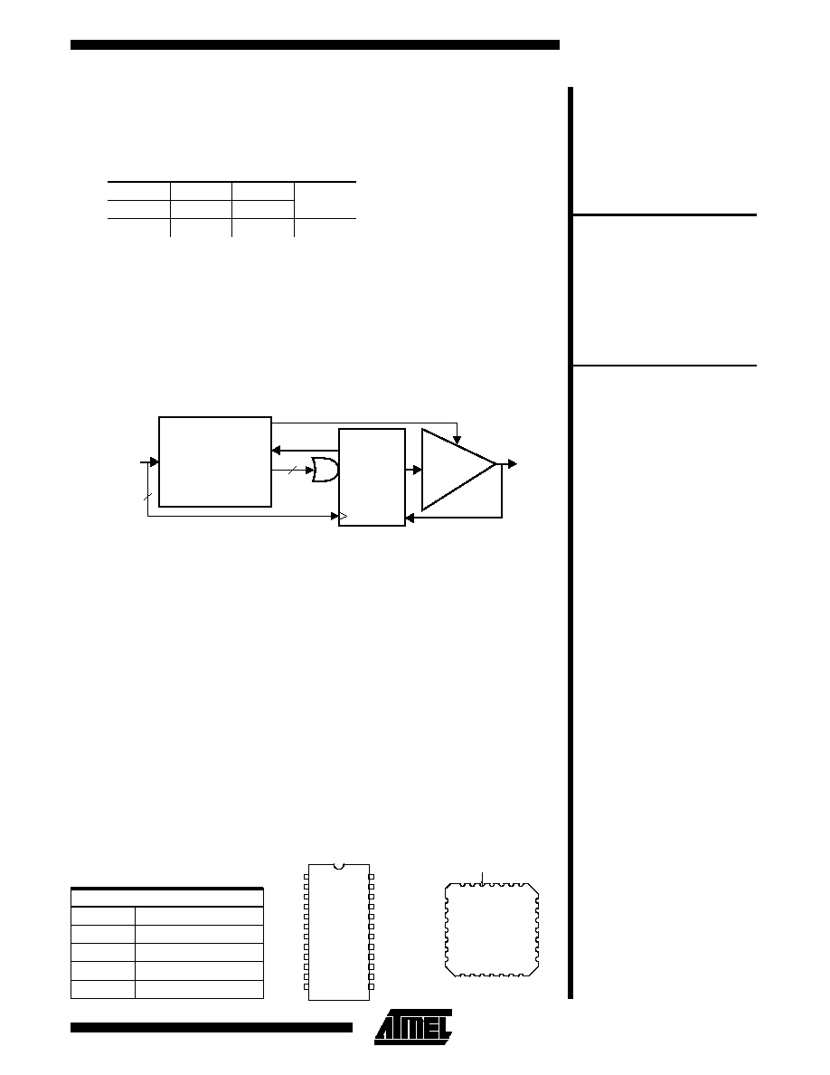
PROGRAMMABLE
INTERCONNECT
AND
COMBINATORIAL
LOGIC ARRAY
LOGIC
OPTION
(UP T0 10
FLIP-FLOPS)
OUTPUT
OPTION
8 TO 16
PRODUCT
TERMS
OE PRODUCT TERMS
10
I/O PINS
12
INPUT PINS
1
Logic Diagram
*
GND IN
I/O
I/O
IN
VCC
*
CLK/IN
I/O
I/O
IN IN
1
15
22
8
GND
15
16
17
18
19
20
21
22
23
24
14
13
12
11
10
9
8
7
6
5
4
3
2
1
IN
Vcc
I/O
I/O
I/O
I/O
I/O
I/O
I/O
I/O
I/O
I/O
IN
CLK/IN
IN
IN
IN
IN
IN
IN
IN
IN
IN
IN
I/O
I/O
I/O
I/O
I/O
I/O
*
IN
IN
IN
IN
IN
IN
*
DIP/SOIC
PLCC
0023C
AT22V10/L
1-97

I/O
OE
Logic
From
Option
Output Options
To
Output
Output
From
Logic Options
I/O
OE
From
Logic
Option
Q
SP
D
AR
Q
CK
To
Output
D.C. and A.C. Operating Conditions
Commercial AT22V10/L
-15, -20, -25
Industrial AT22V10/L
-15, -20, -25
Military AT22V10/L
-15, -20, -25, -30
Operating Temperature (Case)
0
o
C - 70
o
C
-40
o
C - 85
o
C
-55
o
C - 125
o
C
V
CC
Power Supply
5 V
±
10%
5 V
±
10%
5 V
±
10%
Temperature Under Bias.................-55
o
C to +125
o
C
Storage Temperature......................-65
o
C to +150
o
C
Voltage on Any Pin with
Respect to Ground........................ -2.0 V to +7.0 V
(1)
Voltage on Input Pins
with Respect to Ground
During Programming................... -2.0 V to +14.0 V
(1)
Programming Voltage with
Respect to Ground...................... -2.0 V to +14.0 V
(1)
Integrated UV Erase Dose .............. 7258 W
∑
sec/cm
2
*NOTICE: Stresses beyond those listed under "Absolute Maximum
Ratings" may cause permanent damage to the device. This is a
stress rating only and functional operation of the device at these
or any other conditions beyond those indicated in the operational
sections of this specification is not implied. Exposure to absolute
maximum rating conditions for extended periods may affect de-
vice reliability.
Note:
1. Minimum voltage is -0.6 V dc which may undershoot to -2.0 V
for pulses of less than 20 ns. Maximum output pin voltage is
V
CC
+0.75 V dc which may overshoot to +7.0 V for pulses of less
than 20 ns.
Absolute Maximum Ratings*
1-98
AT22V10/L

D.C. Characteristics
Symbol Parameter
Condition
Min
Typ
Max
Units
I
LI
Input Load Current
V
IN
= -0.1 V to V
CC
+1
V
10
µ
A
I
LO
Output Leakage
Current
V
OUT
= -0.1 V to V
CC
+0.1 V
10
µ
A
I
CC
Power Supply
Current
V
CC
= MAX,
V
IN
= GND,
Outputs Open
AT22V10-15,-20
Com.
90
mA
Ind., Mil.
100
mA
AT22V10-25,-35
(2)
55
mA
AT22V10L
(2)
Com.
1.7
12
mA
Ind., Mil.
2.0
15
mA
I
CC2
Clocked Power
Supply Current
V
CC
= MAX,
Outputs Open
AT22V10L
(2)
Com.
2.0
mA/MHz
Ind., Mil.
2.0
mA/MHz
I
OS
(
1
)
Output Short
Circuit Current
V
OUT
= 0.5 V
-120
mA
V
IL
Input Low Voltage
-0.6
0.8
V
V
IH
Input High Voltage
2.0
V
CC
+0.75
V
V
OL
Output Low
Voltage
V
IN
= V
IH
or V
IL
,
V
CC
= MIN
I
OL
= 16 mA
Com.,Ind.
0.5
V
I
OL
= 12 mA
Mil.
0.5
V
I
OL
= 24 mA
Com.
0.8
V
V
OH
Output High
Voltage
V
IN
=V
IH
or V
IL
,
V
CC
=MIN
I
OH
= -100
µ
A
V
CC
-0.3
V
I
OH
= -4.0 mA
2.4
V
2. See I
CC
vs. Frequency curves in the back of this data sheet.
Notes: 1. Not more than one output at a time should be shorted. Du-
ration of short circuit test should not exceed 30 sec.
A.C. Characteristics, Commercial and Industrial
AT22V10-15
AT22V10/L-20
AT22V10/L-25
Symbol Parameter
Min
Typ
Max
Min
Typ
Max
Min
Typ
Max
Units
t
PD
Input or Feedback to
Non-Registered Output
10
15
12
20
15
25
ns
t
EA
Input to Output Enable
10
15
20
15
25
ns
t
ER
Input to Output Disable
10
15
20
15
25
ns
t
CF
Clock to Feedback
0
1
2.5
0
4
8
0
5
10
ns
t
CO
Clock to Output
0
7
10
0
8
12
0
10
15
ns
t
S
Input or Feedback Setup Time
10
8
12
8
15
12
ns
t
H
Hold Time
0
0
0
ns
t
P
Clock Period
12
20
24
ns
t
W
Clock Width
6
10
12
ns
F
MAX
External Feedback 1/(t
S
+t
CO
)
50.0
41.6
33.3
MHz
Internal Feedback 1/(t
S
+ t
CF
)
80.0
50.0
40.0
MHz
No Feedback 1/(t
P
)
83.3
50.0
41.6
MHz
t
AW
Asynchronous Reset Width
15
8
20
9
25
10
ns
t
AR
Asynchronous Reset,
Synchronous Preset,
Recovery Time
15
8
20
12
25
15
ns
t
AP
Asynchronous Reset to
Registered Output Reset
12
20
15
22
18
25
ns
AT22V10/L
1-99

A.C. Characteristics, Military
AT22V10-15
AT22V10/L-20
AT22V10/L-25
AT22V10/L-30
Symbol Parameter
Min
Typ
Max
Min
Typ
Max
Min
Typ
Max
Min
Typ
Max
Units
t
PD
Input or Feedback to
Non-Registered Output
10
15
12
20
15
25
20
30
ns
t
EA
Input to Output Enable
10
15
20
15
25
20
30
ns
t
ER
Input to Output Disable
10
15
20
15
25
20
30
ns
t
CF
Clock to Feedback
0
1
2.5
0
4
8
0
5
10
0
10
15
ns
t
CO
Clock to Output
0
7
10
0
8
15
0
10
15
0
12
20
ns
t
SF
Feedback Setup Time
10
8
12
10
15
12
18
15
ns
t
S
Input Setup Time
10
8
17
14
18
15
20
15
ns
t
H
Hold Time
0
0
0
0
ns
t
P
Clock Period
12
20
24
30
ns
t
W
Clock Width
6
10
12
15
ns
F
MAX
External Feedback 1/(t
S
+t
CO
)
50.0
31.2
30.3
25.0
MHz
Internal Feedback 1/(t
SF
+ t
CF
)
80.0
50.0
40.0
30.0
MHz
No Feedback 1/(t
P
)
83.3
50.0
41.6
33.3
MHz
t
AW
Asynchronous Reset Width
15
8
20
9
25
10
30
15
ns
t
AR
Asynchronous Reset
Recovery Time
15
8
20
12
25
15
30
18
ns
t
AP
Asynchronous Reset to
Registered Output Reset
12
20
15
22
18
25
20
30
ns
OUTPUT
PIN
5.0V
CL= 50pF
R1= 338
R2= 248
Military
AC
MEASUREMENT
LEVEL
AC
DRIVING
LEVELS
0.0V
3.0V
1.5V
tR, tF < 5 ns (10% to 90%)
Input Test Waveforms and
Measurement Levels
Note:
1. Timing measurement reference is 1.5 V. Input AC driving levels are 0.0 V and 3.0 V, unless otherwise specified.
A.C. Waveforms
(1)
OUTPUT
PIN
5.0V
CL= 50pF
R1= 250
R2= 167
Output Test Loads:
Commercial
1-100
AT22V10/L

Functional Logic Diagram AT22V10/L
AT22V10/L
1-101