
1
Features
∑
EE Reprogrammable 2,097,152 x 1-bit Serial Memories Designed to Store
Configuration Programs for Field Programmable Gate Arrays (FPGAs)
∑
In-System Programmable via 2-wire Bus
∑
Simple Interface to SRAM FPGAs
∑
Compatible with Atmel AT6000, AT40K and AT94K Devices, Altera FLEX
Æ
, APEX
TM
Devices, Lucent ORCA
Æ
FPGAs, Xilinx XC3000
TM
, XC4000
TM
, XC5200
TM
, Spartan
Æ
,
Virtex
TM
FPGAs
∑
Cascadable Read Back to Support Additional Configurators or Higher-density Arrays
∑
Low-power CMOS EEPROM Process
∑
Programmable Reset Polarity
∑
Available in 6 mm x 6 mm x 1 mm 8-lead LAP (Pin-compatible with 8-lead SOIC/VOIC
Packages), 20-lead PLCC, 44-lead PLCC and 44-lead TQFP Packages (Pin-compatible
Across Product Family)
∑
Emulation of Atmel's AT24CXXX Serial EEPROMs
∑
Available in 3.3V ± 10% LV and 5V ± 5% C Versions
∑
System-friendly READY Pin
∑
Low-power Standby Mode
∑
Replacement for AT17C/LV020
Description
The AT17C002 and AT17LV002 (high-density AT17 Series) FPGA Configuration
EEPROMs (Configurators) provide an easy-to-use, cost-effective configuration mem-
ory for programming Field Programmable Gate Arrays. The AT17 Series is packaged
in the popular 8-lead LAP, 20-lead PLCC, 44-lead PLCC and the 44-lead TQFP. The
AT17 Series family uses a simple serial-access procedure to configure one or more
FPGA devices. The user can select the polarity of the reset function by programming
four EEPROM bytes. These devices support a write protection mode and a system-
friendly READY pin, which signifies a "good" power level to the FPGA and can be used
to ensure reliable system power-up.
The AT17 Series Configurators can be programmed with industry-standard program-
mers, Atmel's ATDH2200E Programming System and Atmel's ATDH2225 ISP Cable.
FPGA
Configuration
EEPROM
Memory
2-megabit
AT17C002
AT17LV002
Rev. 2281D≠12/01
2
AT17C/LV002
2281D≠12/01
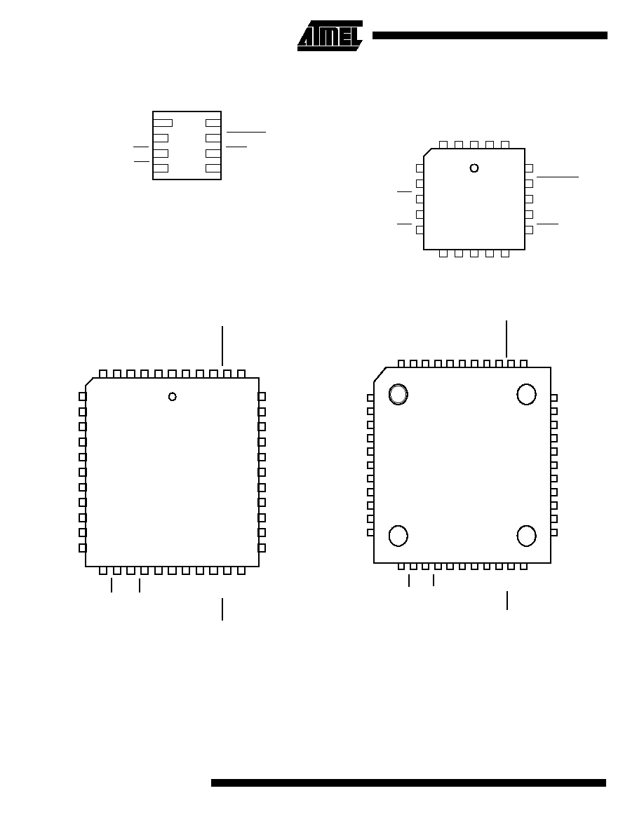
Pin Configuration
8-lead LAP
44-lead PLCC
8
7
6
5
1
2
3
4
DATA
CLK
RESET/OE
CE
VCC
SER_EN
CEO (A2)
GND
7
8
9
10
11
12
13
14
15
16
17
39
38
37
36
35
34
33
32
31
30
29
6
5
4
3
2
1
44
43
42
41
40
18
19
20
21
22
23
24
25
26
27
28
NC
RESET/OE
NC
CE
NC
NC
GND
NC
NC
CEO(A2)
NC
NC
CLK
NC
NC
DATA
NC
VCC
NC
NC
SER_EN
NC
WP1
NC
NC
NC
NC
NC
NC
NC
NC
NC
NC
NC
NC
NC
NC
NC
NC
NC
NC
NC
NC
READY
20-lead PLCC
44-lead TQFP
4
5
6
7
8
18
17
16
15
14
CLK
WP1
RESET/OE
NC
CE
NC
SER_EN
NC
READY
CEO(A2)
3
2
1
20
19
9
10
11
12
13
NC
GND
NC
NC
NC
NC
DATA
NC
VCC
NC
1
2
3
4
5
6
7
8
9
10
11
33
32
31
30
29
28
27
26
25
24
23
44
43
42
41
40
39
38
37
36
35
34
12
13
14
15
16
17
18
19
20
21
22
NC
RESET/OE
NC
CE
NC
NC
GND
NC
NC
CEO(A2)
NC
NC
CLK
NC
NC
DATA
NC
VCC
NC
NC
SER_EN
NC
NC
NC
NC
NC
NC
NC
WP1
NC
NC
NC
NC
NC
NC
NC
NC
NC
NC
NC
NC
NC
NC
READY

3
AT17C/LV002
2281D≠12/01
Block Diagram
Device Description
The control signals for the configuration EEPROM (CE, RESET/OE and CCLK) inter-
face directly with the FPGA device control signals. All FPGA devices can control the
entire configuration process and retrieve data from the configuration EEPROM without
requiring an external intelligent controller.
The configuration EEPROM RESET/OE and CE pins control the tri-state buffer on the
DATA output pin and enable the address counter. When RESET/OE is driven High, the
configuration EEPROM resets its address counter and tri-states its DATA pin. The CE
pin also controls the output of the AT17 Series Configurator. If CE is held High after the
RESET/OE reset pulse, the counter is disabled and the DATA output pin is tri-stated.
When OE is subsequently driven Low, the counter and the DATA output pin are
enabled. When RESET/OE is driven High again, the address counter is reset and the
DATA output pin is tri-stated, regardless of the state of CE.
When the configurator has driven out all of its data and CEO is driven Low, the device
tri-states the DATA pin to avoid contention with other configurators. Upon power-up, the
address counter is automatically reset.
This is the default setting for the device. Since almost all FPGAs use RESET Low and
OE High, this document will describe RESET/OE.
EEPROM
CELL
MATRIX
ROW
DECODER
COLUMN
DECODER
TC
CE
CLK READY
RESET/OE
CEO(A2)
DATA
BIT
COUNTER
OSC
OSC
CONTROL
PROGRAMMING
DATA SHIFT
REGISTER
PROGRAMMING
MODE LOGIC
ROW
ADDRESS
COUNTER
POWER ON
RESET
SER_EN
WP1

4
AT17C/LV002
2281D≠12/01
Note:
1. This pin is not available on the 8-lead packages.
Pin Configurations
8
LAP
Pin
20
PLCC
Pin
44
TQFP
Pin
44
PLCC
Pin
Name
I/O
Description
1
2
40
2
DATA
I/O
Three-state DATA output for configuration. Open-collector bi-directional
pin for programming.
2
4
43
5
CLK
I
Clock input. Used to increment the internal address and bit counter for
reading and programming.
≠
5
7
7
WP1
(1)
I
WRITE PROTECT (1). Used to protect portions of memory during
programming. Disabled by default due to internal pull-down resistor.
This input pin is not used during FPGA loading operations.
3
6
13
19
RESET/OE
I
Output Enable (active High) and RESET (active Low) when SER_EN is
High. A Low level on RESET/OE resets both the address and bit
counters. A High level (with CE Low) enables the data output driver. The
logic polarity of this input is programmable as either RESET/OE or
RESET/OE. For most applications, RESET should be programmed
active Low. This document describes the pin as RESET/OE.
4
8
15
21
CE
I
Chip Enable input (active Low). A Low level (with OE High) allows DCLK
to increment the address counter and enables the data output driver. A
High level on CE disables both the address and bit counters and forces
the device into a low-power standby mode. Note that this pin will not
enable/disable the device in the 2-wire Serial Programming mode
(SER_EN Low).
5
10
18
24
GND
Ground pin. A 0.2 µF decoupling capacitor between
V
CC
and GND is
recommended.
6
14
21
27
CEO
O
Chip Enable Output (active Low). This output goes Low when the
address counter has reached its maximum value. In a daisy chain of
AT17 Series devices, the CEO pin of one device must be connected to
the CE input of the next device in the chain. It will stay Low as long as
CE is low and OE is High. It will then follow CE until OE goes Low;
thereafter, CEO will stay High until the entire EEPROM is read again.
A2
I
Device selection input, A2. This is used to enable (or select) the device
during programming (i.e., when SER_EN is Low). A2 has an internal
pulldown resistor.
≠
15
23
29
READY
(1)
O
Open collector reset state indicator. Driven Low during power-up reset,
released when power-up is complete. (Recommend a 4.7 k
pull-up on
this pin if used).
7
17
35
41
SER_EN
I
Serial enable must be held High during FPGA loading operations.
Bringing SER_EN Low enables the 2-wire Serial Programming Mode.
For non-ISP applications, SER_EN should be tied to V
CC
.
8
20
38
44
V
CC
+3.3V/+5V power supply pin.

5
AT17C/LV002
2281D≠12/01
FPGA Master Serial
Mode Summary
The I/O and logic functions of any SRAM-based FPGA are established by a configura-
tion program. The program is loaded either automatically upon power-up, or on
command, depending on the state of the FPGA mode pins. In Master Mode, the FPGA
automatically loads the configuration program from an external memory. The AT17
Serial Configuration EEPROM has been designed for compatibility with the Master
Serial Mode.
This document discusses the AT40K, AT40KAL and AT94KAL applications, as well as
Xilinx applications.
Control of
Configuration
Most connections between the FPGA device and the AT17 Serial EEPROM are simple
and self-explanatory:
∑
The DATA output of the AT17 Series Configurator drives DIN of the FPGA devices.
∑
The master FPGA CCLK output drives the CLK input of the AT17 Series
Configurator.
∑
The CEO output of any AT17 Series Configurator drives the CE input of the next
Configurator in a cascade chain of EEPROMs.
∑
SER_EN must be connected to V
CC
(except during ISP).
∑
The READY pin is available as an open-collector indicator of the device's reset
status; it is driven Low while the device is in its power-on reset cycle and released
(tri-stated) when the cycle is complete.
Cascading Serial
Configuration
EEPROMs
For multiple FPGAs configured as a daisy-chain, or for FPGAs requiring larger configu-
ration memories, cascaded Configurators provide additional memory.
As the last bit from the first Configurator is read, the clock signal to the Configurator
asserts its CEO output Low and disables its DATA line driver. The second Configurator
recognizes the Low level on its CE input and enables its DATA output.
After configuration is complete, the address counters of all cascaded Configurators are
reset if the RESET/OE on each Configurator is driven to its active (Low) level.
If the address counters are not to be reset upon completion, then the RESET/OE input
can be tied to its inactive (High) level.
AT17 Series Reset
Polarity
The AT17 Series Configurator allows the user to program the reset polarity as either
RESET/OE or RESET/OE. This feature is supported by industry-standard programmer
algorithms.
Programming Mode
The programming mode is entered by bringing SER_EN Low. In this mode the chip can
be programmed by the 2-wire serial bus. The programming is done at V
CC
supply only.
Programming super voltages are generated inside the chip. The AT17C parts are
read/write at 5V nominal. The AT17LV parts are read/write at 3.3V nominal.
Standby Mode
The AT17C/LV002 Series Configurator enters a low-power standby mode whenever CE
is asserted High. In this mode, the Configurator consumes less than 0.5 mA of current at
5V. The output remains in a high-impedance state regardless of the state of the OE
input.