
AT17 Series
1
Pin Configurations
20-pin PLCC
8-Pin DIP
20-Pin SOIC
Features
∑
E
2
Programmable 65,536 x 1, 131,072 x 1, and 262,144 x 1 bit Serial Memories Designed
To Store Configuration Programs For Programmable Gate Arrays
∑
Simple Interface to SRAM FPGAs Requires Only One User I/O Pin
∑
Compatible With AT6000 FPGAs, ATT3000 FPGA, EPF8000 FPGAs, ORCA FPGAs,
XC2000, XC3000, XC4000, XC5000 FPGAs, MPA1000
∑
Cascadable To Support Additional Configurations or Future Higher-density Arrays
(17C128 and 17C256 only)
∑
Low-power CMOS EEPROM Process
∑
Programmable Reset Polarity
∑
Available In the Space-efficient Plastic DIP or Surface-mount
PLCC and SOIC Packages
∑
In-System Programmable Via 2-Wire Bus
∑
Emulation of 24CXX Serial EPROMs
∑
Available in 3.3V
±
10% LV Version
Description
The AT17C65/128/256 and AT17LV65/128/256 (AT17 Series) FPGA Configuration
EEPROMS (Configurator) provide an easy-to-use, cost-effective configuration mem-
ory for Field Programmable Gate Arrays. The AT17 Series is packaged in the 8-pin
DIP and the popular 20-pin PLCC and SOIC. The AT17 Series family uses a simple
serial-access procedure to configure one or more FPGA devices. The AT17 Series
organization supplies enough memory to configure one or multiple smaller FPGAs.
Using a special feature of the AT17 Series, the user can select the polarity of the reset
function by programming a special EEPROM bit.
The AT17 Series can be programmed with industry standard programmers.
0391E-A≠5/97
FPGA
Configuration
E
2
PROM
65K, 128K and 256K
AT17C65
AT17C128
AT17C256
AT17 Series
2
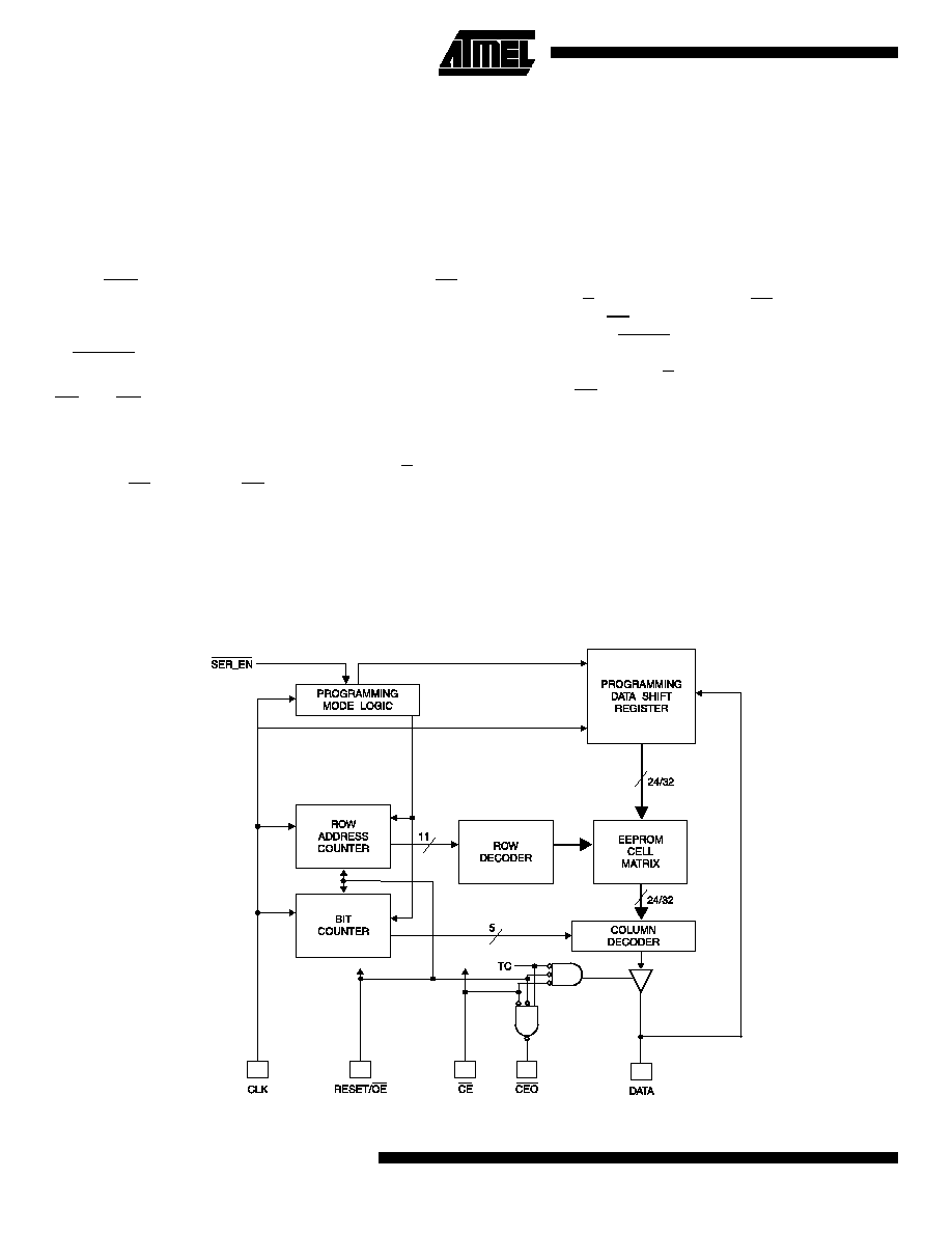
Controlling The AT17 Series Serial EEPROMs
Most connections between the FPGA device and the Serial
EEPROM are simple and self-explanatory.
∑ The DATA output of the AT17 Series drives DIN of the
FPGA devices.
∑ The master FPGA CCLK output drives the CLK input of
the AT17 Series.
∑ The CEO output of any AT17C/LV128/256 drives the CE
input of the next AT17C/LV128/256 in a cascade chain of
PROMs.
∑ SER_EN must be connected to V
CC
.
There are, however, two different ways to use the inputs
CE and OE, as shown in the AC Characteristics wave-
forms.
Condition 1
The simplest connection is to have the FPGA D/P output
drive both CE and RESET/OE in parallel (Figure 1). Due to
its simplicity, however, this method will fail if the FPGA
receives an external reset condition during the configura-
tion cycle. If a system reset is applied to the FPGA, it will
abort the original configuration and then reset itself for a
new configuration, as intended. Of course, the AT17 Series
does not see the external reset signal and will not reset its
internal address counters and, consequently, will remain
out of sync with the FPGA for the remainder of the configu-
ration cycle.
Condition 2
The FPGA D/P output drives only the CE input of the AT17
Series, while its OE input is driven by the inversion of the
input to the FPGA RESET input pin. This connection works
under all normal circumstances, even when the user aborts
a configuration before D/P has gone High. A High level on
the RESET/OE input to the AT17C/LVxxx ≠ during FPGA
reset ≠ clears the Configurator's internal address pointer,
so that the reconfiguration starts at the beginning. The
AT17 Series does not require an inverter since the RESET
polarity is programmable.
Block Diagram
AT17 Series
3
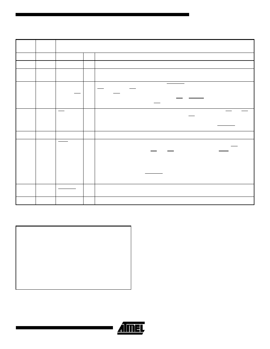
Pin Configurations
PLCC/
SOIC
DIP
Pin
Pin
Name
I/O
Description
2
1
DATA
I/O
Three-state DATA output for reading. Input/Output pin for programming.
4
2
CLK
I
Clock input. Used to increment the internal address and bit counter for reading
and programming.
6
3
RESET/OE
RESET/Output Enable input (when SER_EN is High). A Low level on both the
CE and RESET/OE inputs enables the data output driver. A High level on
RESET/OE resets both the addresss and bit counters. A logic polarity of this
input is programmable as either RESET/OE or RESET/OE. This document
describes the pin as RESET/OE.
8
4
CE
I
Chip Enable input. Used for device selection. A Low level on both CE and OE
enables the data output driver. A High level on CE disables both the address
and bit counters and forces te device into a low power mode. Note this pin will
not enable/disable the device in 2-wire Serial mode (ie; when SER_EN is Low).
10
5
GND
Ground Pin
14
6
CEO
O
Chip Enable Out output. This signal is asserted Low on the clock cycle following
the last bit read from the memory. It will stay Low as long as CE and OE are
both Low. It will then follow CE until OE goes High. Thereafter CEO will stay
High until the entire PROM is read again and senses the status of RESET
polarity.
A2
I
Device selection input, A2. This is used to enable (or select) the device during
programming and when SER_EN is Low (see Programming Guide for more
details).
17
7
SER_EN
I
Serial enable is normally high during FPGA loading operations. Bringing
SER_EN low, enables the 2-wire serial interface for programming.
20
8
V
CC
+3.3V/+5V power supply pin.
Absolute Maximum Ratings*
Operating Temperature......................... -55∞C to +125 ∞C
*NOTICE:
Stresses beyond those listed under "Absolute
Maximum Ratings" may cause permanent dam-
age to the device. This is a stress rating only and
functional operation of the device at these or any
other conditions beyond those indicated in the
operational sections of this specification is not
implied. Exposure to absolute maximum rating
conditions for extended periods may affect device
reliability.
Storage Temperature............................ -65 ∞C to +150∞C
Voltage on Any Pin
with Respect to Ground.................... -0.1V to V
CC +
0.5V
Supply Voltage (Vcc) .............................. -0.5 V to +7.0V
Maximum Soldering Temp. (10 sec. @ 1/16 in.)... 260
∞
C
ESD (R
ZAP
= 1.5K, C
ZAP
= 100pF) ........................2000V

AT17 Series
4
FPGA Master Serial Mode Summary
The I/O and logic functions of the FPGA and their associ-
ated interconnections are established by a configuration
program. The program is loaded either automatically upon
power up, or on command, depending on the state of the
three FPGA mode pins. In Master Mode, the FPGA auto-
matically loads the configuration program from an external
memory. The Serial Configuration EEPROM has been
designed for compatibility with the Master Serial Mode.
Cascading Serial Configuration
EEPROMs
(AT17C/LV128 and AT17C/LV256)
For multiple FPGAs configured as a daisy-chain, or for
future FPGAs requiring larger configuration memories, cas-
caded Configurators provide additional memory (17C/
LV128 and 17C/LV256 only).
After the last bit from the first Configurator is read, the next
clock signal to the Configurator asserts its CEO output Low
and disables its DATA line. The second Configurator recog-
nizes the Low level on its CE input and enables its DATA
output.
Figure 1. Condition 1 Connection
After configuration is complete, the address counters of all
cascaded Configurators are reset if the reset signal drives
the RESET/OE on each Configurator Active.
If the address counters are not to be reset upon comple-
tion, then the RESET/OE inputs can be tied to ground. For
more details, please reference the AT17C Series Program-
ming Guide.
Programming Mode
The programming mode is entered by bringing SER_EN
Low. In this mode the chip can be programmed by the 2-
wire interface. The programming is done at V
CC
supply
only. Programming super voltages are generated inside the
chip. See the Programming Specification for Atmel's Con-
figuration Memories Application Note for further informa-
tion. The AT17C Series parts are read/write at 5V nominal.
The AT17LV parts are read/write at 3.0V nominal.
AT17C/LVXXX Reset Polarity
The AT17C/LVXXX lets the user choose the reset polarity
as either RESET/OE or RESET/OE.
Standby Mode
The AT17C/LVXXX enters a low-power standby mode
whenever CE is asserted High. In this mode, the Configura-
tor consumes less than 1.0 mA of current. The output
remains in a high impedance state regardless of the state
of the OE input.
Operating Conditions
Symbol
Description
AT17CXXX
AT17LVXXX
Units
Min/Max
Min/Max
V
CC
Commercial
Supply voltage relative to GND
-0
∞
C to +70
∞
C
4.75/5.25
3.0/3.6
V
Industrial
Supply voltage relative to GND
-40
∞
C to +85C
∞
4.5/5.5
3.0/3.6
V
Military
Supply voltage relative to GND
-55
∞
C to +125C
4.5/5.5
3.0/3.6
V

AT17 Series
5
DC Characteristics
V
CC
= 5V
±
5% Commercial / 5V
±
10% Ind./Mil.
Symbol
Description
Min
Max
Units
V
IH
High-level input voltage
2.0
V
CC
V
V
IL
Low-level input voltage
0
0.8
V
V
OH
High-level output voltage (I
OH
= -4 mA)
Commercial
3.7
V
V
OL
Low-level output voltage (I
OL
= +4 mA)
0.32
V
V
OH
High-level output voltage (I
OH
= -4 mA)
Industrial
3.6
V
V
OL
Low-level output voltage (I
OL
= +4 mA)
0.37
V
V
OH
High-level output voltage (I
OH
= -4 mA)
Military
3.5
V
V
OL
Low-level output voltage (I
OL
= +4 mA)
0.4
V
I
CCA
Supply current, active mode
10
mA
I
L
Input or output leakage current (V
IN
= V
CC
or GND)
-10
10
µ
A
I
CCS
Supply current, standby mode AT17C256
Commercial
75
µ
A
Industrial/Military
150
µ
A
Supply current, standby mode AT17C128/65
Commercial
1
mA
Industrial/Military
2
mA
DC Characteristics
V
CC
= 3.3V
±
10%
Symbol
Description
Min
Max
Units
V
IH
High-level input voltage
2.0
V
CC
V
V
IL
Low-level input voltage
0
0.8
V
V
OH
High-level output voltage (I
OH
= -2.5 mA)
Commercial
2.4
V
V
OL
Low-level output voltage (I
OL
= +3 mA)
0.4
V
V
OH
High-level output voltage (I
OH
= -2 mA)
Industrial
2.4
V
V
OL
Low-level output voltage (I
OL
= +3 mA)
0.4
V
V
OH
High-level output voltage (I
OH
= -2 mA)
Military
2.4
V
V
OL
Low-level output voltage (I
OL
= +2.5 mA)
0.4
V
I
CCA
Supply current, active mode
5
mA
I
L
Input or output leakage current (V
IN
= V
CC
or GND)
-10
10
µ
A
I
CCS
Supply current, standby mode
Commercial
50
µ
A
Industrial/Military
100
µ
A