1
Features
∑
EE Programmable 65,536 x 1-, 131,072 x 1-, 262,144 x 1-, 524,288 x 1-, 1,048,576 x 1- and
2,097,152 x 1-bit Serial Memories Designed to Store Configuration Programs for Altera
FLEX
Æ
and APEX FPGAs (Device Selection Guide Included)
∑
Available as a 3.3V (±10%) and 5.0V (±5% Commercial, ±10% Industrial) Version
∑
In-System Programmable (ISP) via 2-wire Bus
∑
Simple Interface to SRAM FPGAs
∑
Compatible with Atmel AT6000, AT40K and AT94K Devices, Altera FLEX
Æ
, APEX
TM
Devices, Lucent ORCA
Æ
FPGAs, Xilinx XC3000
TM
, XC4000
TM
, XC5200
TM
, Spartan
Æ
, Virtex
Æ
FPGAs, Motorola MPA1000 FPGAs
∑
Cascadable Read-back to Support Additional Configurations or Higher-density Arrays
∑
Very Low-power CMOS EEPROM Process
∑
Programmable Reset Polarity
∑
Available 8-lead PDIP, 20-lead PLCC and 32-lead TQFP Packages (Pin Compatible
Across Product Family)
∑
Emulation of Atmel's AT24CXXX Serial EEPROMs
∑
Low-power Standby Mode
∑
High-reliability
≠ Endurance: 100,000 Write Cycles
≠ Data Retention: 90 Years for Industrial Parts (at 85
∞C) and 190 Years for
Commercial Parts (at 70
∞C)
Description
The AT17A series FPGA configuration EEPROMs (Configurators) provide an easy-to-
use, cost-effective configuration memory for Field Programmable Gate Arrays. The
AT17A series device is packaged in the 8-lead PDIP
(1)
, 20-lead PLCC and 32-lead
TQFP, see Table 1. The AT17A series configurator uses a simple serial-access proce-
dure to configure one or more FPGA devices. The user can select the polarity of the
reset function by programming four EEPROM bytes.These devices also support a
write-protection mechanism within its programming mode.
Note:
1. The 8-lead LAP, PDIP and SOIC packages for the AT17LV65A/128A/256A do not
have an A label. However, the 8-lead packages are pin compatible with the 8-lead
package of Altera's EEPROMs, refer to the AT17LV65/128/256/512/010/002/040
datasheet available on the Atmel web site for more information.
The AT17A series configurators can be programmed with industry-standard program-
mers, Atmel's ATDH2200E Programming Kit or Atmel's ATDH2225 ISP Cable.
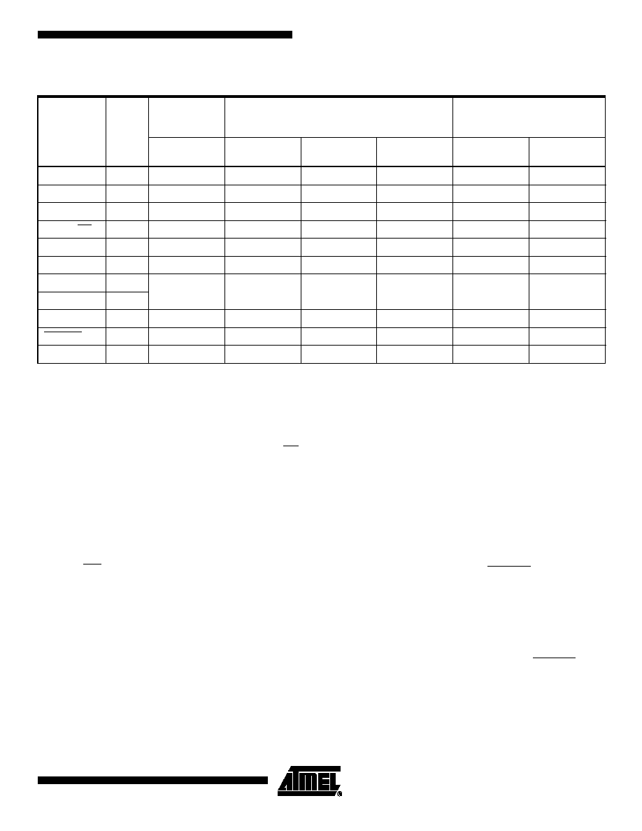
Table 1. AT17A Series Packages
Package
AT17LV65A/
AT17LV128A/
AT17LV256A
AT17LV512A
AT17LV010A
AT17LV002A
8-lead
PDIP
Yes
Yes
Yes
≠
20-lead
PLCC
Yes
Yes
Yes
Yes
32-lead
TQFP
≠
≠
Yes
Yes
FPGA
Configuration
EEPROM
Memory
AT17LV65A
AT17LV128A
AT17LV256A
AT17LV512A
AT17LV010A
AT17LV002A
3.3V and 5V
System Support
Rev. 2322D≠CNFG≠07/02

4
AT17LV65A/128A/256A/512A/002A
2322D≠CNFG≠07/02
Device Description
The control signals for the configuration EEPROM (nCS, RESET/OE and DCLK) inter-
face directly with the FPGA device control signals. All FPGA devices can control the
entire configuration process and retrieve data from the configuration EEPROM without
requiring an external controller.
The configuration EEPROM's RESET/OE and nCS pins control the tri-state buffer on
the DATA output pin and enable the address counter and the oscillator. When
RESET/OE is driven Low, the configuration EEPROM resets its address counter and tri-
states its DATA pin. The nCS pin also controls the output of the AT17A series configura-
tor. If nCS is held High after the RESET/OE pulse, the counter is disabled and the DATA
output pin is tri-stated. When nCS is driven subsequently Low, the counter and the
DATA output pin are enabled. When RESET/OE is driven Low again, the address
counter is reset and the DATA output pin is tri-stated, regardless of the state of the nCS.
When the configurator has driven out all of its data and nCASC is driven Low, the device
tri-states the DATA pin to avoid contention with other configurators. Upon power-up, the
address counter is automatically reset.
This is the default setting for the device. Since almost all FPGAs use RESET Low and
OE High, this document will describe RESET/OE.
5
AT17LV65A/128A/256A/512A/002A
2322D≠CNFG≠07/02
DATA
Three-state DATA output for configuration. Open-collector bi-directional pin for
programming.
DCLK
Clock output or clock input. Rising edges on DCLK increment the internal address
counter and present the next bit of data to the DATA pin. The counter is incremented
only if the RESET/OE input is held High, the nCS input is held Low, and all configuration
data has not been transferred to the target device (otherwise, as the master device, the
DCLK pin drives Low).
WP1
WRITE PROTECT (1). This pin is used to protect portions of memory during program-
ming, and it is disabled by default due to internal pull-down resistor. This input pin is not
u s e d d u r i n g F P G A l o a d i n g o p e r a t i o n s . T h i s p i n i s o n l y a v a i l a b l e o n
AT17LV512A/010A/002A devices.
RESET/OE
Output Enable (active High) and RESET (active Low) when SER_EN is High. A Low
logic level resets the address counter. A High logic level (with nCS Low) enables DATA
and permits the address counter to count. In the mode, if this pin is Low (reset), the
internal oscillator becomes inactive and DCLK drives Low. The logic polarity of this input
is programmable and must be programmed active High (RESET active Low) by the user
during programming for Altera applications.
WP
Write protect (WP) input (when nCS is Low) during programming only (SER_EN Low).
When WP is Low, the entire memory can be written. When WP is enabled (High), the
l owest bl ock of th e m em ory cann ot be wri tten . T his p in is o nly ava ila ble o n
AT17LV65A/128A/256A devices.
Pin Description
Name
I/O
AT17LV65A/
AT17LV128A/
AT17LV256A
AT17LV512A/
AT17LV010A
AT17LV002A
20
PLCC
8
PDIP
20
PLCC
32
TQFP
20
PLCC
32
TQFP
DATA
I/O
2
1
2
31
2
31
DCLK
I
4
2
4
2
4
2
WP1
I
≠
≠
5
4
5
4
RESET/OE
I
8
3
8
7
8
7
nCS
I
9
4
9
10
9
10
GND
10
5
10
12
10
12
nCASC
O
12
6
12
15
12
15
A2
I
READY
O
≠
≠
15
20
15
20
SER_EN
I
18
7
18
23
18
23
V
CC
20
8
20
27
20
27

