1
Features
∑
EE Programmable 262,144 x 1-, 524,288 x 1-, 1,048,576 x 1-, 2,097,152 x 1-, and
4,194,304 x 1-bit Serial Memories Designed to Store Configuration Programs for Field
Programmable Gate Arrays (FPGAs)
∑
Available as a 3.3V (±10%) Commercial and Industrial Version
∑
Simple Interface to SRAM FPGAs
∑
Pin Compatible with Xilinx
Æ
XC17SXXXA and XC17SXXXXL PROMs
∑
Compatible with Xilinx Spartan
Æ
-II, Spartan-IIE and Spartan XL FPGAs in Master Serial
Mode
∑
Very Low-power CMOS EEPROM Process
∑
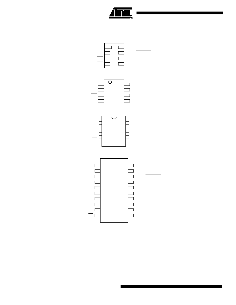
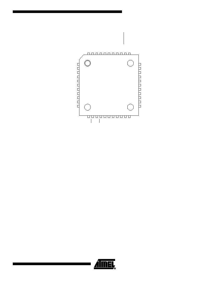
Available in 6 mm x 6 mm x 1 mm 8-lead LAP (Pin-compatible with 8-lead SOIC/VOIC
Packages), 8-lead PDIP, 8-lead SOIC, 20-lead SOIC and 44-lead TQFP Packages for a
Specific Density
∑
Low-power Standby Mode
∑
High-reliability
≠ Endurance: Minimum 10 Write Cycles
≠ Data Retention: 20 Years at 85
∞C
Description
The AT17N series FPGA Configuration EEPROM (Configurators) provide an easy-to-
use, cost-effective configuration memory for Field Programmable Gate Arrays. The
AT17N series device is packaged in the 8-lead LAP, 8-lead PDIP, 8-lead SOIC, 20-lead
SOIC and 44-lead TQFP, see Table 1. The AT17N series Configurators uses a simple
serial-access procedure to configure one or more FPGA devices.
The AT17N series configurators can be programmed with industry-standard program-
mers, Atmel's ATDH2200E Programming Kit or Atmel's ATDH2225 ISP Cable and
factory programming.
Note:
1. The 8-lead LAP package has the same footprint as the 8-lead SOIC. Since an 8-
lead SOIC package is not available for the AT17N512/010/002 devices, it is possi-
ble to use an 8-lead LAP package instead.
Table 1. AT17N Series Packages
Package
AT17N256
AT17N512/
AT17N010
AT17N002
AT17N040
8-lead LAP
≠
Yes
Yes
≠
8-lead PDIP
Yes
Yes
≠
≠
8-lead SOIC
Yes
Use 8-lead LAP
(1)
Use 8-lead LAP
(1)
≠
20-lead SOIC
Yes
Yes
Yes
≠
44-lead TQFP
≠
≠
Yes
Yes
FPGA
Configuration
Memory
AT17N256
AT17N512
AT17N010
AT17N002
AT17N040
3.3V
System Support
Rev. 3020A≠CNFG≠05/03

4
AT17N256/512/010/002/040
3020A≠CNFG≠04/10/03
Block Diagram
Device Description
The control signals for the configuration EEPROM (CE, RESET/OE and CCLK) inter-
face directly with the FPGA device control signals. All FPGA devices can control the
entire configuration process and retrieve data from the configuration EEPROM without
requiring an external intelligent controller.
The configuration EEPROM RESET/OE and CE pins control the tri-state buffer on the
DATA output pin and enable the address counter. When RESET/OE is driven High, the
configuration EEPROM resets its address counter and tri-states its DATA pin. The CE
pin also controls the output of the AT17N series configurator. If CE is held High after the
RESET/OE reset pulse, the counter is disabled and the DATA output pin is tri-stated.
When OE is subsequently driven Low, the counter and the DATA output pin are
enabled. When RESET/OE is driven High again, the address counter is reset and the
DATA output pin is tri-stated, regardless of the state of CE. Upon power-up, the address
counter is automatically reset.
POWER ON
RESET
SER_EN

5
AT17N256/512/010/002/040
3020A≠CNFG≠04/10/03
DATA
Three-state DATA output for configuration. Open-collector bi-directional pin for
programming.
CLK
Clock input. Used to increment the internal address and bit counter for reading and
programming.
RESET/OE
Output Enable (active High) and RESET (active Low) when SER_EN is High. A Low
level on RESET/OE resets both the address and bit counters. A High level (with CE
Low) enables the data output driver. The logic polarity of this input is programmable as
either RESET/OE or RESET/OE. For most applications, RESET should be programmed
active Low. This document describes the pin as RESET/OE.
CE
Chip Enable input (active Low). A Low level (with OE High) allows CLK to increment the
address counter and enables the data output driver. A High level on CE disables both
the address and bit counters and forces the device into a low-power standby mode.
Note that this pin will not enable/disable the device in the Two-Wire Serial Programming
mode (SER_EN Low).
GND
Ground pin. A 0.2 µF decoupling capacitor between V
CC
and GND is recommended.
VCC(SER_EN)
Serial enable must be held High during FPGA loading operations. Bringing SER_EN
Low enables the Two-Wire Serial Programming Mode. For non-ISP applications,
SER_EN should be tied to V
CC
.
V
CC
3.3V (±10%) Commercial and Industrial power supply pin.
NC
NC pins are No Connect pins, which are not internally bonded out to the die.
DC
DC pins are No Connect pins internally connected to the die. It is not recommended to
connect these pins to any external signal.
Pin Description
Name
I/O
AT17N256
AT17N512/
AT17N010
AT17N002
AT17N040
8
DIP/
SOIC
20
SOIC
8
DIP/
LAP
20
SOIC
8
LAP
20
SOIC
44
TQFP
44
TQFP
DATA
I/O
1
1
1
1
1
1
40
40
CLK
I
2
3
2
3
2
3
43
43
RESET/OE
I
3
8
3
8
3
8
13
13
CE
I
4
10
4
10
4
10
15
15
GND
5
11
5
11
5
11
18
18
DC
O
6
13
6
13
6
13
21
21
DC
O
≠
≠
≠
≠
≠
≠
23
23
VCC(SER_EN)
I
7
18
7
18
7
18
35
35
V
CC
8
20
8
20
8
20
38
38