1
Features
∑
Low-Voltage and Standard-Voltage Operation
≠ 2.7 (V
CC
= 2.7V to 5.5V)
≠ 1.8 (V
CC
= 1.8V to 5.5V)
∑
Low-Power Devices (I
SB
= 6
µA @ 5.5V) Available
∑
Internally Organized 4096 x 8, 8192 x 8
∑
2-Wire Serial Interface
∑
Schmitt Trigger, Filtered Inputs for Noise Suppression
∑
Bidirectional Data Transfer Protocol
∑
100 kHz (1.8V) and 400 kHz (2.5V) Clock Rate for AT24C32A
∑
400 kHz (1.8V) Clock Rate for AT24C64A
∑
Write Protect Pin for Hardware Data Protection
∑
32-Byte Page Write Mode (Partial Page Writes Allowed)
∑
Self-Timed Write Cycle (10 ms max)
∑
High Reliability
≠ Endurance: 1 Million Write Cycles
≠ Data Retention: 100 Years
∑
Automotive Grade, Extended Temperature and Lead-Free Devices Available
∑
8-lead JEDEC PDIP, 8-lead JEDEC SOIC, 8-lead MAP and 8-lead TSSOP Packages
Description
The AT24C32A/64A provides 32,768/65,536 bits of serial electrically erasable and
programmable read only memory (EEPROM) organized as 4096/8192 words of 8 bits
each. The device's cascadable feature allows up to 8 devices to share a common 2-
wire bus. The device is optimized for use in many industrial and commercial applica-
tions where low power and low voltage operation are essential. The AT24C32A/64A is
available in space saving 8-lead JEDEC PDIP, 8-lead JEDEC SOIC, 8-lead MAP and
8-lead TSSOP packages and is accessed via a 2-wire serial interface. In addition, the
entire family is available in 2.7V (2.7V to 5.5V) and 1.8V (1.8V to 5.5V) versions.
2-Wire
Serial EEPROM
32K (4096 x 8)
64K (8132 x 8)
AT24C32A
AT24C64A
Rev. 3054H≠SEEPR≠4/03
Pin Configurations
Pin Name
Function
A0 - A2
Address Inputs
SDA
Serial Data
SCL
Serial Clock Input
WP
Write Protect
8-lead PDIP
1
2
3
4
8
7
6
5
A0
A1
A2
GND
VCC
WP
SCL
SDA
8-lead SOIC
1
2
3
4
8
7
6
5
A0
A1
A2
GND
VCC
WP
SCL
SDA
8-lead TSSOP
1
2
3
4
8
7
6
5
A0
A1
A2
GND
VCC
WP
SCL
SDA
8-lead MAP
Bottom View
1
2
3
4
8
7
6
5
A0
A1
A2
GND
VCC
WP
SCL
SDA

2
AT24C32A/64A
3054H≠SEEPR≠4/03
Block Diagram
Absolute Maximum Ratings*
Operating Temperature .................................. -55
∞
C to +125
∞
C
*NOTICE:
Stresses beyond those listed under "Absolute
Maximum Ratings" may cause permanent dam-
age to the device. This is a stress rating only and
functional operation of the device at these or any
other conditions beyond those indicated in the
operational sections of this specification is not
implied. Exposure to absolute maximum rating
conditions for extended periods may affect
device reliability.
Storage Temperature ..................................... -65
∞
C to +150
∞
C
Voltage on Any Pin
with Respect to Ground .....................................-1.0V to +7.0V
Maximum Operating Voltage .......................................... 6.25V
DC Output Current........................................................ 5.0 mA

3
AT24C32A/64A
3054H≠SEEPR≠4/03
Pin Description
SERIAL CLOCK (SCL): The SCL input is used to positive edge clock data into each
EEPROM device and negative edge clock data out of each device.
SERIAL DATA (SDA): The SDA pin is bidirectional for serial data transfer. This pin is
open-drain driven and may be wire-ORed with any number of other open-drain or open
collector devices.
DEVICE/PAGE ADDRESSES (A2, A1, A0): The A2, A1 and A0 pins are device address
inputs that are hard wired or left not connected for hardware compatibility with
AT24C16. When the pins are hardwired, as many as eight 32K/64K devices may be
addressed on a single bus system (device addressing is discussed in detail under the
Device Addressing section). When the pins are not hardwired, the default A
2
, A
1
, and A
0
are zero.
WRITE PROTECT (WP): The write protect input, when tied to GND, allows normal write
operations. When WP is tied high to V
CC
, all write operations to the memory are inhib-
ited. If left unconnected, WP is internally pulled down to GND. Switching WP to V
CC
prior
to a write operation creates a software write protect function.
Memory Organization
AT24C32A/64A, 32K/64K SERIAL EEPROM: The 32K/64K is internally organized as
128/256 pages of 32 bytes each. Random word addressing requires a 12/13-bit data
word address.
4
AT24C32A/64A
3054H≠SEEPR≠4/03
Note:
1. This parameter is characterized and is not 100% tested.
Note:
1. V
IL
min and V
IH
max are reference only and are not tested.
Pin Capacitance
(1)
Applicable over recommended operating range from T
A
= 25
∞
C, f = 1.0 MHz, V
CC
= +1.8V.
Symbol
Test Condition
Max
Units
Conditions
C
I/O
Input/Output Capacitance (SDA)
8
pF
V
I/O
= 0V
C
IN
Input Capacitance (A
0
, A
1
, A
2
, SCL)
6
pF
V
IN
= 0V
DC Characteristics
Applicable over recommended operating range from: T
AI
= -40
∞
C to +85
∞
C, V
CC
= +1.8V to +5.5V, T
AE
= -40
∞
C to +125
∞
C,
V
CC
= +1.8V to +5.5V (unless otherwise noted).
Symbol
Parameter
Test Condition
Min
Typ
Max
Units
V
CC1
Supply Voltage
1.8
5.5
V
V
CC2
Supply Voltage
2.5
5.5
V
V
CC3
Supply Voltage
2.7
5.5
V
V
CC4
Supply Voltage
4.5
5.5
V
I
CC1
Supply Current
V
CC
= 5.0V
READ at 400 kHz
0.4
1.0
mA
I
CC2
Supply Current
V
CC
= 5.0V
WRITE at 400 kHz
2.0
3.0
mA
I
SB1
Standby Current
(1.8V option)
V
CC
= 1.8V
V
IN
= V
CC
or V
SS
1.0
µA
I
SB2
Standby Current
(2.5V option)
V
CC
= 2.5V
V
IN
= V
CC
or V
SS
2.0
µA
I
SB3
Standby Current
(2.7V option)
V
CC
= 2.7V
V
IN
= V
CC
or V
SS
2.0
µA
I
SB4
Standby Current
(5V option)
V
CC
= 4.5 - 5.5V
V
IN
= V
CC
or V
SS
6.0
µA
I
LI
Input Leakage
Current
V
IN
= V
CC
or
V
SS
0.10
3.0
µA
I
LO
Output Leakage
Current
V
OUT
= V
CC
or
V
SS
0.05
3.0
µA
V
IL
Input Low Level
(1)
-0.6
V
CC
x 0.3
V
V
IH
Input High Level
(1)
V
CC
x 0.7
V
CC
+ 0.5
V
V
OL2
Output Low Level
V
CC
= 3.0V
I
OL
= 2.1 mA
0.4
V
V
OL1
Output Low Level
V
CC
= 1.8V
I
OL
= 0.15 mA
0.2
V
5
AT24C32A/64A
3054H≠SEEPR≠4/03
Notes:
1. This parameter is characterized and is not 100% tested (T
A
= 25
∞
C).
2. This parameter is characterized and is not 100% tested.
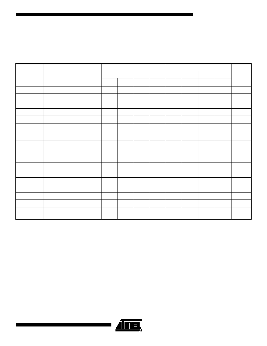
AC Characteristics
Applicable over recommended operating range from T
AI
= -40
∞
C to +85
∞
C, T
AE
= -40
∞
C to +125
∞
C, V
CC
= +1.8V to +5.5V,
CL = 1 TTL Gate and
100 pF (unless otherwise noted).
Symbol
Parameter
AT24C32A
AT24C64A
Units
1.8V
2.5V ≠ 5.0V
1.8V ≠ 3.6V
5.0V
Min
Max
Min
Max
Min
Max
Min
Max
f
SCL
Clock Frequency, SCL
100
400
400
400
kHz
t
LOW
Clock Pulse Width Low
4.7
1.3
1.3
1.2
µs
t
HIGH
Clock Pulse Width High
4.0
0.6
0.6
0.6
µs
t
I
Noise Suppression Time
(1)
100
50
100
50
ns
t
AA
Clock Low to Data Out Valid
0.1
4.5
0.1
0.9
0.2
0.9
0.1
0.9
µs
t
BUF
Time the bus must be free
before a new transmission can
start
(2)
4.7
1.3
1.3
1.2
µs
t
HD.STA
Start Hold Time
4.0
0.6
0.6
0.6
µs
t
SU.STA
Start Set-up Time
4.7
0.6
0.6
0.6
µs
t
HD.DAT
Data In Hold Time
0
0
0
0
µs
t
SU.DAT
Data In Set-up Time
200
100
100
100
ns
t
R
Inputs Rise Time
(2)
1.0
0.3
0.3
0.3
µs
t
F
Inputs Fall Time
(2)
300
300
300
300
ns
t
SU.STO
Stop Set-up Time
4.7
0.6
0.6
0.6
µs
t
DH
Data Out Hold Time
100
50
200
50
ns
t
WR
Write Cycle Time
20
10
20
10
ms
Endurance
(1)
5.0V, 25
∞
C, Page Mode
1M
1M
1M
1M
Write
Cycles