AT27BV010
1 Megabit
(128K x 8)
Unregulated
Battery-Voltage
TM
OTP
CMOS EPROM
Features
∑
Fast Read Access Time - 70 ns
∑
Dual Voltage Range Operation
Unregulated Battery Power Supply Range, 2.7V to 3.6V
or Standard 5V
±
10% Supply Range
∑
Compatible with JEDEC Standard AT27C010
∑
Low Power CMOS Operation
20
µ
A max. (less than 1
µ
A typical) Standby for V
CC
= 3.6V
29 mW max. Active at 5 MHz for V
CC
= 3.6V
∑
JEDEC Standard Packages
32-Lead PLCC
32-Lead TSOP
∑
High Reliability CMOS Technology
2,000V ESD Protection
200 mA Latchup Immunity
∑
Rapid
TM
Programming Algorithm - 100
µ
s/byte (typical)
∑
CMOS and TTL Compatible Inputs and Outputs
JEDEC Standard for LVTTL and LVBO
∑
Integrated Product Identification Code
∑
Commercial and Industrial Temperature Ranges
Description
The AT27BV010 is a high performance, low power, low voltage 1,048,576 bit one-
time programmable read only memory (OTP EPROM) organized as 128K by 8 bits.
It requires only one supply in the range of 2.7V to 3.6V in normal read mode opera-
tion, making it ideal for fast, portable systems using either regulated or unregulated
battery power.
Atmel's innovative design techniques provide fast speeds that rival 5V parts while
keeping the low power consumption of a 3V supply. At V
CC
= 2.7V, any byte can be
accessed in less than 70 ns. With a typical power draw of only 18 mW at 5 MHz and
V
CC
= 3V, the AT27BV010 consumes less than one fifth the power of a standard 5V
(continued)
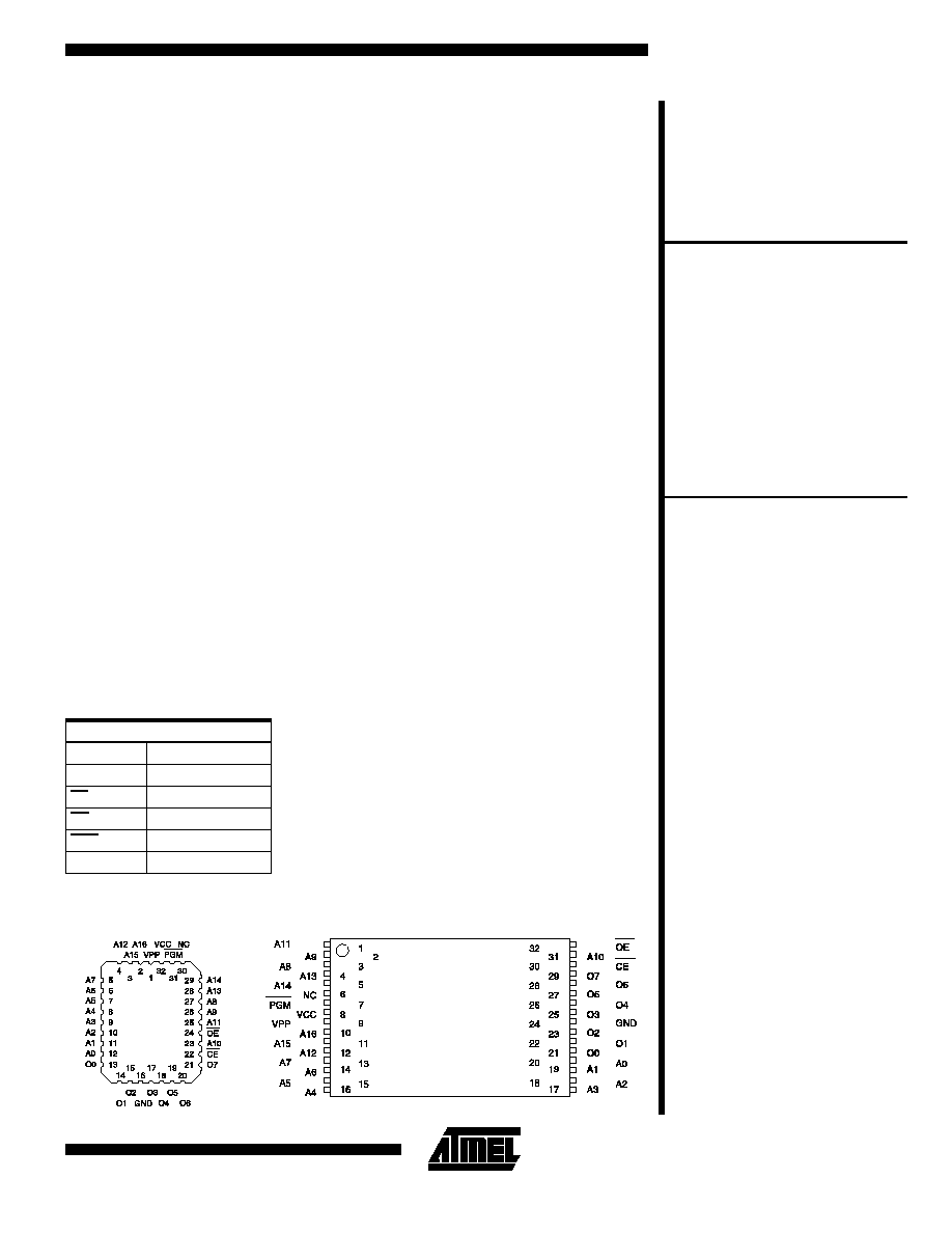
Pin Configurations
Pin Name
Function
A0 - A16
Addresses
O0 - O7
Outputs
CE
Chip Enable
OE
Output Enable
PGM
Program Strobe
NC
No Connect
PLCC Top View
TSOP Top View
Type 1
0344E
AT27BV010
3-23

EPROM. Standby mode supply current is typically less
than 1
µ
A at 3V. The AT27BV010 simplifies system design
and stretches battery lifetime even further by eliminating
the need for power supply regulation.
The AT27BV010 is available in industry standard JEDEC-
approved one-time programmable (OTP) plastic PLCC
and TSOP packages. All devices feature two-line control
(CE, OE) to give designers the flexibility to prevent bus
contention.
The AT27BV010 operating with V
CC
at 3.0V produces TTL
level outputs that are compatible with standard TTL logic
devices operating at V
CC
= 5.0V. At V
CC
= 2.7V, the part
is compatible with JEDEC approved low voltage battery
operation (LVBO) interface specifications. The device is
also capable of standard 5-volt operation making it ideally
suited for dual supply range systems or card products that
are pluggable in both 3-volt and 5-volt hosts.
Atmel's AT27BV010 has additional features to ensure
high quality and efficient production use. The Rapid
TM
Pro-
gramming Algorithm reduces the time required to program
the part and guarantees reliable programming. Program-
ming time is typically only 100
µ
s/byte. The Integrated
Product Identification Code electronically identifies the de-
vice and manufacturer. This feature is used by industry
standard programming equipment to select the proper
programming algorithms and voltages. The AT27BV010
programs exactly the same way as a standard 5V
AT27C010 and uses the same programming equipment.
Description (Continued)
Switching between active and standby conditions via the
Chip Enable pin may produce transient voltage excur-
sions. Unless accommodated by the system design, these
transients may exceed data sheet limits, resulting in de-
vice non-conformance. At a minimum, a 0.1
µ
F high fre-
quency, low inherent inductance, ceramic capacitor
should be utilized for each device. This capacitor should
be connected between the V
CC
and Ground terminals of
the device, as close to the device as possible. Additionally,
to stabilize the supply voltage level on printed circuit
boards with large EPROM arrays, a 4.7
µ
F bulk electrolytic
capacitor should be utilized, again connected between the
V
CC
and Ground terminals. This capacitor should be posi-
tioned as close as possible to the point where the power
supply is connected to the array.
System Considerations
3-24
AT27BV010

Operating Modes
Mode \ Pin
CE
OE
PGM
Ai
V
PP
V
CC
Outputs
Read
(2)
V
IL
V
IL
X
(1)
Ai
X
V
CC
(2)
D
OUT
Output Disable
(2)
X
V
IH
X
X
X
V
CC
(2)
High Z
Standby
(2)
V
IH
X
X
X
X
V
CC
(2)
High Z
Rapid Program
(3)
V
IL
V
IH
V
IL
Ai
V
PP
V
CC
(3)
D
IN
PGM Verify
(3)
V
IL
V
IL
V
IH
Ai
V
PP
V
CC
(3)
D
OUT
PGM Inhibit
(3)
V
IH
X
X
X
V
PP
V
CC
(3)
High Z
Product Identification
(3, 5)
V
IL
V
IL
X
A9 = V
H
(4)
A0 = V
IH
or V
IL
A1 - A16 = V
IL
X
V
CC
(3)
Identification
Code
Notes: 1. X can be V
IL
or V
IH
.
2. Read, output disable, and standby modes require,
2.7V
V
CC
3.6V, or 4.5V
V
CC
5.5V.
3. Refer to Programming Characteristics.
Programming modes require V
CC
=
6.5V
.
4. V
H
= 12.0
±
0.5V.
5. Two identifier bytes may be selected. All Ai inputs are held
low (V
IL
), except A9 which is set to V
H
and A0 which is tog-
gled low (V
IL
) to select the Manufacturer's Identification byte
and high (V
IH
) to select the Device Code byte.
Block Diagram
Temperature Under Bias .................. -40∞C to +85∞C
Storage Temperature...................... -65∞C to +125∞C
Voltage on Any Pin with
Respect to Ground......................... -2.0V to +7.0V
(1)
Voltage on A9 with
Respect to Ground ...................... -2.0V to +14.0V
(1)
V
PP
Supply Voltage with
Respect to Ground....................... -2.0V to +14.0V
(1)
*NOTICE: Stresses beyond those listed under "Absolute Maxi-
mum Ratings" may cause permanent damage to the device.
This is a stress rating only and functional operation of the
device at these or any other conditions beyond those indi-
cated in the operational sections of this specification is not
implied. Exposure to absolute maximum rating conditions
for extended periods may affect device reliability.
Note: 1. Minimum voltage is -0.6V dc which may undershoot
to -2.0V for pulses of less than 20 ns. Maximum out-
put pin voltage is V
CC
+ 0.75V dc which may be ex-
ceeded if certain precautions are observed (consult
application notes) and which may overshoot to
+7.0V for pulses of less than 20 ns.
Absolute Maximum Ratings*
AT27BV010
3-25
DC and Operating Characteristics for Read Operation
Symbol
Parameter
Condition
Min
Max
Units
V
CC
= 2.7V to 3.6V
I
LI
Input Load Current
V
IN
= 0V to V
CC
±
1
µ
A
I
LO
Output Leakage Current
V
OUT
= 0V to V
CC
±
5
µ
A
I
PP1
(
2
)
V
PP
(
1
)
Read/Standby Current
V
PP
= V
CC
10
µ
A
I
SB
V
CC
(
1
)
Standby Current
I
SB1
(CMOS), CE = V
CC
±
0.3V
20
µ
A
I
SB2
(TTL), CE = 2.0 to V
CC
+ 0.5V
100
µ
A
I
CC
V
CC
Active Current
f = 5 MHz, I
OUT
= 0 mA, CE = V
IL
, V
CC
= 3.6V
8
mA
V
IL
Input Low Voltage
V
CC
= 3.0 to 3.6V
-0.6
0.8
V
V
CC
= 2.7 to 3.6V
-0.6
0.2 x V
CC
V
V
IH
Input High Voltage
V
CC
= 3.0 to 3.6V
2.0
V
CC
+ 0.5
V
V
CC
= 2.7 to 3.6V
0.7 x V
CC
V
CC
+ 0.5
V
V
OL
Output Low Voltage
I
OL
= 2.0 mA
0.4
V
I
OL
= 100
µ
A
0.2
V
I
OL
= 20
µ
A
0.1
V
V
OH
Output High Voltage
I
OH
= -2.0
mA
2.4
V
I
OH
= -100
µ
A
V
CC
- 0.2
V
I
OH
= -20
µ
A
V
CC
- 0.1
V
V
CC
= 4.5V to 5.5V
I
LI
Input Load Current
V
IN
= 0V to V
CC
±
1
µ
A
I
LO
Output Leakage Current
V
OUT
= 0V to V
CC
±
5
µ
A
I
PP1
(
2
)
V
PP
(
1
)
Read/Standby Current
V
PP
= V
CC
10
µ
A
I
SB
V
CC
(1)
Standby Current
I
SB1
(CMOS), CE = V
CC
±
0.3V
100
µ
A
I
SB2
(TTL), CE = 2.0 to V
CC
+ 0.5V
1
mA
I
CC
V
CC
Active Current
f = 5 MHz, I
OUT
= 0 mA, CE = V
IL
25
mA
V
IL
Input Low Voltage
-0.6
0.8
V
V
IH
Input High Voltage
2.0
V
CC
+ 0.5
V
V
OL
Output Low Voltage
I
OL
= 2.1 mA
0.4
V
V
OH
Output High Voltage
I
OH
= -400
µ
A
2.4
V
Notes: 1. V
CC
must be applied simultaneously with or before
V
PP
, and removed simultaneously with or after V
PP
.
2. V
PP
may be connected directly to V
CC
, except during pro
gramming. The supply current would then be the sum of I
CC
and I
PP
.
DC and AC Operating Conditions for Read Operation
AT27BV010
-70
-90
-12
-15
Operating Temperature
(Case)
Com.
0∞C - 70∞C
0∞C - 70∞C
0∞C - 70∞C
0∞C - 70∞C
Ind.
-40∞C - 85∞C
-40∞C - 85∞C
-40∞C - 85∞C
-40∞C - 85∞C
V
CC
Power Supply
2.7V to 3.6V
2.7V to 3.6V
2.7V to 3.6V
2.7V to 3.6V
5V
±
10%
5V
±
10%
5V
±
10%
5V
±
10%
= Preliminary Information
3-26
AT27BV010
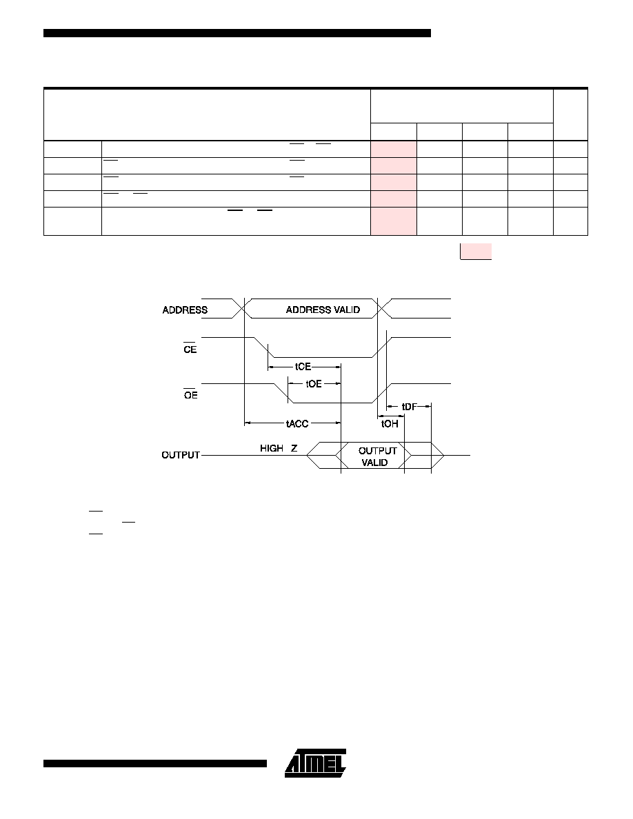
AC Characteristics for Read Operation
(V
CC
= 2.7V to 3.6V and 4.5V to 5.5V)
AT27BV010
-70
-90
-12
-15
Symbol
Parameter
Condition
Min
Max
Min
Max
Min
Max
Min
Max
Units
t
ACC
(3)
Address to Output Delay
CE = OE = V
IL
70
90
120
150
ns
t
CE
(2)
CE to Output Delay
OE = V
IL
70
90
120
150
ns
t
OE
(2, 3)
OE to Output Delay
CE = V
IL
50
50
50
60
ns
t
DF
(4, 5)
OE or CE High to Output Float, whichever occurred first
40
40
40
50
ns
t
OH
Output Hold from Address, CE or OE,
whichever occurred first
0
0
0
0
ns
Notes:
2, 3, 4, 5. - see AC Waveforms for Read Operation.
= Preliminary Information
AC Waveforms for Read Operation
(1)
Notes: 1. Timing measurement references are 0.8V and 2.0V.
Input AC drive levels are 0.45V and 2.4V, unless
otherwise specified.
2. OE may be delayed up to t
CE
- t
OE
after the falling
edge of CE without impact on t
CE
.
3. OE may be delayed up to t
ACC
- t
OE
after the address
is valid without impact on t
ACC
.
4. This parameter is only sampled and is not 100% tested.
5. Output float is defined as the point when data is no longer
driven.
AT27BV010
3-27