AT27BV4096
Note:
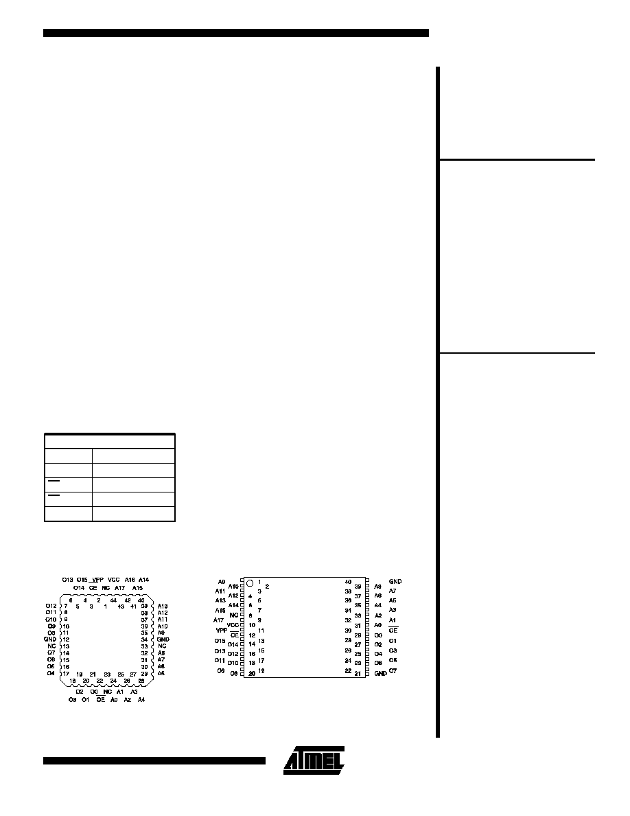
1. PLCC package pins 1 and 23
are DON'T CONNECT.
Description
The AT27BV4096 is a high performance, low power, low voltage 4,194,304 bit one-
time programmable read only memory (OTP EPROM) organized as 256K by 16 bits.
It requires only one supply in the range of 2.7V to 3.6V in normal read mode opera-
tion. The by-16 organization makes this part ideal for portable and handheld 16 and
32 bit microprocessor based systems using either regulated or unregulated battery
power.
(continued)
Pin Configurations
Pin Name
Function
A0 - A17
Addresses
O0 - O15
Outputs
CE
Chip Enable
OE
Output Enable
NC
No Connect
Note: Both GND pins must be
connected.
4 Megabit
(256K x 16)
Unregulated
Battery-Voltage
TM
High Speed
OTP
CMOS EPROM
PLCC Top View
Features
∑
Fast Read Access Time - 120 ns
∑
Dual Voltage Range Operation
Unregulated Battery Power Supply Range, 2.7V to 3.6V
or Standard 5V
±
10% Supply Range
∑
Pin Compatible with JEDEC Standard AT27C4096
∑
Low Power CMOS Operation
20
µ
A max. (less than 1
µ
A typical) Standby for V
CC
= 3.6V
29 mW max. Active at 5 MHz for V
CC
= 3.6V
∑
JEDEC Standard Surface Mount Packages
44-Lead PLCC
40-Lead TSOP (10 x 14mm)
∑
High Reliability CMOS Technology
2,000V ESD Protection
200 mA Latchup Immunity
∑
Rapid
TM
Programming algorithm - 100
µ
s/word (typical)
∑
CMOS and TTL Compatible Inputs and Outputs
JEDEC Standard for LVTTL and LVBO
∑
Integrated Product Identification Code
∑
Commercial and Industrial Temperature Ranges
TSOP Top View
Type 1
0640A
AT27BV4096
3-63

System Considerations
Atmel's innovative design techniques provide fast speeds
that rival 5V parts while keeping the low power consump-
tion of a 3V supply. At V
CC
= 2.7V, any word can be ac-
cessed in less than 120 ns. With a typical power dissipa-
t i on o f on ly 18 m W a t 5 MH z a nd V
CC
= 3 V , t h e
AT27BV4096 consumes less than one fifth the power of a
standard 5V EPROM.
Standby mode supply current is typically less than 1
µ
A at
3V. The AT27BV4096 simplifies system design and
stretches battery lifetime even further by eliminating the
need for power supply regulation.
The AT27BV4096 is available in industry standard
JEDEC-approved one-time programmable (OTP) plastic
PLCC and TSOP packages. All devices feature two-line
control (CE, OE) to give designers the flexibility to prevent
bus contention.
The AT27BV4096 operating with V
CC
at 3.0V produces
TTL level outputs that are compatible with standard TTL
logic devices operating at V
CC
= 5.0V. At V
CC
= 2.7V, the
part is compatible with JEDEC approved low voltage bat-
tery operation (LVBO) interface specifications. The device
is also capable of standard 5-volt operation making it ide-
ally suited for dual supply range systems or card products
that are pluggable in both 3-volt and 5-volt hosts.
Atmel's AT27BV4096 has additional features to ensure
high quality and efficient production use. The Rapid
TM
Pro-
gramming Algorithm reduces the time required to program
the part and guarantees reliable programming. Program-
ming time is typically only 100
µ
s/word. The Integrated
Product Identification Code electronically identifies the de-
vice and manufacturer. This feature is used by industry
standard programming equipment to select the proper
programming algorithms and voltages. The AT27BV4096
programs exactly the same way as a standard 5V
AT27C4096 and uses the same programming equipment.
Description (Continued)
Switching between active and standby conditions via the
Chip Enable pin may produce transient voltage excur-
sions. Unless accommodated by the system design, these
transients may exceed data sheet limits, resulting in de-
vice non-conformance. At a minimum, a 0.1
µ
F high fre-
quency, low inherent inductance, ceramic capacitor
should be utilized for each device. This capacitor should
be connected between the V
CC
and Ground terminals of
the device, as close to the device as possible. Additionally,
to stabilize the supply voltage level on printed circuit
boards with large EPROM arrays, a 4.7
µ
F bulk electrolytic
capacitor should be utilized, again connected between the
V
CC
and Ground terminals. This capacitor should be posi-
tioned as close as possible to the point where the power
supply is connected to the array.
3-64
AT27BV4096
Operating Modes
Mode \ Pin
CE
OE
Ai
V
PP
V
CC
Outputs
Read
(2)
V
IL
V
IL
Ai
X
(1)
V
CC
(2)
D
OUT
Output Disable
(2)
X
V
IH
X
X
V
CC
(2)
High Z
Standby
(2)
V
IH
X
X
X
(5)
V
CC
(2)
High Z
Rapid Program
(3)
V
IL
V
IH
Ai
V
PP
V
CC
(3)
D
IN
PGM Verify
(3)
V
IH
V
IL
Ai
V
PP
V
CC
(3)
D
OUT
PGM Inhibit
(3)
V
IH
V
IH
X
V
PP
V
CC
(3)
High Z
Product Identification
(3, 5)
V
IL
V
IL
A9 = V
H
(4)
A0 = V
IH
or V
IL
A1 - A17 = V
IL
V
CC
V
CC
(3)
Identification
Code
Notes: 1. X can be V
IL
or V
IH
.
2. Read, output disable, and standby modes require,
2.7V
V
CC
3.6V, or 4.5V
V
CC
5.5V.
3. Refer to Programming Characteristics. Programming
modes require V
CC
=
6.5V.
4. V
H
= 12.0
±
0.5V.
5. Two identifier words may be selected. All Ai inputs
are held low (V
IL
), except A9 which is set to V
H
and A0
which is toggled low (V
IL
) to select the Manufacturer's Identi-
fication word and high (V
IH
) to select the Device Code word.
Temperature Under Bias ................ -55
∞
C to +125
∞
C
Storage Temperature...................... -65
∞
C to +150
∞
C
Voltage on Any Pin with
Respect to Ground......................... -2.0V to +7.0V
(1)
Voltage on A9 with
Respect to Ground ...................... -2.0V to +14.0V
(1)
V
PP
Supply Voltage with
Respect to Ground....................... -2.0V to +14.0V
(1)
*NOTICE: Stresses beyond those listed under "Absolute Maxi-
mum Ratings" may cause permanent damage to the device.
This is a stress rating only and functional operation of the
device at these or any other conditions beyond those indi-
cated in the operational sections of this specification is not
implied. Exposure to absolute maximum rating conditions
for extended periods may affect device reliability.
Note: 1. Minimum voltage is -0.6V dc which may undershoot to
-2.0V for pulses of less than 20 ns. Maximum output
pin voltage is V
CC
+ 0.75V dc which may overshoot
to +7.0V for pulses of less than 20 ns.
Absolute Maximum Ratings*
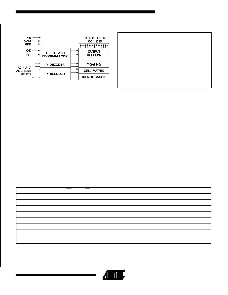
Block Diagram
AT27BV4096
3-65

DC and AC Operating Conditions for Read Operation
AT27BV4096
-12
-15
Operating
Temperature (Case)
Com.
0
∞
C - 70
∞
C
0
∞
C - 70
∞
C
Ind.
-40
∞
C - 85
∞
C
-40
∞
C - 85
∞
C
V
CC
Power Supply
2.7V - 3.6V
2.7V - 3.6V
5V
±
10%
5V
±
10%
DC and Operating Characteristics for Read Operation
Symbol
Parameter
Condition
Min
Max
Units
V
CC
= 2.7V to 3.6V
I
LI
Input Load Current
V
IN
= 0V to V
CC
±
1
µ
A
I
LO
Output Leakage Current
V
OUT
= 0V to V
CC
±
5
µ
A
I
PP1
(
2
)
V
PP
(
1
)
Read/Standby Current
V
PP
= V
CC
10
µ
A
I
SB
V
CC
(
1
)
Standby Current
I
SB1
(CMOS), CE = V
CC
±
0.3V
20
µ
A
I
SB2
(TTL), CE = 2.0 to V
CC
+ 0.5V
100
µ
A
I
CC
V
CC
Active Current
f = 5 MHz, I
OUT
= 0 mA, CE = V
IL
, V
CC
= 3.6V
8
mA
V
IL
Input Low Voltage
V
CC
= 3.0 to 3.6V
-0.6
0.8
V
V
CC
= 2.7 to 3.6V
-0.6
0.2 x V
CC
V
V
IH
Input High Voltage
V
CC
= 3.0 to 3.6V
2.0
V
CC
+ 0.5
V
V
CC
= 2.7 to 3.6V
0.7 x V
CC
V
CC
+ 0.5
V
V
OL
Output Low Voltage
I
OL
= 2.0 mA
0.4
V
I
OL
= 100
µ
A
0.2
V
I
OL
= 20
µ
A
0.1
V
V
OH
Output High Voltage
I
OH
= -2.0
mA
2.4
V
I
OH
= -100
µ
A
V
CC
- 0.2
V
I
OH
= -20
µ
A
V
CC
- 0.1
V
V
CC
= 4.5V to 5.5V
I
LI
Input Load Current
V
IN
= 0V to V
CC
±
1
µ
A
I
LO
Output Leakage Current
V
OUT
= 0V to V
CC
±
5
µ
A
I
PP1
(
2
)
V
PP
(
1
)
Read/Standby Current
V
PP
= V
CC
10
µ
A
I
SB
V
CC
(1)
Standby Current
I
SB1
(CMOS), CE = V
CC
±
0.3V
100
µ
A
I
SB2
(TTL), CE = 2.0 to V
CC
+ 0.5V
1
mA
I
CC
V
CC
Active Current
f = 5 MHz, I
OUT
= 0 mA, CE = V
IL
40
mA
V
IL
Input Low Voltage
-0.6
0.8
V
V
IH
Input High Voltage
2.0
V
CC
+ 0.5
V
V
OL
Output Low Voltage
I
OL
= 2.1 mA
0.4
V
V
OH
Output High Voltage
I
OH
= -400
µ
A
2.4
V
Notes: 1. V
CC
must be applied simultaneously with or before
V
PP
, and removed simultaneously with or after
V
PP
.
2. V
PP
may be connected directly to V
CC
, except during pro-
gramming. The supply current would then be the sum of I
CC
and I
PP
.
= Preliminary Information
3-66
AT27BV4096

AC Characteristics for Read Operation
(V
CC
= 2.7V to 3.6V and 4.5V to 5.5V)
AT27BV4096
-12
-15
Symbol
Parameter
Condition
Min
Max
Min
Max
Units
t
ACC
(3)
Address to
Output Delay
CE = OE
=
V
IL
120
150
ns
t
CE
(2)
CE to Output Delay
OE = V
IL
120
150
ns
t
OE
(2, 3)
OE to Output Delay
CE = V
IL
35
50
ns
t
DF
(4, 5)
OE or CE High to Output Float, whichever occurred first
30
40
ns
t
OH
Output Hold from Address, CE or OE,
whichever occurred first
0
0
ns
Notes: 2, 3, 4, 5. - see AC Waveforms for Read Operation.
= Preliminary Information
AC Waveforms for Read Operation
(1)
Notes: 1. Timing measurement references are 0.8V and 2.0V.
Input AC drive levels are 0.45V and 2.4V, unless oth-
erwise specified.
2. OE may be delayed up to t
CE
- t
OE
after the falling
edge of CE without impact on t
CE
.
3. OE may be delayed up to t
ACC
- t
OE
after the address
is valid without impact on t
ACC
.
4. This parameter is only sampled and is not 100% tested.
5. Output float is defined as the point when data is no longer
driven.
6. When reading a 27BV4096, a 0.1
µ
F capacitor is required
across V
CC
and ground to supress spurious voltage tran-
sients.
AT27BV4096
3-67