AT89LS53
4-249
Features
∑
Compatible with MCS-51
TM
Products
∑
12K Bytes of In-System Reprogrammable Downloadable Flash Memory
- SPI Serial Interface for Program Downloading
- Endurance: 1,000 Write/Erase Cycles
∑
2.7V to 6V Operating Range
∑
Fully Static Operation: 0 Hz to 12 MHz
∑
Three-Level Program Memory Lock
∑
256 x 8 bit Internal RAM
∑
32 Programmable I/O Lines
∑
Three 16-bit Timer/Counters
∑
Nine Interrupt Sources
∑
Programmable UART Serial Channel
∑
SPI Serial Interface
∑
Low Power Idle and Power Down Modes
∑
Interrupt Recovery From Power Down
∑
Programmable Watchdog Timer
∑
Dual Data Pointer
∑
Power Off Flag
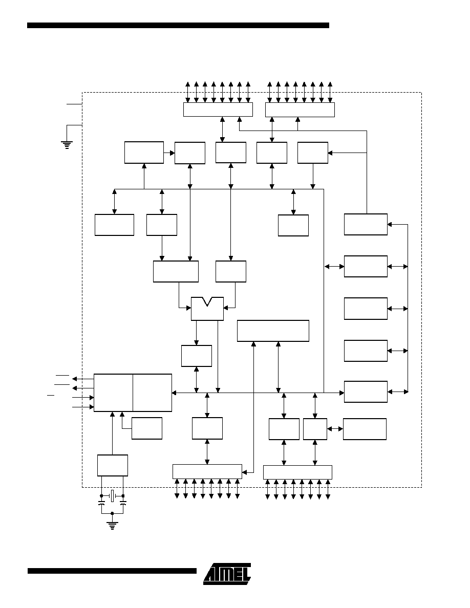
Description
The AT89LS53 is a low-power, wide-voltage range, high-performance CMOS 8-bit
microcomputer with 12K bytes of downloadable Flash programmable and erasable
read only memory. The device is manufactured using Atmel's high density nonvolatile
memory technology and is compatible with the industry standard 80C51 instruction
set and pinout. The on-chip downloadable Flash allows the program memory to be
reprogrammed in-system through an SPI serial interface or by a conventional nonvol-
atile memory programmer. By combining a versatile 8-bit CPU with downloadable
Flash on a monolithic chip, the Atmel AT89LS53 is a powerful microcomputer which
provides a highly flexible and cost effective solution to many embedded control appli-
cations.
The AT89LS53 provides the following standard features: 12K bytes of downloadable
Flash, 256 bytes of RAM, 32 I/O lines, programmable watchdog timer, two Data Point-
ers, three 16-bit timer/counters, a six-vector two-level interrupt architecture, a full
duplex serial port, on-chip oscillator, and clock circuitry. In addition, the AT89LS53 is
designed with static logic for operation down to zero frequency and supports two soft-
ware selectable power saving modes. The Idle Mode stops the CPU while allowing
the RAM, timer/counters, serial port, and interrupt system to continue functioning. The
Power Down Mode saves the RAM contents but freezes the oscillator, disabling all
other chip functions until the next interrupt or hardware reset.
The downloadable Flash can be changed a single byte at a time and is accessible
through the SPI serial interface. Holding RESET active forces the SPI bus into a serial
programming interface and allows the program memory to be written to or read from
unless Lock Bit 2 has been activated.
0851B-B≠12/97
8-Bit
Microcontroller
with 12K Bytes
Flash
AT89LS53
AT89LS53
4-250
Pin Description
V
CC
Supply voltage.
GND
Ground.
Port 0
Port 0 is an 8-bit open drain bidirectional I/O port. As an
output port, each pin can sink eight TTL inputs. When 1s
are written to port 0 pins, the pins can be used as high-
impedance inputs.
Port 0 can also be configured to be the multiplexed low-
order address/data bus during accesses to external pro-
gram and data memory. In this mode, P0 has internal pul-
lups.
Port 0 also receives the code bytes during Flash program-
ming and outputs the code bytes during program verifica-
tion. External pullups are required during program verifica-
tion.
Port 1
Port 1 is an 8-bit bidirectional I/O port with internal pullups.
The Port 1 output buffers can sink/source four TTL inputs.
When 1s are written to Port 1 pins, they are pulled high by
the internal pullups and can be used as inputs. As inputs,
Port 1 pins that are externally being pulled low will source
current (I
IL
) because of the internal pullups.
Some Port 1 pins provide additional functions. P1.0 and
P1.1 can be configured to be the timer/counter 2 external
count input (P1.0/T2) and the timer/counter 2 trigger input
(P1.1/T2EX), respectively.
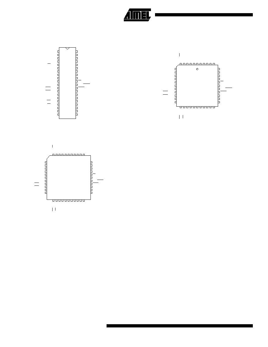
Pin Configurations
PDIP
1
2
3
4
5
6
7
8
9
10
11
12
13
14
15
16
17
18
19
20
40
39
38
37
36
35
34
33
32
31
30
29
28
27
26
25
24
23
22
21
(T2) P1.0
(T2 EX) P1.1
P1.2
P1.3
(SS) P1.4
(MOSI) P1.5
(MISO) P1.6
(SCK) P1.7
RST
(RXD) P3.0
(TXD) P3.1
(INT0) P3.2
(INT1) P3.3
(T0) P3.4
(T1) P3.5
(WR) P3.6
(RD) P3.7
XTAL2
XTAL1
GND
VCC
P0.0 (AD0)
P0.1 (AD1)
P0.2 (AD2)
P0.3 (AD3)
P0.4 (AD4)
P0.5 (AD5)
P0.6 (AD6)
P0.7 (AD7)
EA/VPP
ALE/PROG
PSEN
P2.7 (A15)
P2.6 (A14)
P2.5 (A13)
P2.4 (A12)
P2.3 (A11)
P2.2 (A10)
P2.1 (A9)
P2.0 (A8)
PLCC
7
8
9
10
11
12
13
14
15
16
17
39
38
37
36
35
34
33
32
31
30
29
(MOSI) P1.5
(MISO) P1.6
(SCK) P1.7
RST
(RXD) P3.0
NC
(TXD) P3.1
(INT0) P3.2
(INT1) P3.3
(T0) P3.4
(T1) P3.5
P0.4 (AD4)
P0.5 (AD5)
P0.6 (AD6)
P0.7 (AD7)
EA/VPP
NC
ALE/PROG
PSEN
P2.7 (A15)
P2.6 (A14)
P2.5 (A13)
6
5
4
3
2
1
44
43
42
41
40
18
19
20
21
22
23
24
25
26
27
28
(WR) P3.6
(RD) P3.7
XTAL2
XTAL1
GND
NC
(A8) P2.0
(A9) P2.1
(A10) P2.2
(A11) P2.3
(A12) P2.4
P1.4 (SS)
P1.3
P1.2
P1.1 (T2 EX)
P1.0 (T2)
NC
VCC
P0.0 (AD0)
P0.1 (AD1)
P0.2 (AD2)
P0.3 (AD3)
TQFP
1
2
3
4
5
6
7
8
9
10
11
33
32
31
30
29
28
27
26
25
24
23
44
43
42
41
40
39
38
37
36
35
34
12
13
14
15
16
17
18
19
20
21
22
(MOSI) P1.5
(MISO) P1.6
(SCK) P1.7
RST
(RXD) P3.0
NC
(TXD) P3.1
(INT0) P3.2
(INT1) P3.3
(T0) P3.4
(T1) P3.5
P0.4 (AD4)
P0.5 (AD5)
P0.6 (AD6)
P0.7 (AD7)
EA/VPP
NC
ALE/PROG
PSEN
P2.7 (A15)
P2.6 (A14)
P2.5 (A13)
P1.4 (SS)
P1.3
P1.2
P1.1 (T2 EX)
P1.0 (T2)
NC
VCC
P0.0 (AD0)
P0.1 (AD1)
P0.2 (AD2)
P0.3 (AD3)
(WR) P3.6
(RD) P3.7
XTAL2
XTAL1
GND
GND
(A8) P2.0
(A9) P2.1
(A10) P2.2
(A11) P2.3
(A12) P2.4

AT89LS53
4-252
Pin Description
Furthermore, P1.4, P1.5, P1.6, and P1.7 can be configured
as the SPI slave port select, data input/output and shift
clock input/output pins as shown in the following table.
Port 1 also receives the low-order address bytes during
Flash programming and verification.
Port 2
Port 2 is an 8-bit bidirectional I/O port with internal pullups.
The Port 2 output buffers can sink/source four TTL inputs.
When 1s are written to Port 2 pins, they are pulled high by
the internal pullups and can be used as inputs. As inputs,
Port 2 pins that are externally being pulled low will source
current (I
IL
) because of the internal pullups.
Port 2 emits the high-order address byte during fetches
from external program memory and during accesses to
external data memory that use 16-bit addresses (MOVX @
DPTR). In this application, Port 2 uses strong internal pul-
lups when emitting 1s. During accesses to external data
memory that use 8-bit addresses (MOVX @ RI), Port 2
emits the contents of the P2 Special Function Register.
Port 2 also receives the high-order address bits and some
control signals during Flash programming and verification.
Port 3
Port 3 is an 8 bit bidirectional I/O port with internal pullups.
The Port 3 output buffers can sink/source four TTL inputs.
When 1s are written to Port 3 pins, they are pulled high by
the internal pullups and can be used as inputs. As inputs,
Port 3 pins that are externally being pulled low will source
current (I
IL
) because of the pullups.
Port 3 also serves the functions of various special features
of the AT89LS53, as shown in the following table.
Port 3 also receives some control signals for Flash pro-
gramming and verification.
RST
Reset input. A high on this pin for two machine cycles while
the oscillator is running resets the device.
ALE/PROG
Address Latch Enable is an output pulse for latching the
low byte of the address during accesses to external mem-
ory. This pin is also the program pulse input (PROG) during
Flash programming.
In normal operation, ALE is emitted at a constant rate of 1/
6 the oscillator frequency and may be used for external tim-
ing or clocking purposes. Note, however, that one ALE
pulse is skipped during each access to external data mem-
ory.
If desired, ALE operation can be disabled by setting bit 0 of
SFR location 8EH. With the bit set, ALE is active only dur-
ing a MOVX or MOVC instruction. Otherwise, the pin is
weakly pulled high. Setting the ALE-disable bit has no
effect if the microcontroller is in external execution mode.
PSEN
Program Store Enable is the read strobe to external pro-
gram memory.
When the AT89LS53 is executing code from external pro-
gram memory, PSEN is activated twice each machine
cycle, except that two PSEN activations are skipped during
each access to external data memory.
EA/V
PP
External Access Enable. EA must be strapped to GND in
order to enable the device to fetch code from external pro-
gram memory locations starting at 0000H up to FFFFH.
Note, however, that if lock bit 1 is programmed, EA will be
internally latched on reset.
EA should be strapped to V
CC
for internal program execu-
tions. This pin also receives the 12-volt programming
enable voltage (V
PP
) during Flash programming when 12-
volt programming is selected.
Port Pin
Alternate Functions
P1.0
T2 (external count input to Timer/Counter
2), clock-out
P1.1
T2EX (Timer/Counter 2 capture/reload
trigger and direction control)
P1.4
SS (Slave port select input)
P1.5
MOSI (Master data output, slave data input
pin for SPI channel)
P1.6
MISO (Master data input, slave data output
pin for SPI channel)
P1.7
SCK (Master clock output, slave clock input
pin for SPI channel)
Port Pin
Alternate Functions
P3.0
RXD (serial input port)
P3.1
TXD (serial output port)
P3.2
INT0 (external interrupt 0)
P3.3
INT1 (external interrupt 1)
P3.4
T0 (timer 0 external input)
P3.5
T1 (timer 1 external input)
P3.6
WR (external data memory write strobe)
P3.7
RD (external data memory read strobe)