
1
Features
∑
Incorporates the ARM7TDMI
TM
ARM Thumb processor
≠ High-performance 32-bit RISC architecture
≠ High-density 16-bit instruction set
≠ Leader in MIPS/Watt
≠ Embedded ICE In Circuit Emulation
∑
4K bytes internal RAM
∑
Fully programmable External Bus Interface (EBI)
≠ Maximum external address space of 64M bytes
≠ Up to eight chip selects
≠ Software programmable 8/16-bit external databus
∑
Eight-level priority, individually maskable, vectored interrupt controller
≠ Four External interrupts, including a high priority low latency interrupt request
∑
32 Programmable I/O lines
∑
Three-channel 16-bit timer/counter
≠ Three external clock inputs
≠ Two multi-purpose I/O pins per channel
∑
Two USARTs
≠ Two dedicated Peripheral Data Controller (PDC) channels per USART
∑
Programmable watchdog timer
∑
Low-power idle and power-down modes
∑
Fully static operation: 0 Hz to 33 MHz
∑
2.7V to 3.6V operating range
∑
Available in a 100-lead TQFP package
Description
The AT91M40400 is a member of the Atmel AT91 16/32-bit Microcontroller family
which is based on the ARM7TDMI embedded processor. This processor has a high-
performance 32-bit RISC architecture with a high-density 16-bit instruction set and
very low power consumption. In addition, a large number of internally banked registers
result in very fast exception handling, making the device ideal for real-time control
applications. The AT91 ARM-based MCU family also features Atmel's high-density,
nonvolatile memory technology. The on-chip Flash program memory is in-system pro-
grammable.
The AT91M40400 has a direct connection to off-chip memory, including Flash,
through the External Bus Interface.
The device is manufactured using Atmel's high-density CMOS technology. By com-
bining the ARM7TDMI microcontroller core with an on-chip RAM and a wide range of
peripheral functions on a monolithic chip, the Atmel AT91M40400 is a powerful micro-
controller that provides a flexible, cost-effective solution to many compute-intensive
embedded control applications.
Rev. 0768BS≠08/98
16/32-Bit
Microcontroller
AT91M40400
Summary
Full datasheet (lit# 0768B)
also available by e-mailing
literature@atmel.com
AT91M40400
2
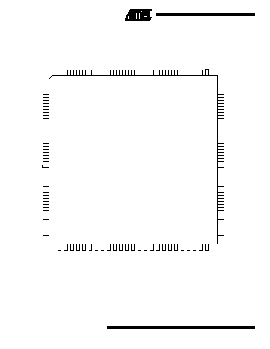
Pin Configuration
Figure 1. AT91M40400 Pinout (Top View)
P21/TXD1/NTRI
P20/SCK1
P19
P18
P17
P16
P15/RXD0
P14/TXD0
P13/SCK0
P12/FIQ
GND
P11/IRQ2
P10/IRQ1
VDD
VDD
P9/IRQ0
P8/TIOB2
P7/TIOA2
P6/TCLK2
P5/TIOB1
P4/TIOA1
P3/TCLK1
GND
GND
P2/TIOB0
P1/TIOA0
P0/TCLK0
D15
D14
D13
D12
VDD
D11
D10
D9
D8
D7
D6
D5
GND
D4
D3
D2
D1
D0
P31/A23/CS4
P30/A22/CS5
VDD
VDD
P29/A21/CS6
P22/RXD1
NWR1/NUB
GND
NRST
NWDOVF
VDD
MCKI
P23
P24/BMS
P25/MCKO
GND
GND
TMS
TDI
TDO
TCK
NRD/NOE
NWR0/NWE
VDD
VDD
NWAIT
NCS0
NCS1
P26/NCS2
P27/NCS3
A0/NLB
A1
A2
A2
A3
A4
A5
A6
A7
VDD
A8
A9
A10
A11
A12
A13
A14
GND
GND
A15
A16
A17
A18
A19
P28/A20/CS7
GND
1
25
AT91M40400
100-Lead TQFP
2
3
4
5
6
7
8
9
10
11
12
13
14
15
1
16
17
18
19
20
21
22
23
24
26
50
27
28
29
30
31
32
33
34
35
36
37
38
39
40
41
42
43
44
45
46
47
48
49
75
51
74
73
72
71
70
69
68
67
66
65
64
63
62
61
60
59
58
57
56
55
54
53
52
100
76
99
98
97
96
95
94
93
92
91
90
89
88
87
86
85
84
83
82
81
80
79
78
77
AT91M40400
3
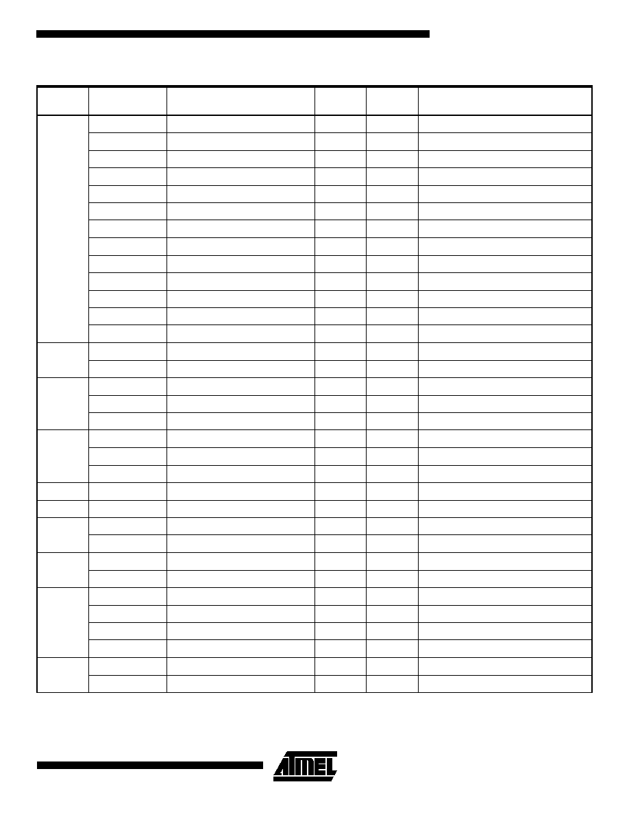
Table 1. AT91M40400 Pin Description
Module
Name
Function
Type
Active
Level
Comments
EBI
A0-A23
Address Bus
Output
--
All valid after reset
D0-D15
Data Bus
I/O
--
NCS0-NCS3
Chip Select
Output
low
CS4-CS7
Chip Select
Output
high
A23-A20 after reset
NWR0
Lower Byte 0 Write Signal
Output
low
Used in Byte Write Option
NWR1
Upper Byte 1 Write Signal
Output
low
Used in Byte Write Option
NRD
Read Signal
Output
low
Used in Byte Write Option
NWE
Write Enable
Output
low
Used in Byte Select Option
NOE
Output Enable
Output
low
Used in Byte Select Option
NUB
Upper Byte Select
Output
low
Used in Byte Select Option
NLB
Lower Byte Select
Output
low
Used in Byte Select Option
NWAIT
Wait Input
Input
low
BMS
Boot Mode Select
Input
--
Sampled during reset
AIC
FIQ
Fast Interrupt Request
Input
--
PIO controlled after reset
IRQ0-IRQ2
External Interrupt Request
Input
--
PIO controlled after reset
Timer
TCLK0-TCLK2
Timer External Clock
Input
--
PIO controlled after reset
TIOA0-TIOA2
Multipurpose Timer I/O pin A
I/O
--
PIO controlled after reset
TIOB0-TIOB2
Multipurpose Timer I/O pin B
I/O
--
PIO controlled after reset
USART
SCK0-SCK1
External Serial Clock
I/O
--
PIO controlled after reset
TXD0-TXD1
Transmit Data Output
Output
--
PIO controlled after reset
RXD0-RXD1
Receive Data Input
Input
--
PIO controlled after reset
PIO
P0-P31
Parallel IO line
I/O
--
WD
NWDOVF
Watchdog overflow
Output
low
Open drain
Clock
MCKI
Master Clock Input
Input
--
Schmidt trigger
MCKO
Master Clock Output
Output
--
Reset
NRST
Hardware Reset Input
Input
low
Schmidt trigger, internal pull-up
NTRI
Tristate Mode Select
Input
low
Sampled during reset
ICE
TMS
Test Mode Select
Input
--
Schmidt trigger, internal pull-up
TDI
Test Data Input
Input
--
Schmidt trigger, internal pull-up
TDO
Test Data Output
Output
--
TCK
Test Clock
Input
--
Schmidt trigger, internal pull-up
Power
VDD
Power
GND
Ground

AT91M40400
4
Block Diagram
Figure 2. AT91M40400 Block Diagram
ARM7TDMI Core
Embedded
ICE
Reset
EBI: External Bus Interface
RAM
4K bytes
ASB
Controller
Clock
AIC: Advanced
Interrupt Controller
AMBA Bridge
EBI User
Interface
TC: Timer
Counter
TC0
TC1
TC2
USART0
USART1
2 PDC
Channels
2 PDC
Channels
PIO: Parallel I/O Controller
PS: Power Saving
Chip ID
WD: Watchdog
Timer
APB
ASB
P
I
O
P
I
O
NRST
D0-D15
A1-A19
A0/NLB
NRD/NOE
NWR0/NWE
NWR1/NUB
NWAIT
NCS0
NCS1
P26/NCS2
P27/NCS3
P28/A20/CS7
P29/A21/CS6
P30/A22/CS5
P31/A23/CS4
P0/TCLK0
P3/TCLK1
P6/TCLK2
P1/TIOA0
P2/TIOB0
P4/TIOA1
P5/TIOB1
P7/TIOA2
P8/TIOB2
NWDOVF
TMS
TDO
TDI
TCK
MCKI
P25/MCKO
P12/FIQ
P9/IRQ0
P10/IRQ1
P11/IRQ2
P13/SCK0
P14/TXD0
P15/RXD0
P20/SCK1
P21/TXD1/NTRI
P22/RXD1
P16
P17
P18
P19
P23
P24/BMS

AT91M40400
5
Architectural Overview
The AT91M40400 architecture consists of two main buses,
the Advanced System Bus (ASB) and the Advanced
Peripheral Bus (APB). The ASB is designed for maximum
performance. It interfaces the processor with the on-chip
32-bit memories and the external memories and devices by
means of the External Bus Interface (EBI). The APB is
designed for accesses to on-chip peripherals and is opti-
mized for low power consumption. The AMBA Bridge pro-
vides an interface between the ASB and the APB.
An on-chip Peripheral Data Controller (PDC) transfers data
between the on-chip USARTs and the on and off-chip
memories without processor intervention. Most importantly,
the PDC removes the processor interrupt handling over-
head and significantly reduces the number of clock cycles
required for a data transfer. It can transfer up to 64k contig-
uous bytes without reprogramming the starting address. As
a re sult, the perfo rm ance of t he microcontrolle r is
increased and the power consumption reduced.
The AT91M40400 peripherals are designed to be pro-
grammed with a minimum number of instructions. Each
peripheral has a 16K byte address space allocated in the
upper 3M bytes of the 4G byte address space. Except for
the interrupt controller, the peripheral base address is the
lowest address of its memory space. The peripheral regis-
ter set is composed of control, mode, data, status and inter-
rupt registers.
To maximize the efficiency of bit manipulation, frequently
written registers are mapped into three memory locations.
The first address is used to set the individual register bits,
the second resets the bits and the third address reads the
value stored in the register. A bit can be set or reset by writ-
ing a one to the corresponding position at the appropriate
address. Writing a zero has no effect. Individual bits can
thus be modified without having to use costly read-modify-
write and complex bit manipulation instructions.
All of the external signals of the on-chip peripherals are
under the control of the Parallel I/O controller. The PIO
controller can be programmed to insert an input filter on
each pin or generate an interrupt on a signal change. After
reset, the user must carefully program the PIO Controller in
order to define which peripheral signals are connected with
off-chip logic.
The ARM7TDMI processor operates in little-endian mode
in the AT91M40400 microcontroller. The processor's inter-
nal architecture and the ARM and Thumb instruction sets
are described in the ARM7TDMI Datasheet. The on-chip
peripherals are described in the subsequent sections of
this datasheet. Electrical characteristics are documented in
a separate datasheet entitled "AT91M40400 Electrical and
Mechanical Characteristics".
The ARM Standard In-Circuit-Emulation debug interface is
supported via the ICE port of the AT91M40400 microcon-
troller. (This is not a standard IEEE 1149.1 JTAG Boundary
Scan interface)
PDC: Peripheral Data Controller
The AT91M40400 has a 4-channel PDC dedicated to the
two on-chip USARTs. One PDC channel is connected to
the receiving channel and one to the transmitting channel
of each USART.
The user interface of a PDC channel is integrated in the
memory space of each USART channel. It contains a 32-bit
address pointer register (US_RPR or US_TPR) and a 16-
bit byte count register (US_RCR or US_TCR). When the
programmed number of bytes are transferred, an end of
transfer interrupt is generated by the corresponding
USART.