1
Features
�
Incorporates the ARM7TDMI
TM
ARM
�
Thumb
�
Processor Core
� High-performance 32-bit RISC Architecture
� High-density 16-bit Instruction Set
� Leader in MIPS/Watt
� Embedded ICE (In-Circuit Emulation)
�
On-chip SRAM and/or ROM
� 32-bit Data Bus
� Single-clock Cycle Access
�
Fully Programmable External Bus Interface (EBI)
� Maximum External Address Space of 64M Bytes
� Up to 8 Chip Selects
� Software Programmable 8/16-bit External Databus
�
8-level Priority, Individually Maskable, Vectored Interrupt Controller
� 4 External Interrupts, Including a High-priority Low-latency Interrupt Request
�
32 Programmable I/O Lines
�
3-channel 16-bit Timer/Counter
� 3 External Clock Inputs
� 2 Multi-purpose I/O Pins per Channel
�
2 USARTs
� 2 Dedicated Peripheral Data Controller (PDC) Channels per USART
�
Programmable Watchdog Timer
�
Advanced Power-saving Features
� CPU and Peripheral Can be Deactivated Individually
�
Available in a 100-lead TQFP Package
Description
The AT91X40 Series is a subset of the Atmel AT91 16/32-bit microcontroller family,
which is based on the ARM7TDMI processor core. This processor has a high-perfor-
mance 32-bit RISC architecture with a high-density 16-bit instruction set and very low
power consumption. In addition, a large number of internally banked registers result in
very fast exception handling, making the device ideal for real-time control applications.
The AT91X40 Series features a direct connection to off-chip memory, including Flash,
through the fully programmable External Bus Interface (EBI). An eight-level priority
vectored interrupt controller, in conjunction with the Peripheral Data Controller signifi-
cantly improve the real-time performance of the device.
The devices are manufactured using Atmel's high-density CMOS technology. By com-
bining the ARM7TDMI processor core with on-chip high-speed memory and a wide
range of peripheral functions on a monolithic chip, the Atmel AT91X40 Series is a fam-
ily of powerful microcontrollers that offer a flexible, cost-effective solution to many
compute-intensive embedded control applications.
Microcontroller
Primary SRAM Bank
Secondary SRAM Bank
ROM
AT91M40800
8K Bytes
�
�
AT91R40807
8K Bytes
128K Bytes
�
AT91M40807
8K Bytes
�
128K Bytes
AT91R40008
256K Bytes
�
�
AT91
ARM
�
Thumb
�
Microcontrollers
AT91M40800
AT91R40807
AT91M40807
AT91R40008
Rev. 1354D�ATARM�05/02

3
AT91X40 Series
1354D�ATARM�05/02
Table 1. AT91X40 Series Pin Description
Module
Name
Function
Type
Active
Level
Comments
EBI
A0 - A23
Address Bus
Output
�
All valid after reset
D0 - D15
Data Bus
I/O
�
NCS0 - NCS3
Chip Select
Output
Low
CS4 - CS7
Chip Select
Output
High
A23 - A20 after reset
NWR0
Lower Byte 0 Write Signal
Output
Low
Used in Byte Write option
NWR1
Upper Byte 1 Write Signal
Output
Low
Used in Byte Write option
NRD
Read Signal
Output
Low
Used in Byte Write option
NWE
Write Enable
Output
Low
Used in Byte Select option
NOE
Output Enable
Output
Low
Used in Byte Select option
NUB
Upper Byte Select
Output
Low
Used in Byte Select option
NLB
Lower Byte Select
Output
Low
Used in Byte Select option
NWAIT
Wait Input
Input
Low
BMS
Boot Mode Select
Input
�
Sampled during reset
AIC
FIQ
Fast Interrupt Request
Input
�
PIO-controlled after reset
IRQ0 - IRQ2
External Interrupt Request
Input
�
PIO-controlled after reset
TC
TCLK0 - TCLK2
Timer External Clock
Input
�
PIO-controlled after reset
TIOA0 - TIOA2
Multipurpose Timer I/O Pin A
I/O
�
PIO-controlled after reset
TIOB0 - TIOB2
Multipurpose Timer I/O Pin B
I/O
�
PIO-controlled after reset
USART
SCK0 - SCK1
External Serial Clock
I/O
�
PIO-controlled after reset
TXD0 - TXD1
Transmit Data Output
Output
�
PIO-controlled after reset
RXD0 - RXD1
Receive Data Input
Input
�
PIO-controlled after reset
PIO
P0 - P31
Parallel IO Line
I/O
�
WD
NWDOVF
Watchdog Overflow
Output
Low
Open-drain
Clock
MCKI
Master Clock Input
Input
�
Schmidt trigger
MCKO
Master Clock Output
Output
�
Reset
NRST
Hardware Reset Input
Input
Low
Schmidt trigger
NTRI
Tri-state Mode Select
Input
Low
Sampled during reset
ICE
TMS
Test Mode Select
Input
�
Schmidt trigger, internal pull-up
TDI
Test Data Input
Input
�
Schmidt trigger, internal pull-up
TDO
Test Data Output
Output
�
TCK
Test Clock
Input
�
Schmidt trigger, internal pull-up
Power
VDDIO
I/O Power
Power
�
VDDCORE
Core Power
Power
�
GND
Ground
Ground
�

5
AT91X40 Series
1354D�ATARM�05/02
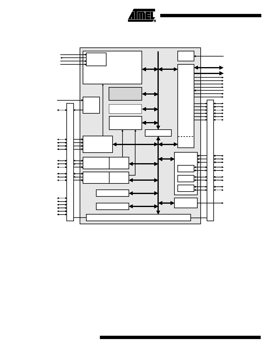
Architectural
Overview
The AT91X40 Series Microcontrollers integrate an ARM7TDMI with its embedded ICE
interface, memories and peripherals. The series' architecture consists of two main
buses, the Advanced System Bus (ASB) and the Advanced Peripheral Bus (APB).
Designed for maximum performance and controlled by the memory controller, the ASB
interfaces the ARM7TDMI processor with the on-chip 32-bit memories, the External Bus
Interface (EBI) and the AMBA
TM
Bridge. The AMBA Bridge drives the APB, which is
designed for accesses to on-chip peripherals and optimized for low-power consumption.
The AT91X40 Series Microcontrollers implement the ICE port of the ARM7TDMI proces-
sor on dedicated pins, offering a complete, low-cost and easy-to-use debug solution for
target debugging.
Memories
The AT91X40 Series Microcontrollers embed up to 256K bytes of internal SRAM, and
up to 128K bytes of ROM. The internal memories are directly connected to the 32-bit
data bus and are single-cycle accessible. This provides maximum performance of 0.9
MIPS/MHz by using the ARM instruction set of the processor, minimizing system power
consumption and improving the performance of separate memory solutions.
The AT91X40 Series Microcontrollers feature an External Bus Interface (EBI), which
enables connection of external memories and application-specific peripherals. The EBI
supports 8- or 16-bit devices and can use two 8-bit devices to emulate a single 16-bit
device. The EBI implements the early read protocol, enabling faster memory accesses
than standard memory interfaces.
Peripherals
The AT91X40 Series Microcontrollers integrate several peripherals, which are classified
as system or user peripherals. All on-chip peripherals are 32-bit accessible by the
AMBA Bridge, and can be programmed with a minimum number of instructions. The
peripheral register set is composed of control, mode, data, status and enable/dis-
able/status registers.
An on-chip Peripheral Data Controller (PDC) transfers data between the on-chip
USARTs and on- and off-chip memories address space without processor intervention.
Most importantly, the PDC removes the processor interrupt handling overhead, making
it possible to transfer up to 64K continuous bytes without reprogramming the start
address, thus increasing the performance of the microcontroller, and reducing the power
consumption.
System Peripherals
The External Bus Interface (EBI) controls the external memory or devices via an 8-bit or
16-bit data bus, and is programmed through the Advanced Peripheral Bus (APB). Each
chip select line has its own programming register.
The Power Saving (PS) module implements the Idle Mode (ARM7TDMI core clock
stopped until the next interrupt) and enables the user to adapt the power consumption of
the microcontroller to application requirements (independent peripheral clock control).
The Advanced Interrupt Controller (AIC) controls the internal sources from the internal
peripherals and the four external interrupt lines (including the FIQ) to provide an inter-
rupt and/or fast interrupt request to the ARM7TDMI. It integrates an 8-level priority
controller, and, using the Auto-vectoring feature, reduces the interrupt latency time.
The Parallel Input/Output Controller (PIO) controls up to 32 I/O lines. It enables the user
to select specific pins for on-chip peripheral input/output functions, and general-purpose
input/output signal pins. The PIO controller can be programmed to detect an interrupt on
a signal change from each line.