 | –≠–ª–µ–∫—Ç—Ä–æ–Ω–Ω—ã–π –∫–æ–º–ø–æ–Ω–µ–Ω—Ç: ATV750-25 | –°–∫–∞—á–∞—Ç—å:  PDF PDF  ZIP ZIP |
1
Features
∑
Advanced, High-speed Programmable Logic Device ≠ Superset of 22V10
≠ Improved Performance - 7.5 ns t
PD
, 95 MHz External Operation
≠ Enhanced Logic Flexibility
≠ Backward Compatible with ATV750(L) Software and Hardware
∑
New Flip-flop Features
≠ D- or T-type
≠ Product Term or Direct Input Pin Clocking
∑
High-speed Erasable Programmable Logic Devices
≠ 7.5 ns Maximum Pin-to-pin Delay
∑
Highest Density Programmable Logic Available in a 24-pin Package
∑
Increased Logic Flexibility
≠ 42 Array Inputs, 20 Sum Terms and 20 Flip-flops
∑
Enhanced Output Logic Flexibility
≠ All 20 Flip-flops Feed Back Internally
≠ 10 Flip-flops are Also Available as Outputs
∑
Full Military, Commercial and Industrial Temperature Ranges
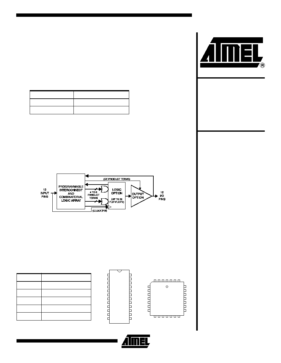
Logic Diagram
Description
The ATV750B(L) is twice as powerful as most other 24-pin programmable logic
devices. Increased product terms, sum terms, flip-flops and output logic configurations
translate into more usable gates. High-speed logic and uniform, predictable delays
guarantee fast in-system performance.
Device
I
CC
, Standby
ATV750B
125 mA
ATV750BL
15 mA
High-speed UV
Erasable
Programmable
Logic Device
ATV750B
ATV750BL
Commercial and
industrial versions
are obsolete. Please
use ATF750C.
Military versions
continue to be available,
but please do not
use for new designs.
For new military
applications, recommend
multiple ATF22V10s.
Rev. 0301I≠08/01
Pin Configurations
Pin Name
Function
CLK
Clock
IN
Logic Inputs
I/O
Bi-directional Buffers
*
No Internal Connection
V
CC
+5V Supply
DIP/SOIC
1
2
3
4
5
6
7
8
9
10
11
12
24
23
22
21
20
19
18
17
16
15
14
13
CLK/IN
IN
IN
IN
IN
IN
IN
IN
IN
IN
IN
GND
VCC
I/O
I/O
I/O
I/O
I/O
I/O
I/O
I/O
I/O
I/O
IN
PLCC/LCC
5
6
7
8
9
10
11
25
24
23
22
21
20
19
IN
IN
IN
*
IN
IN
IN
I/O
I/O
I/O
*
I/O
I/O
I/O
4
3
2
1
28
27
26
12
13
14
15
16
17
18
IN
IN
GND
*
IN
I/O
I/O
IN
IN
CLK/IN
*
VCC
I/O
I/O
2
ATV750B(L)
0301I≠08/01
Each of the ATV750B(L) 22 logic pins can be used as an input. Ten of these can be used as
inputs, outputs or bi-directional I/O pins. Each flip-flop is individually configurable as either D-
or T-type. Each flip-flop output is fed back into the array independently. This allows burying of
all the sum terms and flip-flops.
There are 171 total product terms available. A variable format is used to assign between four
to eight product terms per sum term. There are two sum terms per output, providing added
flexibility. Much more logic can be replaced by this device than by any other 24-pin PLD. With
20 sum terms and flip-flops, complex state machines are easily implemented with logic to
spare.
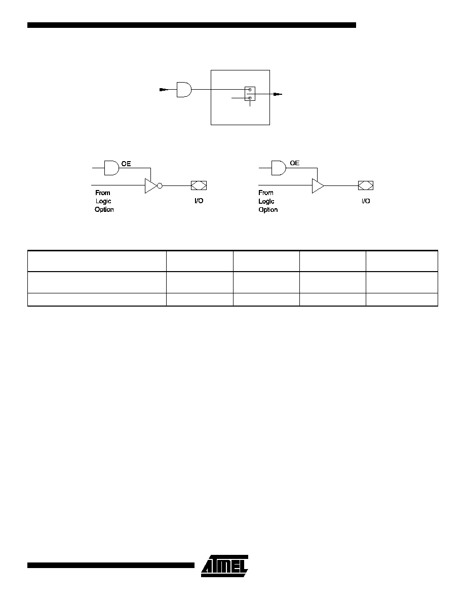
Product terms provide individual clocks and asynchronous resets for each flip-flop. Each flip-
flop may also be individually configured to have direct input pin controlled clocking. Each out-
put has its own enable product term. One product term provides a common synchronous
preset for all flip-flops. Register preload functions are provided to simplify testing. All registers
automatically reset upon power-up.
The ATV750BL is a low-power device with speeds as fast as 15 ns. The ATV750BL provides
the optim um low-power PLD solution, with full CMOS output levels. This device
significantly reduces total system power, thereby allowing battery-powered operation.
Logic Options
Absolute Maximum Ratings*
Temperature Under Bias................................ -55∞C to +125∞C
*NOTICE:
Stresses beyond those listed under "Absolute
Maximum Ratings" may cause permanent dam-
age to the device. This is a stress rating only and
functional operation of the device at these or any
other conditions beyond those indicated in the
operational sections of this specification is not
implied. Exposure to absolute maximum rating
conditions for extended periods may affect
device reliability.
Note:
1. Minimum voltage is -0.6V DC which may under-
shoot to -2.0V for pulses of less than
20 ns.Maximum output pin voltage is V
CC
+ 0.75V
DC which may overshoot to +7.0V for pulses of
less than 20 ns.
Storage Temperature ..................................... -65∞C to +150∞C
Voltage on Any Pin with
Respect to Ground .........................................-2.0V to +7.0V
(1)
Voltage on Input Pins
with Respect to Ground
During Programming.....................................-2.0V to +14.0V
(1)
Programming Voltage with
Respect to Ground .......................................-2.0V to +14.0V
(1)
Integrated UV Erase Dose..............................7258 W
∑
sec/cm
2
Combinatorial Output
Combined Terms
Separate Terms
Registered Output
Combined Terms
Separate Terms
3
ATV750B(L)
0301I≠08/01
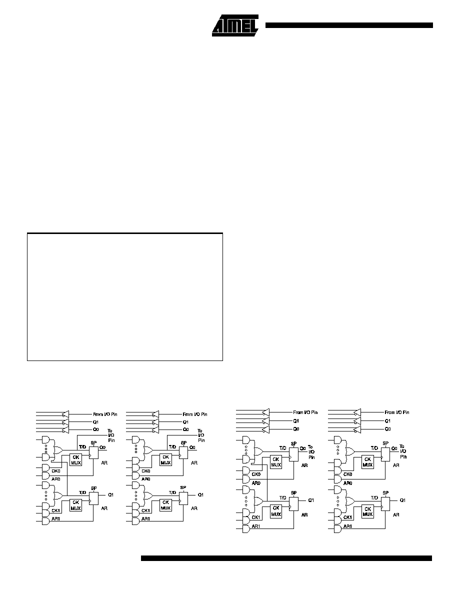
Clock Mux
Output Options
Note:
1. See ordering information for valid speed and temperature combination.
SELECT
LOGIC
TO
CELL
CLOCK
PRODUCT
TERM
CLK
CKi
CK MUX
PIN
DC and AC Operating Conditions
(1)
Commercial
-7, -10, -15
Commercial
-25
Industrial
Military
Operating Temperature
0∞C - 70∞C
(Ambient)
0∞C - 70∞C
(Ambient)
-40∞C - 85∞C
(Ambient)
-55∞C - 125∞C
(Case)
V
CC
Power Supply
5V
± 5%
5V
± 10%
5V
± 10%
5V
± 10%
4
ATV750B(L)
0301I≠08/01
Note:
1. Not more than one output at a time should be shorted. Duration of short circuit test should not exceed 30 sec.
DC Characteristics
Symbol
Parameter
Condition
Min
Typ
Max
Units
I
LI
Input Load Current
V
IN
= -0.1V to V
CC
+ 1V
10
µA
I
LO
Output Leakage
Current
V
OUT
= -0.1V to V
CC
+ 0.1V
10
µA
I
CC
Power Supply
Current, Standby
V
CC
= MAX,
V
IN
= MAX,
Outputs Open
B-7, -10
Com.
125
180
mA
Ind., Mil.
125
190
mA
B-15, -25
Com.
125
180
mA
Ind., Mil.
125
190
mA
BL-15
Com.
15
30
mA
Ind., Mil.
15
30
mA
I
OS
(1)
Output Short
Circuit Current
V
OUT
= 0.5V
-120
mA
V
IL
Input Low Voltage
4.5
V
CC
5.5V
-0.6
0.8
V
V
IH
Input High Voltage
2.0
V
CC
+ 0.75
V
V
OL
Output Low
Voltage
V
IN
= V
IH
or V
IL
,
V
CC
= MIN
I
OL
= 16 mA
Com., Ind.
0.5
V
I
OL
= 12 mA
Mil.
0.5
V
I
OL
= 24 mA
Com.
0.8
V
V
OH
Output High
Voltage
V
IN
= V
IH
or V
IL
,
V
CC
= MIN
I
OH
= -100
µA
V
CC
- 0.3
V
I
OH
= -4.0 mA
2.4
V
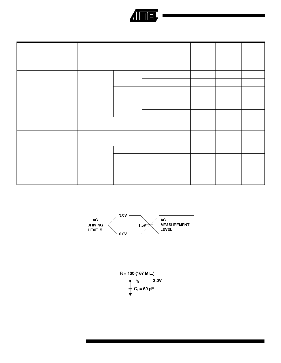
Input Test Waveforms and Measurement Levels
t
R
, t
F
< 3 ns (10% to 90%)
Output Test Load
5
ATV750B(L)
0301I≠08/01
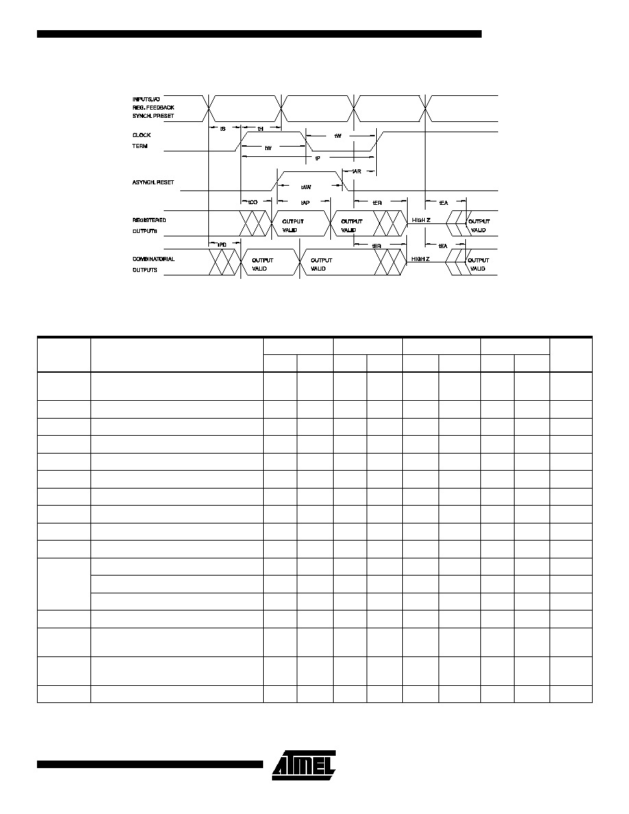
AC Waveforms, Product Term Clock
(1)
Note:
1. Timing measurement reference is 1.5V. Input AC driving levels are 0.0V and 3.0V, unless otherwise specified.
Note:
1. See ordering information for valid part numbers.
AC Characteristics, Product Term Clock
(1)
Symbol
Parameter
-7
-10
B/BL-15
B/BL-25
Units
Min
Max
Min
Max
Min
Max
Min
Max
t
PD
Input or Feedback to
Non-Registered Output
7.5
10
15
25
ns
t
EA
Input to Output Enable
7.5
10
15
25
ns
t
ER
Input to Output Disable
7.5
10
15
25
ns
t
CO
Clock to Output
3
7.5
4
10
5
12
6
20
ns
t
CF
Clock to Feedback
1
5
4
7.5
5
9
5
10
ns
t
S
Input Setup Time
3
4
8/12
14
ns
t
SF
Feedback Setup Time
3
4
7
7
ns
t
H
Hold Time
1
2
5/7
5/7
ns
t
P
Clock Period
7
11
14
17
ns
t
W
Clock Width
3.5
5.5
7
8.5
ns
f
MAX
External Feedback 1/(t
S
+t
CO
)
95
71
50/41
29
MHz
Internal Feedback 1/(t
SF
+t
CF
)
125
86
62
58
MHz
No Feedback 1/(t
P
)
142
90
71
58
MHz
t
AW
Asynchronous Reset Width
5
10
15
20
ns
t
AR
Asynchronous Reset
Recovery Time
3
10
15
20
ns
t
AP
Asynchronous Reset to
Registered Output Reset
8
12
15
25
ns
t
SP
Setup Time, Synchronous Preset
4
7
8
15
ns