1
Features
∑
Third Generation Programmable Logic Structure
≠ High-Density Replacement for Discrete Logic
∑
High-Speed -- Plus a New, Low-Power Version
∑
Increased Logic Flexibility
≠ 42 Inputs and 20 Sum Terms
∑
Flexible Output Logic
≠ 20 Flip-Flops - 10 Extra
≠ All Can Be Individually Buried or 10 Output Directly
≠ Each has Individual Asynchronous Reset and Clock Terms
∑
Multiple Feedback Paths Provide for Buried State Machines
and I/O Bus Compatibility
∑
Proven and Reliable High-Speed CMOS EPROM Process
≠ 2000V ESD Protection
≠ 200 mA Latchup Immunity
∑
Reprogrammable
≠ Tested 100% for Programmability
∑
24-pin, 300-mil Dual-In-line and 28-Lead Surface Mount Packages
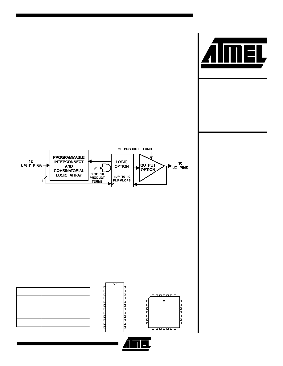
Logic Diagram
Description
The ATV750(L) is 100% more powerful than most other programmable logic devices
in 24-pin packages. Increased product terms, sum terms, and flip-flops translate into
more usable gates.
Each of the ATV750(L)'s twenty-two logic pins can be used as an input. Ten of these
can be used as input, output, or bi-directional I/O pins. All twenty flip-flops can be fed
back into the array independently. This flexibility allows burying all of the sum terms
and flip-flops.
There are 171 product terms available. A variable format is used to assign between
four and eight product terms per sum term. There are two sum terms per output, pro-
viding added flexibility.
Rev. 0024E≠05/98
Pin Configurations
Pin Name
Function
IN
Logic Inputs
I/O
Bidirectional Buffers
*
No Internal Connection
VCC
+5V Supply
(continued)
High Density UV
Erasable
Programmable
Logic Device
ATV750
ATV750L
DIP/SOIC
1
2
3
4
5
6
7
8
9
10
11
12
24
23
22
21
20
19
18
17
16
15
14
13
IN
IN
IN
IN
IN
IN
IN
IN
IN
IN
IN
GND
VCC
I/O
I/O
I/O
I/O
I/O
I/O
I/O
I/O
I/O
I/O
IN
PLCC/LCC
(Top View)
5
6
7
8
9
10
11
25
24
23
22
21
20
19
IN
IN
IN
*
IN
IN
IN
I/O
I/O
I/O
*
I/O
I/O
I/O
4
3
2
1
28
27
26
12
13
14
15
16
17
18
IN
IN
GND
*
IN
I/O
I/O
IN
IN
IN
*
VCC
I/O
I/O
ATV750/L
2
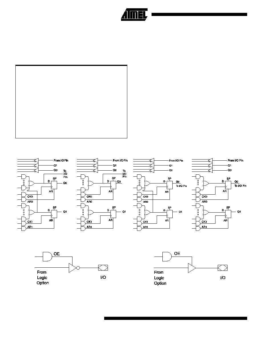
The ATV750(L) has more flip-flops available than other
PLDs in this density range. Complex state machines are
easily implemented.
Product terms are available providing asynchronous
resets, flip-flop clocks, and output enables. One reset and
one clock term are provided per flip-flop, with one enable
term per output. One product term provides a global syn-
chronous preset. Register preload simplifies testing. The
device has an internal power up clear function.
Logic Options
Output Options
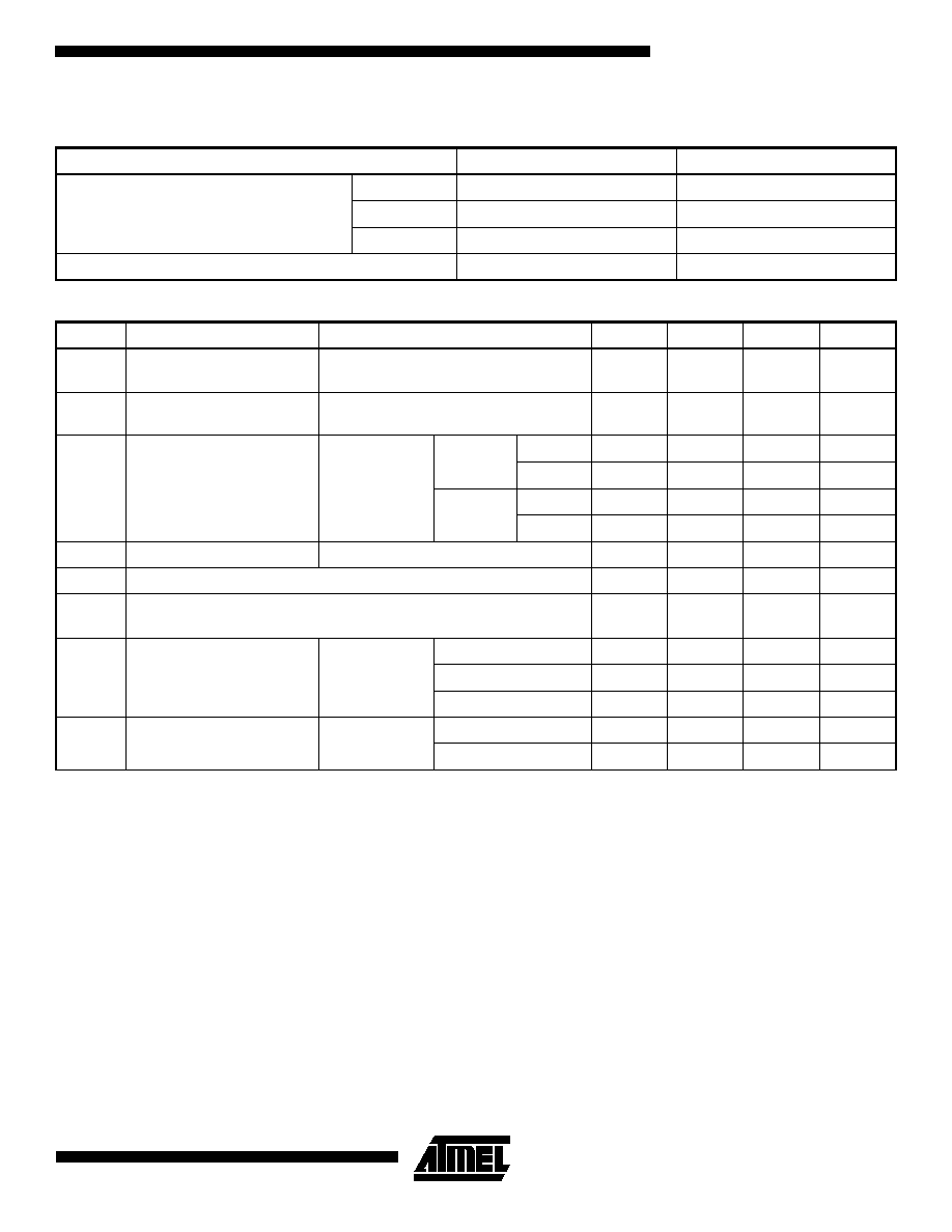
Absolute Maximum Ratings
Temperature Under Bias ............................... -55∞C to + 125∞C
*NOTICE:
Stresses beyond those listed under "Absolute
Maximum Ratings" may cause permanent dam-
age to the device. This is a stress rating only and
functional operation of the device at these or any
other conditions beyond those indicated in the
operational sections of this specification is not
implied. Exposure to absolute maximum rating
conditions for extended periods may affect device
reliability.
Note:
1.
Minimum voltage is -0.6V DC, which may under-
shoot to -2.0V for pulses of less than 20 ns. Max-
imum output pin voltage is Vcc + 0.75V DC,
which may overshoot to 7.0V for pulses of less
than 20 ns.
Storage Temperature .................................... -65∞C to + 150∞C
Voltage on Any Pin with
Respect to Ground .........................................-2.0V to +7.0V
(1)
Voltage on Input Pins
with Respect to Ground
During Programming.....................................-2.0V to +14.0V
(1)
Programming Voltage with
Respect to Ground .......................................-2.0V to +14.0V
(1)
Integrated UV Erase Dose.............................. 7258 W.sec/cm
2
Combined Terms
Separate Terms
Combined Terms
Separate Terms
ATV750/L
3
Note:
1. Not more than one output at a time should be shorted. Duration of short circuit test should not exceed 30 sec.
DC and AC Operating Conditions
ATV750-20
ATV750/750L-25
Operating Temperature (Case)
Com.
0∞C - 70∞C
0∞C - 70∞C
Ind.
-40∞C - 85∞C
-40∞C - 85∞C
Mil.
-55∞C - 125∞C
-55∞C - 125∞C
V
CC
Power Supply
5V
±
10%
5V
±
10%
DC Characteristics
Symbol
Parameter
Condition
Min
Typ
Max
Units
I
LI
Input Load
Current
V
IN
= -0.1V to V
CC
+ 1V
10
µ
A
I
LO
Output Leakage
Current
V
OUT
= -0.1V to V
CC
+ 0.1V
10
µ
A
I
CC
Power Supply
Current
V
CC
= MAX,
V
IN
= GND,
Outputs Open
ATV750
Com.
120
mA
Ind.,Mil.
140
mA
ATV750L
Com.
1.0
12
mA
Ind.,Mil.
1.0
15
mA
I
OS
(1)
Output Short Circuit Current
V
OUT
= 0.5V
-120
mA
V
IL
Input Low Voltage
-0.6
0.8
V
V
IH
Input High Voltage
2.0
V
CC
+
0.75
V
V
OL
Output Low Voltage
V
IN
= V
IH
or V
IL
,
V
CC
= MIN
I
OL
= 12 mA Com.,Ind.
0.5
V
I
OL
= 8 mA Mil.
0.5
V
I
OL
= 24 mA, Com.
1.0
V
V
OH
Output High Voltage
V
IN
= V
IH
or V
IL
,
V
CC
= MIN
I
OH
= -100
µ
A
V
CC
- 0.3
V
I
OH
= -4.0 mA
2.4
V
ATV750/L
4
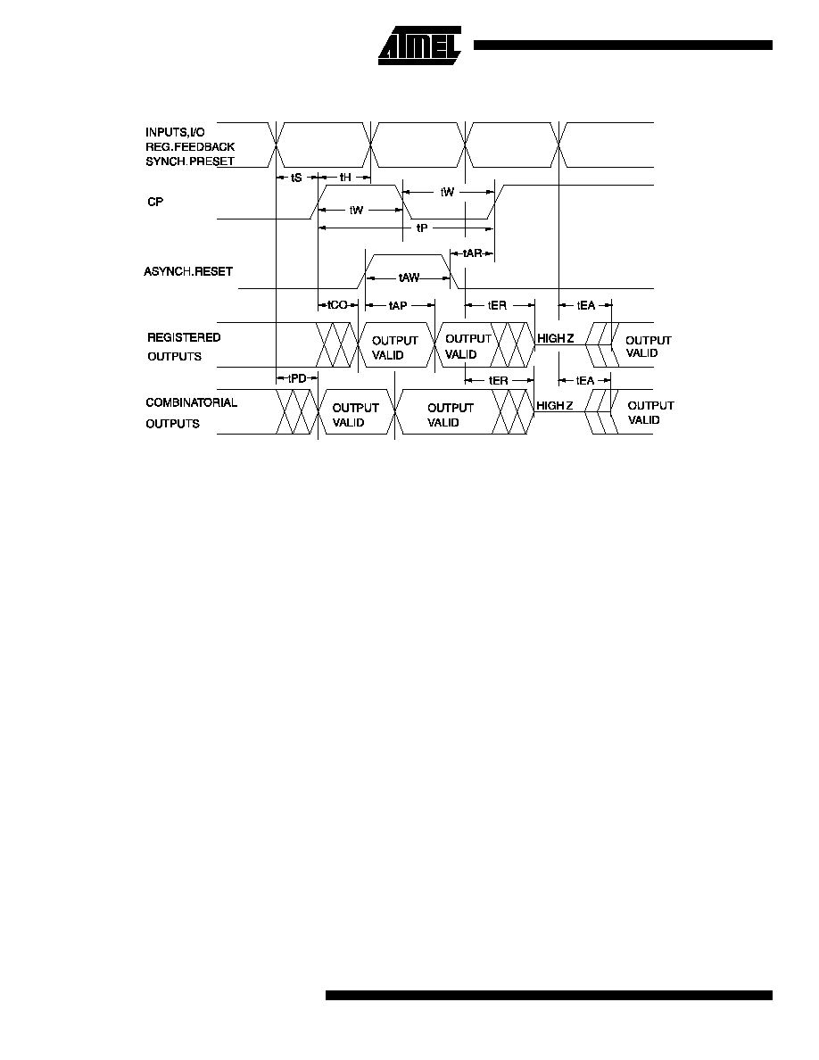
AC Waveforms
(1)
Note:
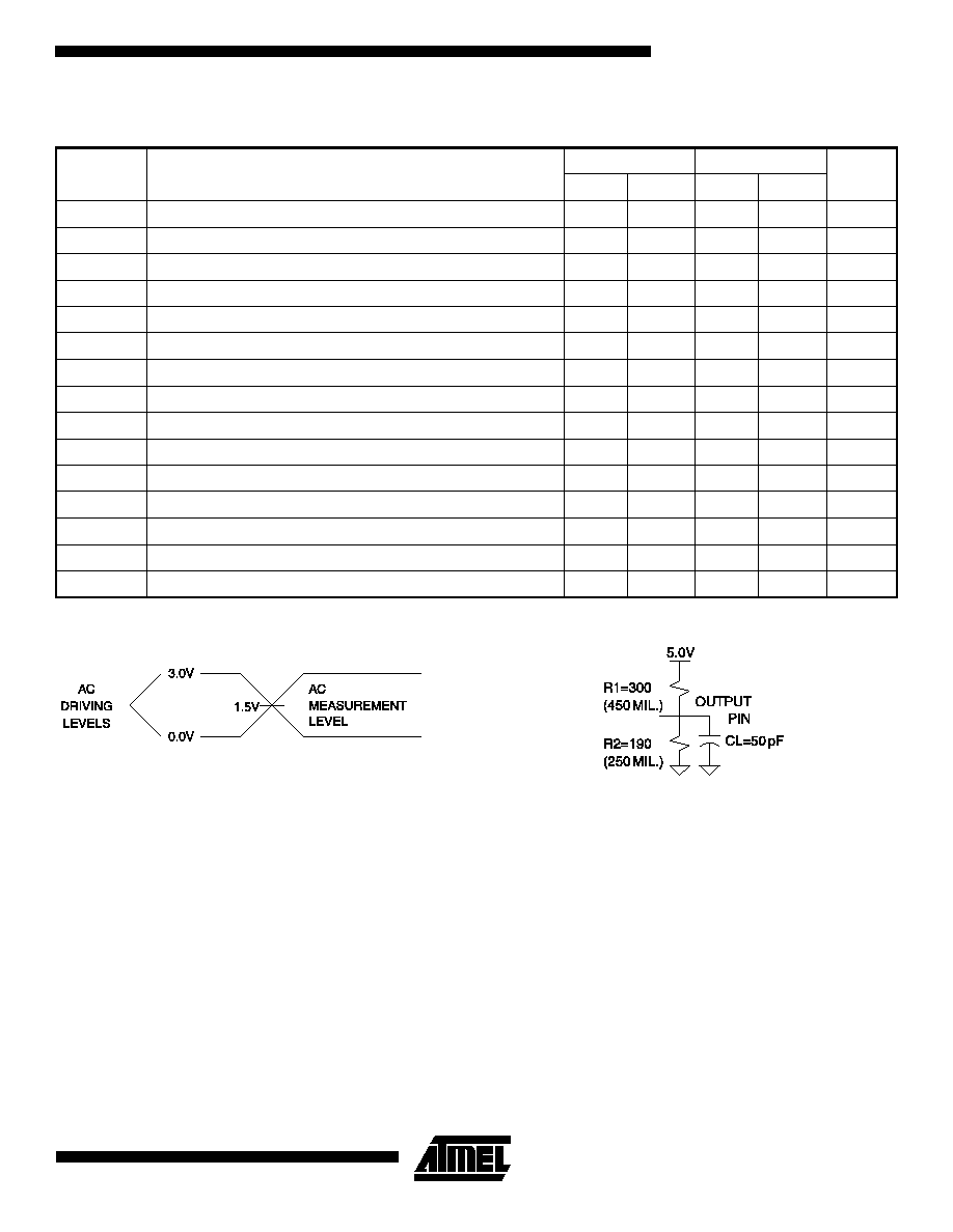
1.
Timing measurement reference is 1.5V. Input AC driving levels are 0.0V and 3.0V, unless otherwise specified.
ATV750/L
5
Input Test Waveforms and
Measurement Levels
t
R
, t
F
< 5 ns (10% to 90%)
Output Test Loads
AC Characteristics
Symbol
Parameter
ATV750-20
ATV750/750L-25
Units
Min
Max
Min
Max
t
PD
Input or Feedback to Non-Registered Output
20
25
ns
t
EA
Input to Output Enable
20
25
ns
t
ER
Input to Output Disable
20
25
ns
t
CO
Clock to Output
20
22
ns
t
CF
Clock to Feedback
5
10
5
10
ns
t
S
Input Setup Time
10
12
ns
t
SF
Feedback Setup Time
5
7
ns
t
H
Hold Time
5
5
ns
t
P
Clock Period
18
22
ns
t
W
Clock Width
8
10
ns
F
MAX
Maximum Frequency
55
45
MHz
t
AW
Asynchronous Reset Width
15
20
ns
t
AR
Asynchronous Reset Recovery Time
15
20
ns
t
AP
Asynchronous Reset to Registered Output Reset
20
25
ns
t
SP
Setup Time, Synchronous Preset
12
15
ns