Rev. 4142B≠AERO≠06/02
1
Features
∑
Comprehensive Library of Standard Logic Cells
∑
MH2RT I/O Cells Designed to Operate With VDD 2.5V + 0.2V as Main Target Operating
Conditions
∑
IO33 Pad Library Provides Interface to 3.3V Environment
∑
Memory Cells Compiled to Precise Design Requirements
∑
Processed on Radiation Hard 0.25 µm CMOS Process, 5 Metal Layers
∑
Cold Sparing Buffers
∑
Pre-defined Pads Frames
∑
SEU Free Cells
∑
Latch-up Immune
∑
200 Krads Total Dose
∑
LVDS, LVTTL, PCI, PECL Buffers
∑
75 µm Buffer Pitch Allowing up to 750 pads
∑
High Speed: <100 ps Typical Propagation Gate Delay (NAND2 with FO = 2)
∑
Integration Capability With up to 5 Mgates
∑
Up to 2.25-Mbit Memory Compiler
∑
MQFP Package With Pin Count up to 352
∑
CLGA Packages With 1.25 mm and 1 mm Column Pitches and Pin Count up to 613
Description
The Atmel MH2RT cell-based ASIC series are fabricated on a 0.25 micron CMOS pro-
cess, with up to five levels of metal. This family allows up to 5 million gates and 800
pads. The high density and high pin count capabilities of the MH2RT family, coupled
with the ability to embed processor cores or memories on the same silicon, make the
MH2RT series an ideal choice for System Level Integration.
The MH2RT series is supported by an advanced software environment based on
industry standards linking proprietary and commercial tools. Verilog
Æ
, DFT, Synopsys
Æ
and Vital are the reference front-end tools. The Cadence
TM
"Logic Design Planner"
floor planning associated with timing driven layout provides an efficient back-end
cycle.
The MH2RT series comes as a dual use of the MH2 series adding:
- through process changes, the 100 MeV latch up immunity and the 200 Krads+
total dose capability as required by most of the space programs,
- through cells layout, an SEU immunity allowing to SEU harden only where it is
actually necessary with respect to function requirements.
The MH2RT series comes as the Atmel 8th generation of ASIC series designed for
radiation hardened applications in 19 years.
It will be made available to any of the currently available quality grades, including
QML Q and V.
The Atmel MH2RT family is fabricated on a proprietary 0.25 micron five-layer-metal
CMOS process intended for use with a supply voltage of 2.5V ± 0.2V.
The MH2RT Series is offered with a mutli-project wafer service.
Rad. Hard
5M Gates
0.25 µm CMOS
Cell-based
MH2RT
Advance
Information
2
MH2RT
4142B≠AERO≠06/02
The following table shows the range for which Atmel library cells have been
characterized.
The Atmel cell libraries and megacell compilers have been designed to be compatible
with each other. Simulation representations exist for three types of operating conditions.
They correspond to three characterization conditions defined as follows:
∑
MIN conditions:
TJ = -55
∞
C
VDD (cell) = 2.7V
Process = fast (military best case)
∑
TYP conditions:
TJ = +25
∞
C
VDD (cell) = 2.5V
Process = typ (military typical case)
∑
MAX conditions:
TJ = +125
∞
C
VDD (cell) = 2.3V
Process = slow (military worst case)
Delays to tri-state are defined as delays to turn off (VGS < VT) the driving devices. Out-
put pad drain current corresponds to the output current of the pad when the output
voltage is VOL or VOH. The output resistor of the pad and the voltage drop due to
access resistors (in and out of the die) are taken into account. In order to have accurate
timing estimates, all characterization has been run on electrical netlists extracted from
the layout database.
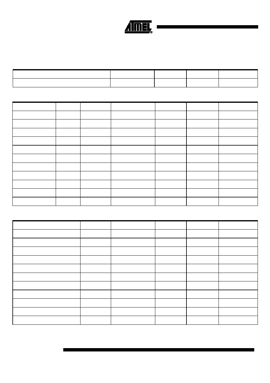
Table 1. Recommended Operating Conditions
Symbol
Parameter
Conditions
Min
Typ
Max
Unit
V
DD
DC Supply Voltage
Core and Standard I/Os
2.3
2.5
2.7
V
V
DD3
DC Supply Voltage
3V Interface I/Os
3
3.3
3.6
V
V
I
DC Input Voltage
0
V
DD
V
V
O
DC Output Voltage
0
V
DD
V
TEMP
Operating Free Air
Temperature Range
Military
-55
+125
∞
C
3
MH2RT
4142B≠AERO≠06/02
Standard Cell Library
The Atmel Standard Cell Library, contains a comprehensive set of combinational logic
and storage cells. The library includes cells which belong to the following categories:
∑
Buffers and Gates
∑
Multiplexers
∑
Flip-flops
∑
Scan Flip-flops
∑
Latches
∑
Adders and Subtractors
Decoding the Cell Name
The table below shows the naming conventions for the cells in the library. Each cell
name begins with either a two-, three-, or four-letter code that defines the type of cell.
This indicates the range of standard cells available.
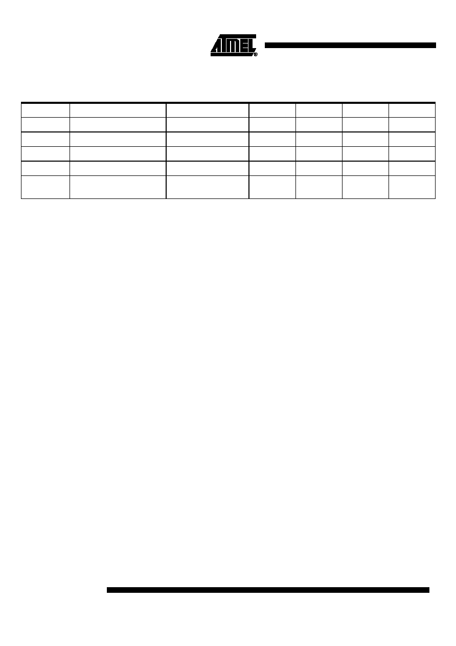
Table 2. Cell Codes
Code
Description
Code
Description
AD
Adder INVT
Inverting
3-State
Buffer
AH
Half Adder
JK
JK Flip-Flop
AS
Adder/Subtractor
LA
D Latch
AN
AND Gate
MI
Inverting Multiplexer
AOI
AND-OR-Invert Gate
MX
Multiplexer
AON
AND-OR-AND-Invert Gates
ND
NAND Gate
AOR
AND-OR Gate
NR
NOR Gate
BH
Bus Holder
OAI
OR-AND-Invert Gate
BUFB
Balanced Buffer
OAN
OR-AND-OR-Invert Gates
BUFF
Non-Inverting Buffer
OR
OR Gate
BUFT
Non-Inverting 3-State Buffer
ORA
OR-AND Gate
CG
Carry Generator
SD
Multiplexed Scan D Flip-Flop
CLK2
Clock Buffer
SE
Multiplexed Scan Enable D Flip-Flop
DE
D-Enabled Flip-Flop
SRLA
Set/Reset Latches with NAND input
DF
D Flip-Flop
SU
Subtractor
INV0
Inverter
XN
Exclusive NOR Gate
INVB
Balanced Inverter
XR
Exclusive OR Gate
5
MH2RT
4142B≠AERO≠06/02
Input/Output Pad Cell
Libraries IO25lib and
IO33lib
The Atmel Input/Output Cell Library, IO25lib, contains a comprehensive list of input, out-
put, bi-directional and tri-state cells. The MH2RT (2.5V) cell library includes a special set
of I/O cells, IO33lib, for interfacing with external 3.3V devices.
Voltage Levels
The IO25lib library is made up exclusively of low-voltage chip interface circuits powered
by a voltage in the range of 2.3V to 2.7V. The library is compatible with the 2.5V stan-
dard cells library.
Power and Ground Pads
Designers are strongly encouraged to provide three kinds of power pairs for the IO25lib
library. These are "AC", "DC" and core power pairs. AC power is used by the I/O to
switch its output from one state to the other. This switching generates noise in the AC
power buses on the chip. DC power is used by the I/O to maintain its output in a steady
state. The best noise performance is achieved when the DC power buses on the chip
are free of noise; designers are encouraged to use separate power pairs for AC and DC
power to prevent most of the noise in the AC power buses from reaching the DC power
buses. The same power pairs can be used to supply both DC power to the I/Os and
power to the core without affecting noise performance.
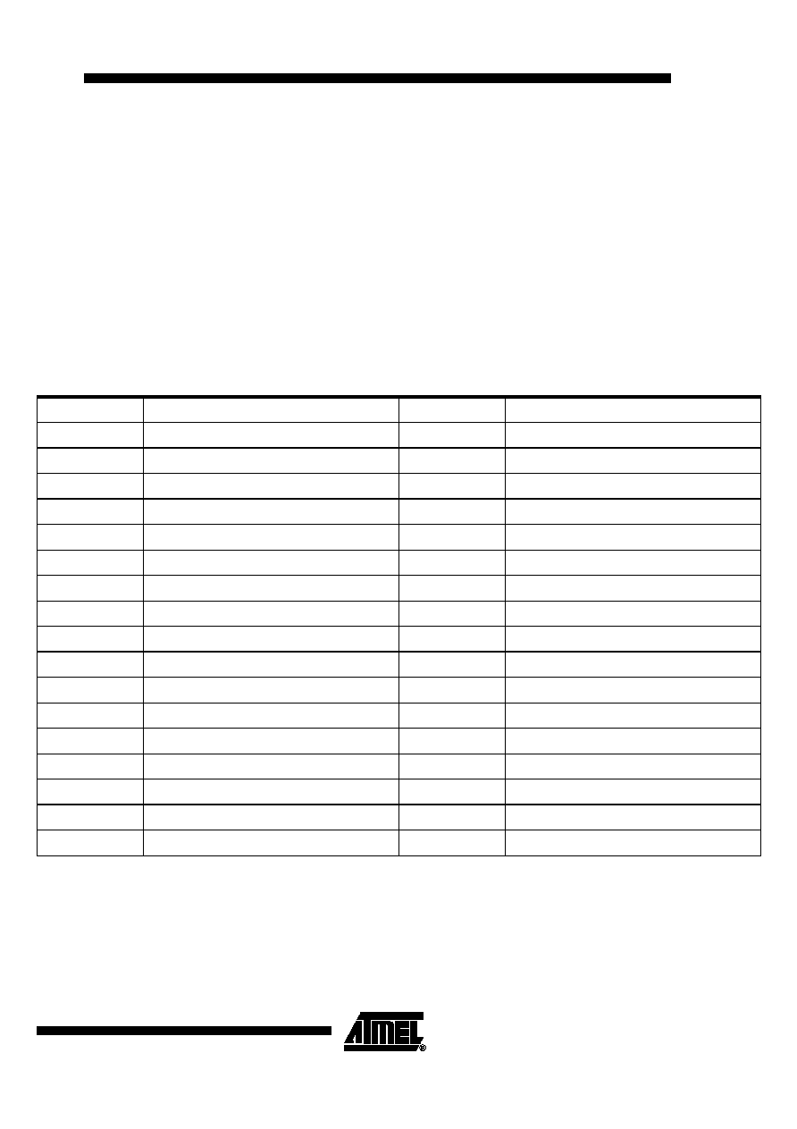
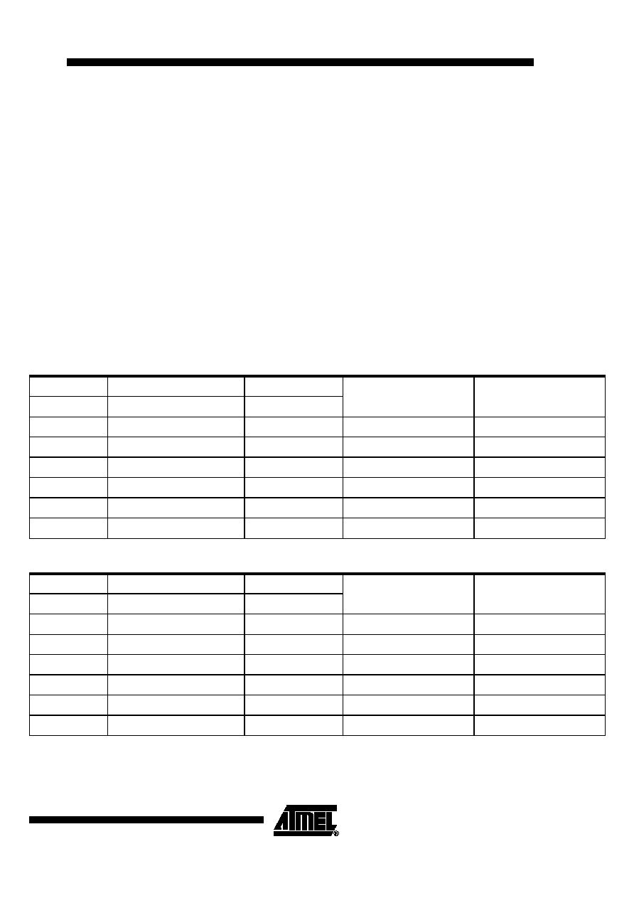
Table 6. VSS Power Pad Combinations
Core
Switching I/O
Quiet I/O
Library Cell Name
Signal Name
Vssi
VssAC
VssDC
∑
pv25i00
VSS
∑
pv25a00
VSS
∑
pv25d00
VSS
∑
∑
pv25e00
VSS
∑
∑
pv25b00
VSS
∑
∑
∑
pv25f00
VSS
Table 7. VDD Power Pad Combinations
Core
Switching I/O
Quiet I/O
Library Cell Name
Signal Name
Vddi
VddAC
VddDC
∑
pv25i25
VDD
∑
pv25a25
VDD
∑
pv25d25
VDD
∑
∑
pv25e25
VDD
∑
∑
pv25b25
VDD
∑
∑
∑
pv25f25
VDD