1
Features
∑
Carrier Frequency f
osc
100 kHz - 150 kHz
∑
Typical Data Rate up to 5 kbaud at 125 kHz
∑
Suitable for Manchester and Bi-phase Modulation
∑
Power Supply from the Car Battery or from 5-V Regulated Voltage
∑
Optimized for Car Immobilizer Applications
∑
Tuning Capability
∑
Microcontroller-compatible Interface
∑
Low Power Consumption in Standby Mode
∑
Power-supply Output for Microcontroller
Applications
∑
Car Immobilizers
∑
Animal Identification
∑
Access Control
∑
Process Control
Description
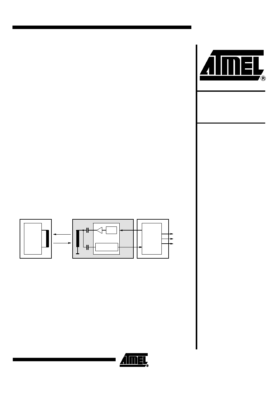
The U2270B is an IC for IDIC
“
read/write base stations in contactless identification
and immobilizer systems.
The IC incorporates the energy-transfer circuit to supply the transponder. It consists of
an on-chip power supply, an oscillator and a coil driver optimized for automotive-spe-
cific distances. It also includes all signal-processing circuits which are necessary to
transform the small input signal into a microcontroller-compatible signal.
System Block Diagram
enable
Read/write base station
MCU
Unlock
System
RF field
typ. 125 kHz
Transponder
IC
Transponder/TAG
Carrier
output
Data
NF read channel
Osc
U2270B
Read/Write
Base Station
U2270B
Rev. 4684A≠RFID≠02/03
4
U2270B
4684A≠RFID≠02/03
V
S
is the internal power supply voltage except for the driver circuit. Pin V
S
is used to con-
nect a block capacitor. V
S
can be switched off by Standby pin. In standby mode, the
chip's power consumption is very low. V
EXT
is the supply voltage of the antenna's pre-
driver. This voltage can also be used to operate external circuits, like a microcontroller.
In conjunction with an external NPN transistor it also establishes the supply voltage of
the antenna coil driver, DVS.
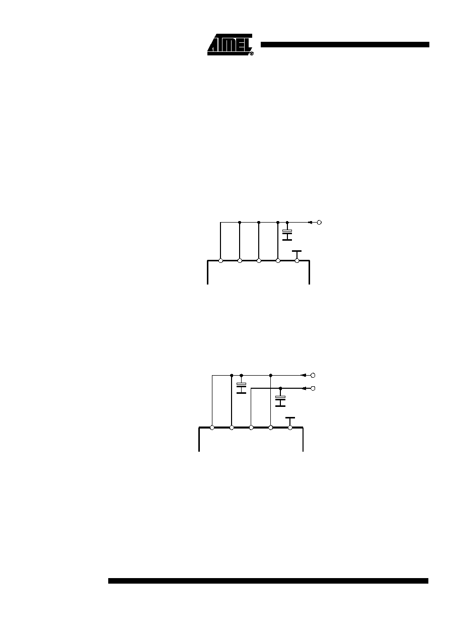
Operation Modes to
Power the U2270B
The following section explains the 3 different operation modes to power the U2270B.
One-rail Operation
All internal circuits are operated from one 5-V power rail (see Figure 3). In this case, V
S
,
V
EXT
and D
VS
serve as inputs. V
Batt
is not used but should also be connected to that sup-
ply rail.
Figure 3. One Rail Operation Supply
Two-rail Operation
In this application, the driver voltage, D
VS
, and the pre-driver supply, V
EXT
, are operated
at a higher voltage than the rest of the circuitry to obtain a higher driver-output swing
and thus a higher magnetic field (see Figure 4). V
S
is connected to a 5-V supply,
whereas the driver voltages can be as high as 8 V. This operation mode is intended to
be used in situations where an extended communication distance is required.
Figure 4. Two Rail Operation Supply
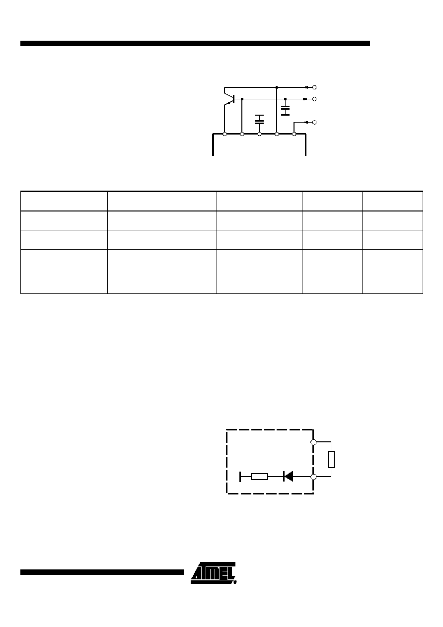
Battery-voltage Operation
Using this operation mode, V
S
and V
EXT
are generated by the internal power supply (see
Figure 5). For this mode, an external voltage regulator is not needed. The IC can be
switched off via the Standby pin. V
EXT
supplies the base of an external NPN transistor
and external circuits, like a microcontroller (even in Standby mode).
Pin V
EXT
and V
Batt
are overvoltage protected via internal Zener diodes (see Figure
2).The maximum current into the pins is determined by the maximum power dissipation
and the maximum junction temperature of the IC.
D
VS
V
EXT
V
S
V
Batt
Standby
+5 V (stabilized)
D
VS
V
EXT
V
S
V
Batt
Standby
5 V (stabilized)
7 to 8 V (stabilized)
5
U2270B
4684A≠RFID≠02/03
Figure 5. Battery Operation
Table 1. Characteristics of the Various Operation Modes
Oscillator (Osc)
The frequency of the on-chip oscillator is controlled by a current fed into the R
F
input. An
integrated compensation circuit ensures a wide temperature range and a supply-volt-
age-independent frequency which is selected by a fixed resistor between R
F
(pin 15)
and V
S
(pin 14). For 125 kHz, a resistor value of 110 k
W
is defined. For other frequen-
cies, use the following formula:
This input can be used to adjust the frequency close to the resonance of the antenna.
For more details refer to the section "Applicatons" and to the application note ANT019.
Figure 6. Equivalent Circuit of Pin R
F
D
VS
V
EXT
V
S
V
Batt
Standby
7 to 16 V
Operation Mode
External Components Required
Supply-voltage Range
Driver Output
Voltage Swing
Standby Mode
Available
One-rail operation
1 Voltage regulator
1 Capacitor
5 V
±
10%
ª
4 V
No
Two-rail operation
2 Voltage regulators
2 Capacitors
5 V
±
10%
7 V to 8 V
6 V to 7 V
No
Battery-voltage operation
1 Transistor
2 Capacitors Optional for load
dump protection:
1 Resistor
1 Capacitor
6 V to 16 V
ª
4 V
Yes
R
t
k
W
[
]
14375
f
0
kHz
[
]
---------------------
5
≠
=
V
S
R
F
2 k
W
R
f

