 | –≠–ª–µ–∫—Ç—Ä–æ–Ω–Ω—ã–π –∫–æ–º–ø–æ–Ω–µ–Ω—Ç: TISP820XM | –°–∫–∞—á–∞—Ç—å:  PDF PDF  ZIP ZIP |
MAY 1998 - REVISED FEBRUARY 2005
Specifications are subject to change without notice.
Customers should verify actual device performance in their specific applications.
TISP8200M & TISP8201M
TISP8200M, BUFFERED P-GATE SCR DUAL
TISP8201M, BUFFERED N-GATE SCR DUAL
COMPLEMENTARY BUFFERED-GATE SCRS
FOR DUAL POLARITY SLIC OVERVOLTAGE PROTECTION
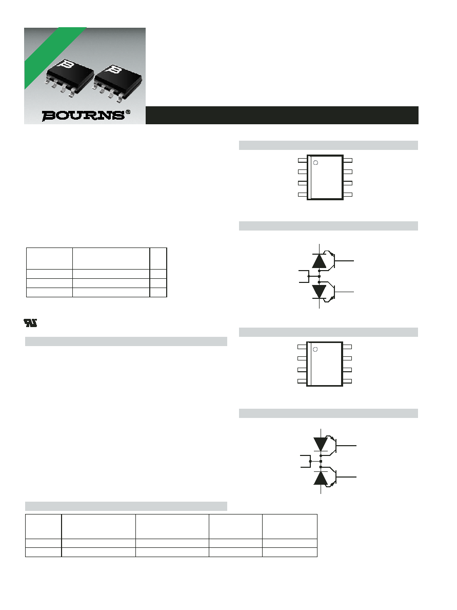
TISP8200M Device Symbol
High Performance Protection for SLICs with +ve & -ve Battery
Supplies
TISP8200M, Negative Overvoltage Protector
≠ Wide 0 to -90 V Programming Range
≠ Low 5 mA max. Gate Triggering Current
≠ High -150 mA min. Holding Current
TISP8201M, Positive Overvoltage Protector
≠ Wide 0 to +90 V Programming Range
≠ Low -5 mA max. Gate Triggering Current
≠ 20 mA min. Holding Current
Rated for International Surge Wave Shapes
How To Order
TISP8200M D Package (Top View)
Description
The TISP8200M/TISP8201M combination has been designed to protect
dual polarity supply rail monolithic SLICs (Subscriber Line Interface
Circuits) against overvoltages on the telephone line caused by lightning,
a.c. power contact and induction. Protection against negative
overvoltages is given by the TISP8200M. Protection against positive
overvoltages is given by the TISP8201M. Both parts are in 8-pin small-
outline surface mount packages.
The TISP8200M has an array of two buffered P-gate SCRs with a
common anode connection. Each SCR cathode and gate has a separate
terminal connection. The NPN buffer transistors reduce the gate supply
current.
In use, the cathodes of the TISP8200M SCRs are connected to the two
conductors of the POTS line (see applications information). The gates are
connected to the appropriate negative voltage battery feed of the SLIC
driving the line conductor pair. This ensures that the TISP8200M
protection voltage tracks the SLIC negative supply voltage. The anode of
the TISP8200M is connected to the SLIC common.
Surface Mount Small-Outline Package
1
2
3
4
5
6
7
8
MDRXAKC
NC - No internal connection
G2
A
A
G1
K1
K2
NC
NC
SDRXAJB
A
A
G1
G2
K1
K2
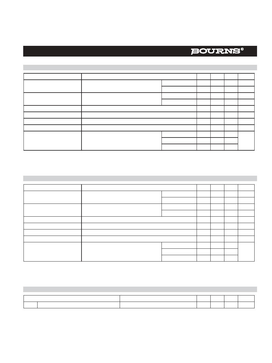
TISP8201M Device Symbol
TISP8201M D Package (Top View)
1
2
3
4
5
6
7
8
MDRXALC
NC - No internal connection
G2
K
K
G1
A1
A2
NC
NC
SDRXAKB
A1
A2
K
K
G1
G2
Wave Shape
Standard
I
tsp
A
2/10
µ
s
Telcordia GR-1089-CORE
210
10/700
µ
s
ITU-T K.20, K.21 & K.45
70
10/1000
µ
s
Telcordia GR-1089-CORE
45
............................................ UL Recognized Components
*RoHS Directive 2002/95/EC Jan 27 2003 including Annex
Device
Package
Carrier
TISP8200M
D (8-pin Small-Outline)
Embossed Tape Reeled
TISP8200MDR
TISP8201M
D (8-pin Small-Outline)
Embossed Tape Reeled
TISP8201MDR
TISP8200MDR-S
TISP8201MDR-S
For Standard
Termination Finish
Order As
For Lead Free
Termination Finish
Order As
*RoHS COMPLIANT
VERSIONS
AVAILABLE

MAY 1998 - REVISED FEBRUARY 2005
Specifications are subject to change without notice.
Customers should verify actual device performance in their specific applications.
Absolute Maximum Ratings for TISP8200M, TA = 25 ∞C (Unless Otherwise Noted)
TISP8200M & TISP8201M
Description (Continued)
Negative overvoltages are initially clipped close to the SLIC negative supply by emitter follower action of the NPN buffer transistor. If sufficient
clipping current flows, the SCR will regenerate and switch into a low voltage on-state condition. As the overvoltage subsides, the high holding
current of the SCR prevents d.c. latchup.
The TISP8201M has an array of two buffered N-gate SCRs with a common cathode connection. Each SCR anode and gate has a separate
terminal connection. The PNP buffer transistors reduce the gate supply current.
In use, the anodes of the TISP8201M SCRs are connected to the two conductors of the POTS line (see applications information). The gates
are connected to the appropriate positive voltage battery feed of the SLIC driving that line pair. This ensures that the TISP8201M protection
voltage tracks the SLIC positive supply voltage. The cathode of the TISP8201M is connected to the SLIC common.
Positive overvoltages are initially clipped close to the SLIC positive supply by emitter follower action of the PNP buffer transistor. If sufficient
clipping current flows, the SCR will regenerate and switch into a low voltage on-state condition. As the overvoltage subsides, the SLIC pulls
the conductor voltage down to its normal negative value and this commutates the conducting SCR into a reverse biassed condition.
Rating
Symbol
Value
Unit
Repetitive peak off-state voltage, TISP8200M V
GK
= 0
V
DRM
-120
V
Repetitive peak reverse voltage, V
GA
= -70 V
V
RRM
120
V
Non-repetitive peak on-state pulse current, (see Notes 1 and 2)
I
TSP
A
10/1000
µ
s (Telcordia/Bellcore GR-1089-CORE, Issue 2, February 1999, Section 4)
-45
5/310
µ
s (ITU-T K.20, K.21& K.45, K.44 open-circuit voltage wave shape 10/700
µ
s)
-70
2/10
µ
s (Telcordia/Bellcore GR-1089-CORE, Issue 2, February 1999, Section 4)
-210
Non-repetitive peak on-state current, 50/60 Hz (see Notes 1, 2 and 3)
I
TSM
A
100 ms
1 s
5 s
300 s
900 s
-11
-6.5
-3.4
-1.4
-1.3
Non-repetitive peak gate current, 2/10
µ
s pulse, cathode commoned (see Note 1)
I
GSM
10
A
Junction temperature
T
J
-55 to +150
∞
C
Storage temperature range
T
stg
-65 to +150
∞
C
NOTES: 1. Initially, the protector must be in thermal equilibrium with -40
∞
C
T
J
85
∞
C. The surge may be repeated after the device returns
to its initial conditions.
2. These non-repetitive rated currents are peak values. The rated current values may be applied to any cathode-anode terminal pair.
Above 85
∞
C, derate linearly to zero at 150
∞
C lead temperature.
3. These non-repetitive rated terminal currents are for the TISP8200M and TISP8201M together. Device (A) terminal positive current
values are conducted by the TISP8201M and (K) terminal negative current values by the TISP8200M.

MAY 1998 - REVISED FEBRUARY 2005
Specifications are subject to change without notice.
Customers should verify actual device performance in their specific applications.
TISP8200M & TISP8201M
Recommended Operating Conditions
Absolute Maximum Ratings for TISP8201M, TA = 25 ∞C (Unless Otherwise Noted)
Rating
Symbol
Value
Unit
Repetitive peak off-state voltage, V
GA
= 0
V
DRM
120
V
Repetitive peak reverse voltage, V
GK
= 70 V
V
RRM
-120
V
Non-repetitive peak on-state pulse current, (see Notes 1 and 2)
I
TSP
A
10/1000
µ
s (Telcordia (Bellcore) GR-1089-CORE, Issue 2, February 1999, Section 4)
45
5/310
µ
s (ITU-T K.20, K.21& K.45, K.44 open-circuit voltage wave shape 10/700
µ
s)
70
2/10
µ
s (Telcordia (Bellcore) GR-1089-CORE, Issue 2, February 1999, Section 4)
210
Non-repetitive peak on-state current, 50/60 Hz (see Notes 1, 2 and 3)
I
TSM
A
100 ms
1 s
5 s
300 s
900 s
11
6.5
3.4
1.4
1.3
Non-repetitive peak gate current, 2/10
µ
s pulse, cathode commoned (see Note 1)
I
GSM
-10
A
Junction temperature
T
J
-55 to +150
∞
C
Storage temperature range
T
stg
-65 to +150
∞
C
NOTES: 1. Initially, the protector must be in thermal equilibrium with -40
∞
C
T
J
85
∞
C. The surge may be repeated after the device returns
to its initial conditions.
2. These non-repetitive rated currents are peak values. The rated current values may be applied to any cathode-anode terminal pair.
Above 85
∞
C, derate linearly to zero at 150
∞
C lead temperature.
3. These non-repetitive rated terminal currents are for the TISP8200M and TISP8201M together. Device (A) terminal positive current
values are conducted by the TISP8201M and (K) terminal negative current values by the TISP8200M.
See Figure 10
Min
Typ
Max
Unit
C1, C2
Gate decoupling capacitor
100
220
nF
R1, R2
Series resistance for Telcordia GR-1089-CORE first-level and second-level surge survival
Series resistance for ITU-T K.20, K.21 and K.45 coordination with a 400 V primary protector
15
10
20
20
MAY 1998 - REVISED FEBRUARY 2005
Specifications are subject to change without notice.
Customers should verify actual device performance in their specific applications.
TISP8200M & TISP8201M
Electrical Characteristics for TISP8200M, TA = 25 ∞C (Unless Otherwise Noted)
Thermal Characteristics
Parameter
Test Conditions
Min
Typ
Max
Unit
I
D
Off-state current
V
D
= V
DRM
, V
GK
= 0
T
J
= 0
∞
C
-5
µ
A
T
J
= 85
∞
C
-50
µ
A
I
R
Reverse current
V
R
= V
RRM
, V
GA
= -70 V
T
J
= 0
∞
C
5
µ
A
T
J
= 85
∞
C
50
µ
A
V
(BO)
Breakover voltage
dv/dt = -250 V/ms, Source Resistance = 300
, V
GA
= -80 V
-82
V
V
(BO)
Breakover voltage
2/10 waveshape, (I
K
) I
T
= -100 A, di/dt
max.
= -58 A/
µ
s, V
GA
= -80 V
-95
V
I
H
Holding current
(I
K
) I
T
= -1 A, di/dt = 1 A/ms, V
GA
= -80 V
-150
mA
I
GT
Gate trigger current
(I
K
) I
T
= -5 A, t
p(g)
20
µ
s, V
GA
= -80 V
5
mA
C
off
Off-state capacitance
f = 1 MHz, V
d
= 1 V, V
GA
= -80 V, (see Note 4)
V
D
= 0
35
pF
V
D
= -5 V
20
V
D
= -50 V
10
NOTE
4: These capacitance measurements employ a three terminal capacitance bridge incorporating a guard circuit. The unmeasured
device terminals are a.c. connected to the guard terminal of the bridge.
Electrical Characteristics for TISP8201M, TA = 25 ∞C (Unless Otherwise Noted)
Parameter
Test Conditions
Min
Typ
Max
Unit
I
D
Off-state current
V
D
= V
DRM
, V
GA
= 0
T
J
= 0
∞
C
5
µ
A
T
J
= 85
∞
C
50
µ
A
I
R
Reverse current
V
R
= V
RRM
, V
GK
= 70 V
T
J
= 0
∞
C
-5
µ
A
T
J
= 85
∞
C
-50
µ
A
V
(BO)
Breakover voltage
dv/dt = 250 V/ms, Source Resistance = 300
, V
GK
= 80 V
82
V
V
(BO)
Breakover voltage
2/10 waveshape, (I
A
) I
T
= 100 A, di/dt
max.
= 58 A/
µ
s, V
GK
= 80 V
95
V
I
H
Holding current
(I
A
) I
T
= 1 A, di/dt = -1 A/ms, V
GK
= 80 V
+20
mA
I
GT
Gate trigger current
(I
A
) I
T
= 5 A, t
p(g)
20
µ
s, V
GK
= 80 V
-5
mA
C
off
Off-state capacitance
f = 1 MHz, V
d
= 1 V, V
GK
= 80 V, (see Note 4)
V
D
= 0
35
pF
V
D
= 5 V
20
V
D
= 50 V
10
NOTE
4: These capacitance measurements employ a three terminal capacitance bridge incorporating a guard circuit. The unmeasured
device terminals are a.c. connected to the guard terminal of the bridge.
Parameter
Test Conditions
Min
Typ
Max
Unit
R
JA
Junction to free air thermal resistance
P
tot
= 0.52 W, T
A
= 70
∞
C, 5 cm
2
, FR4 PCB
160
∞
C/W
MAY 1998 - REVISED FEBRUARY 2005
Specifications are subject to change without notice.
Customers should verify actual device performance in their specific applications.
Parameter Measurement Information
TISP8200M & TISP8201M
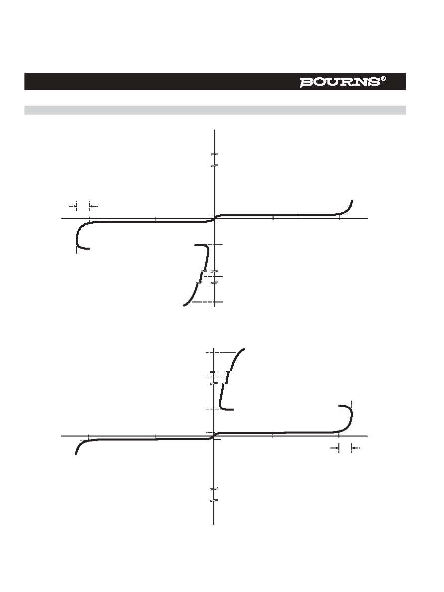
Figure 1. TISP8200M KA Terminal Characteristic
Quadrant I
Blocking
Characteristic
Quadrant III
Switching
Characteristic
+v
-v
V
GA
V
D
I
H
I
TSM
I
TSP
V
(BO)
I
D
+i
-i
V
GK(BO)
V
RRM
V
R
I
R
I
RRM
PM8XACB
Figure 2. TISP8201M AK Terminal Characteristic
-v
V
GK
V
D
V
(BO)
I
H
I
TSM
I
TSP
I
D
Quadrant III
Blocking
Characteristic
+i
-i
Quadrant I
Switching
Characteristic
V
GA(BO)
V
RRM
V
R
I
R
I
RRM
+v
PM8XABB
MAY 1998 - REVISED FEBRUARY 2005
Specifications are subject to change without notice.
Customers should verify actual device performance in their specific applications.
TISP8200M & TISP8201M
APPLICATIONS INFORMATION
Operation of SLICs using Positive and Negative Voltage Supply Rails
Figure 3 shows a typical powering arrangement for a multi-supply rail SLIC. VBATR is a positive supply and VBATL and VBATH are negative
supplies. VBATH is more negative than VBATL. With the positive and negative supply switches S2 and S1 in the positions shown, the line
driver amplifiers are powered between 0 V and VBATL. This mode minimizes the power consumption for short loop transmission. For long
loops, the driver voltage is increased by operating S1 to connect VBATH. To generate ringing, S2 is operated to apply VBATR, powering the
drivers from a total supply voltage of VBATR - VBATH. These conditions are shown in Figure 4.
Figure 4. Driver Supply Voltage Levels
0 V
V
BATL
SHORT LOOP
V
BATH
0 V
LONG LOOP
V
DCRING
V
SLICR
V
PKRING
/2
V
SLICH
V
BATR
AI8XAG
V
BATH
V
V
-
BATR
BATH
RINGING
V
PKRING
/2
V
PKRING
/2
V
PKRING
/2
Conventional ringing is typically unbalanced ground or battery backed. To minimize the supply voltage required, most multi-rail SLICs use
balanced ringing as shown in Figure 4. The ringing has d.c., VDCRING, and a.c., VPKRING, components. A 70 V rms a.c. ring signal has a
peak value, VPKRING, of 99 V. If the d.c. component was 20 V, then the total voltage swing needed would be 99 + 20 = 119 V. There are
internal losses in the SLIC from the positive supply, VSLICR, and the negative supply, VSLICH. The sum of these two losses generally amounts
to a total of 10 V. This makes a total supply rail value of 119 + 10 = 129 V. In practice, the voltage might be distributed as VBATR = +60 V and
VBATH = -70 V. These values are nominal and some extra voltage should be provided to cover power supply voltage tolerance.
Figure 3. SLIC
with Voltage Supply Switching
S1
LINE
DRIVERS
V
BATH
S2
0 V
V
BATR
SLIC
AI8XAF
SUPPLY
SWITCHES
LINE
V
BATL

MAY 1998 - REVISED FEBRUARY 2005
Specifications are subject to change without notice.
Customers should verify actual device performance in their specific applications.
TISP8200M & TISP8201M
SLIC Parameter Values
The table below shows some details of currently available SLICs using positive and negative supply rails.
Manufacturer
INFINEON
LEGERITYTM
Unit
SLIC SERIES
SLIC-S
SLIC-E
ISLICTM
SLIC #
PEB4264
PEB 4265
79R251
Data Sheet Issue
14/07/2000
14/07/2000
-/08/2000
Short Circuit Current
±
130
±
130
±
150
mA
V
BATH
max.
-70
-90
-85
V
V
BATR
max.
+50
+90
+85
V
V
BATR
-V
BATH
max.
90
160
150
V
AC Ringing for:
45
85
65
V rms
V
BATH
-54
-70
-68
V
V
BATR
+36
+80
+52
V
V
BATR
-V
BATH
90
150
120
V
R or T Power Max. < 10 ms
TBA
10
W
R or T Overshoot < 10 ms
-5
5
V
R or T Overshoot < 1 ms
-10
+10
-10
+10
V
R or T Overshoot < 10
µ
s
-10
+30
-10
+30
V
R or T Overshoot < 1
µ
s
-10
10
V
R or T Overshoot < 250 ns
-15
15
V
Line Feed Resistance
20 + 30
20 + 30
50
Legerity, the Legerity logo and ISLIC are the trademarks of Legerity, Inc. (formerly AMD's Communication Products Division).
Other product names used in this publication are for identification purposes only and may be trademarks of their respective
companies.
The maximum total voltage, VBATR - VBATH, is normally about 10 % less than the sum of the maximum VBATR and maximum VBATH values.
In terms of voltage overshoot, ±10 V is needed for 1 µs and ±15 V for 250 ns. It is important to define the protector overshoot under actual
circuit conditions. For example, if the series line feed resistor was 20 , R1 in Figure 10, and Telcordia GR-1089-CORE 2/10 and 10/1000 first
level impulses were applied, the peak protector currents would be 100 A and 33 A. Therefore, the protector voltage overshoot should be
measured at 100 A, 2/10 and 33 A, 10/1000.
Using the table values for maximum battery voltage and minimum overshoot gives a requirement of ±105 V from the output to ground and
±175 V between outputs. There needs to be temperature guard banding for the change in protector characteristics with temperature. To cover
down to -40 ∞C, the 25 ∞C protector minimum values become ±120 V referenced to ground, ±190 V between outputs and 100 V or -100 V on
the gate.
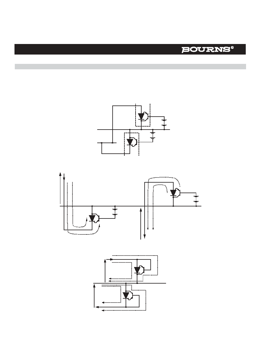
Operation of Gated Protectors
Figure 5 shows how the TISP8200M and TISP8201M limit overvoltages. The TISP8200M SCR sections limit negative overvoltages and the
TISP8201M SCR sections limit positive overvoltages.
The TISP8200M (buffered) gate is connected to the negative SLIC battery feed voltage (VBATH) to provide the protection reference voltage.
Negative overvoltages are initially clipped close to the SLIC negative supply rail value (VBATH) by the conduction of the TISP8200M transistor
base-emitter and the SCR gate-cathode junctions. If sufficient current is available from the overvoltage, then the SCR will crowbar into a low
voltage ground referenced on-state condition. As the overvoltage subsides, the high holding current of the SCR prevents d.c. latchup with the
SLIC output current.
MAY 1998 - REVISED FEBRUARY 2005
Specifications are subject to change without notice.
Customers should verify actual device performance in their specific applications.
TISP8200M & TISP8201M
The negative protection voltage, V(BO), will be the sum of the gate supply (VBATH) and the TISP8200M peak gate(terminal)-cathode voltage
(VGT). Under a.c. overvoltage conditions VGT will be less than 2.0 V. The integrated transistor buffer in the TISP8200M greatly reduces
protector's source and sink current loading on the VBATH supply. Without the transistor, the SCR gate current would charge the VBATH supply.
An electronic power supply is not usually designed to be charged like a battery. As a result, the electronic supply would switch off and the SCR
gate current would provide the SLIC supply current. Normally the SLIC current would be less than the gate current, which would cause the
supply voltage to increase and destroy the SLIC by a supply overvoltage. Older designs using just SCRs needed to incorporate a sacrificial
zener diode across the supply line to go short if the supply voltage increased too much. The integrated transistor buffer removes the charging
problem and the need for a safety zener.
Fast rising impulses will cause short term overshoots in gate-cathode voltage. The negative protection voltage under impulse conditions will
also be increased if there is a long connection between the gate decoupling capacitor, C1, and the gate terminal. During the initial rise of a fast
impulse, the gate current (IG) is the same as the cathode current (IK). Rates of 60 A/µs can cause inductive voltages of 0.6 V in 2.5 cm of
printed wiring track. To minimize this inductive voltage increase of protection voltage, the length of the capacitor to gate terminal tracking
should be minimized.
The TISP8201M (buffered) gate is connected to the positive SLIC battery feed voltage (VBATR) to provide the protection reference voltage.
Positive overvoltages are initially clipped close to the SLIC positive supply rail value (VBATR) by the conduction of the TISP8201M transistor
base-emitter and the SCR gate-anode junctions. If sufficient current is available from the overvoltage, then the SCR will crowbar into a low
voltage ground referenced on-state condition. As the overvoltage subsides the SLIC pulls the conductor voltage down to its normal negative
value and this commutates the conducting SCR into a reverse biassed condition.
Operation of Gated Protectors (Continued)
Voltage Stress Levels on the TISP8200M and TISP8201M
Figure 6 shows the protector electrodes. The package terminal designated gate, G, is the transistor base, B, electrode connection and so is
marked as B (G). The following junctions are subject to voltage stress: Transistor EB and CB, SCR AK (reverse and off state). This clause
covers the necessary testing to ensure the junctions are good.
Testing transistor EB and SCR AK reverse: The highest reverse EB voltage and reverse AK voltage occurs during the overshoot period of the
other protector. For the TISP8200M, the SCR has VBATR plus the TISP8201M overshoot above VBATR. The transistor EB has an additional
VBATH voltage applied (see Figure 7). The reverse current, IR, flowing into the K terminal will be the sum of the transistor IEB and the actual
internal SCR IR . The reverse voltage applied to the K terminal is the TISP8201M protection voltage, V(BO) (VBATR plus overshoot), and the G
terminal has VBATH. Similarly for the TISP8201M, IR is measured with the TISP8200M V(BO) applied and it is the sum of the transistor IEB and
the actual internal SCR IR. VBATR is applied to the G terminal.
Figure 5. Overvoltage Conditions
C1
100 nF
I
G
SLIC
V
BATH
TISP
8200M
I
K
C2
100 nF
V
BATR
0 V
0 V
I
G
I
A
RING
TIP
AI8XAD
TISP
8201M
MAY 1998 - REVISED FEBRUARY 2005
Specifications are subject to change without notice.
Customers should verify actual device performance in their specific applications.
TISP8200M & TISP8201M
Figure 6. Protector Electrodes
V
BATH
TISP
8200M
V
BATR
0 V
AI8XAH
TISP
8201M
0 V
RING
OR
TIP
A
K
E
C
B (G)
A
E
C
B (G)
K
Figure 7. Reverse Current Verification
V
BATH
TISP
8200M
AI8XAJ
0 V
K
B (G)
I
EB
I
R
(internal)
V
BATR
0 V
TISP
8201M
A
B (G)
I
EB
I
R
V
(BO)
8201M
I
R
(internal)
I
R
V
(BO)
8200M
Figure 8. Off-State Current Verification
TISP
8200M
0 V
AI8XAK
T ISP
8201M
0 V
K
B (G)
A
I
CB
I
D
I
CB
V
(BO)
8201M
V
(BO)
8200M
I
D
(internal)
I
D
(internal)
I
D
B (G)
Testing transistor CB and SCR AK off state: The highest AK voltage occurs during the overshoot period of the protector. To make sure that the
SCR blocking junction does not break down during this period, a d.c. test for off-state current can be applied at the overshoot voltage value.
To avoid transistor CB current amplification by the transistor gain, the transistor base-emitter is shorted during this test (see Figure 8).
Summary: Two tests are needed to verify the protector junctions. Maximum current values for IR and ID are required.
Voltage Stress Levels on the TISP8200M and TISP8201M (Continued)
MAY 1998 - REVISED FEBRUARY 2005
Specifications are subject to change without notice.
Customers should verify actual device performance in their specific applications.
TISP8200M & TISP8201M
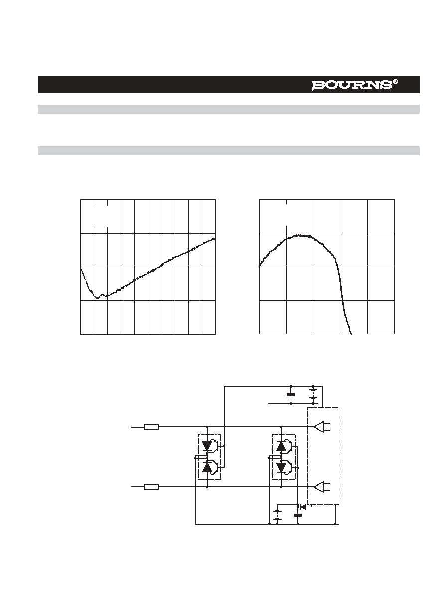
Figure 9. Voltage Overshoot Referenced to Gate Bias Voltage
TISP8200M 2/10 OVERSHOOT
Time - ns
0
100 200 300 400 500 600 700 800 900 1000
O
ver
shoo
t
V
o
l
t
a
g
e
-
V
-20
-10
0
10
20
AI8XAMA
(I
K
) I
T
= -100 A
V
GA
= -80 V
TISP8201M 2/10 OVERSHOOT
Time - ns
0
100
200
300
400
500
O
ver
sh
oo
t
V
o
l
t
a
g
e
- V
-20
-10
0
10
20
AI8XANA
(I
A
) I
T
= +100 A
V
GK
= +80 V
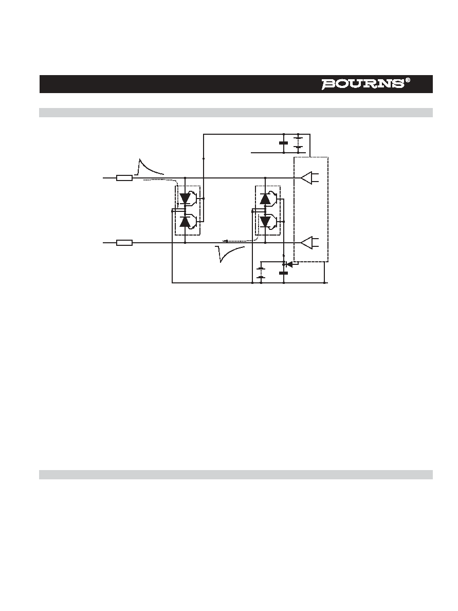
Figure 10. Line Protection with TISP8200M and TISP8201M
C1
100 nF
SLIC
V
BATH
C2
100 nF
V
BATR
0 V
0 V
TISP
8201M
RING
TIP
R1
GR-1089-CORE
R1 = 15
min. (1
st
& 2
nd
level)
ITU-T K.20 & K.21
R1 = 10
min for coordinati on
R1
TISP
8200M
AI8XAE
Figure 9 shows typical overshoots on a 100 A 2/10 waveshape. Both devices are under 10 V peak, which meets the needs of the SLICs listed
earlier.
TISP8200M and TISP8201M Voltage Overshoot
Figure 10 shows a typical circuit for single line protection using one TISP8200M and one TISP8201M. The series resistor values limit the test
impulse currents to within the protector ratings.
Line Protection with TISP8200M and TISP8201M
MAY 1998 - REVISED FEBRUARY 2005
Specifications are subject to change without notice.
Customers should verify actual device performance in their specific applications.
TISP8200M & TISP8201M
MECHANICAL DATA
Device Symbolization Code
Devices are coded as below.
Device
Symbolization
TISP8200M
8200M
TISP8201M
8201M
MAY 1998 - REVISED FEBRUARY 2005
Specifications are subject to change without notice.
Customers should verify actual device performance in their specific applications.
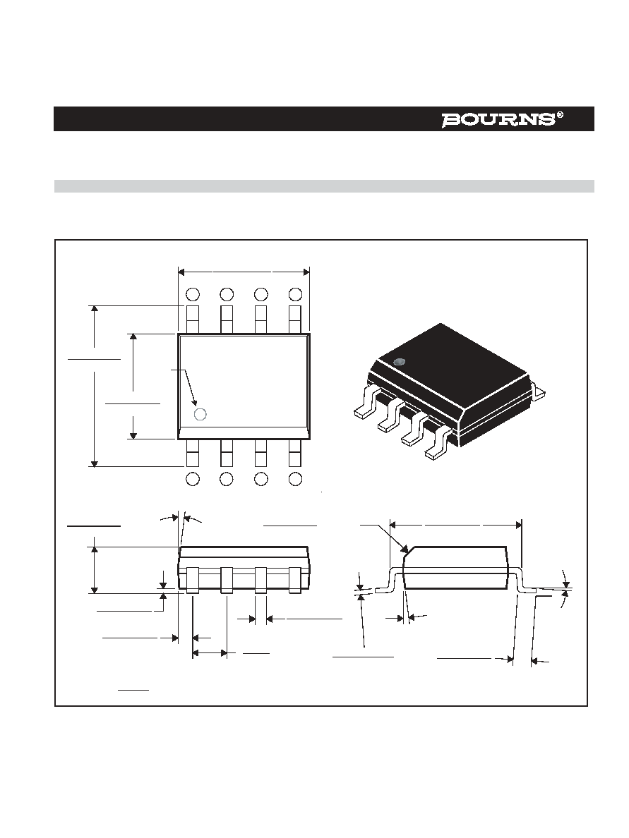
MECHANICAL DATA
D008 Plastic Small Outline Package
This small-outline package consists of a circuit mounted on a lead frame and encapsulated within a plastic compound. The compound will
withstand soldering temperature with no deformation, and circuit performance characteristics will remain stable when operated in high
humidity conditions. Leads require no additional cleaning or processing when used in soldered assembly.
TISP8200M & TISP8201M
NOTES: A. Leads are within 0.25 (0.010) radius of true position at maximum material condition.
B. Body dimensions do not include mold flash or protrusion.
C. Mold flash or protrusion shall not exceed 0.15 (0.006).
D. Lead tips to be planar within
±
0.051 (0.002).
MD XXAAE
5. 80 - 6. 20
(0.228 - 0.244)
4. 80 - 5. 00
(0.189 - 0. 19 7)
D008
8
7
6
5
4
3
2
1
3. 81 - 4. 00
(0.150 - 0.157)
7∞ N O M
3 P la ces
7∞ NOM
4 P la ces
4∞ ± 4∞
0. 28 - 0.79
(0.011 - 0. 03 1)
0. 10 2 - 0.203
(0.004 - 0.008)
8-pin Small Outline Microelectronic Standard
Package MS-012, JEDEC Publication 95
x 45 ∞N O M
0. 19 0 - 0.229
(0.0075 - 0. 00 90)
INDEX
Pin Spacing
1. 27
(0.050)
(see Note A)
6 P laces
1. 35 - 1.75
(0.053 - 0.069)
0. 36 - 0.51
(0.014 - 0.020)
8 P laces
0. 51 - 1.12
(0.020 - 0.044)
0. 25 - 0.50
(0.010 - 0.020)
4. 60 - 5.21
(0.181 - 0.205)
DIMENSIONS ARE:
MILLIMETERS
(INCHES)
MAY 1998 - REVISED FEBRUARY 2005
Specifications are subject to change without notice.
Customers should verify actual device performance in their specific applications.
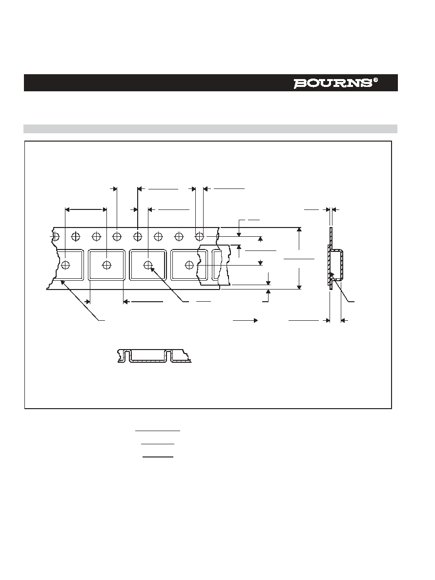
MECHANICAL DATA
TISP8200M & TISP8201M
D008 Tape Dimensions
D008 Package (8-pin Small Outline) Single-Sprocket Tape
7. 90 - 8.10
(.311 - .319)
3. 90 - 4.10
(.154 - .161 )
1. 95 - 2.05
(.077 - .081)
1. 50 - 1.60
(.059 - .063 )
5. 40 - 5.60
(.213 - .220 )
11 .70 - 12.30
(.461 - .484 )
0 MIN .
6. 30 - 6. 50
(.248 - .256)
0. 40
(.016)
2. 0 - 2.2
(.079 - .087 )
Direction of Feed
Carrier Tape
Embossment
Cover
Tape
NOTES: A. Taped devices are supplied on a reel of the following dimensions:-
Reel diameter:
Reel hub diameter:
Reel axial hole:
B. 2500 devices are on a reel.
MDXXATC
MIN .
1. 5
(.059)
MIN .
0. 8
(.0 3)
330 +0.0/- 4.0
(12.99 + 0.0 /-.1 57)
13.0 ±0.2
(.512 ±.008)
10 0 ±2.0
(3.937 ±.079)
"TISP" is a trademark of Bourns, Ltd., a Bourns Company, and is Registered in U.S. Patent and Trademark Office.
"Bourns" is a registered trademark of Bourns, Inc. in the U.S. and other countries.