 | –≠–ª–µ–∫—Ç—Ä–æ–Ω–Ω—ã–π –∫–æ–º–ø–æ–Ω–µ–Ω—Ç: 3656AG | –°–∫–∞—á–∞—Ç—å:  PDF PDF  ZIP ZIP |
Æ
3656
1
3656
Transformer Coupled
ISOLATION AMPLIFIER
FEATURES
q
INTERNAL ISOLATED POWER
q
8000V ISOLATION TEST VOLTAGE
q
0.5
µ
A MAX LEAKAGE AT 120V, 60Hz
q
3-PORT ISOLATION
q
IMR: 125dB REJECTION AT 60Hz
q
1" x 1" x 0.25" CERAMIC PACKAGE
APPLICATIONS
q
MEDICAL
Patient Monitoring and Diagnostic
Instrumentation
q
INDUSTRIAL
Ground Loop Elimination and
Off-ground Signal Measurement
q
NUCLEAR
Input/Output/Power Isolation
This product is covered by the following United States patents: 4,066,974; 4,103,267; 4,082,908. Other patents pending may also apply upon the
allowance and issuance of patents thereon. The product may also be covered in other countries by one or more international patents corresponding
to the above-identified U.S. patents.
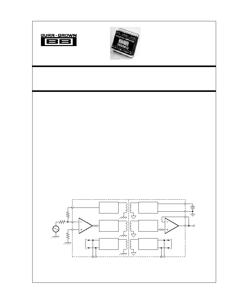
DESCRIPTION
The 3656 was the first amplifier to provide a total
isolation function, both signal and power isolation, in
integrated circuit form. This remarkable advancement
in analog signal processing capability was accom-
plished by use of a patented modulation technique and
miniature hybrid transformer.
Versatility and performance are outstanding features
of the 3656. It is capable of operating with three
completely independent grounds (three-port isolation).
In addition, the isolated power generated is available
to power external circuitry at either the input or
output. The uncommitted op amps at the input and the
output allow a wide variety of closed-loop configura-
tions to match the requirements of many different
types of isolation applications.
Output
Demodulator
Modulator
Pulse
Generator
Input
Demodulator
Rectifiers
and
Filters
Rectifiers
and
Filters
Input
ISO
Power
Output
ISO
Power
+
≠
Æ
©
1987 Burr-Brown Corporation
PDS-403G
Printed in U.S.A. January, 1997
International
Airport
Industrial
Park
∑
Mailing
Address:
PO
Box
11400,
Tucson,
AZ
85734
∑
Street
Address:
6730
S.
Tucson
Blvd.,
Tucson,
AZ
85706
∑
Tel:
(520)
746-1111
∑
Twx:
910-952-1111
Internet:
http://www.burr-brown.com/
∑
FAXLine:
(800)
548-6133
(US/Canada
Only)
∑
Cable:
BBRCORP
∑
Telex:
066-6491
∑
FAX:
(520)
889-1510
∑
Immediate
Product
Info:
(800)
548-6132
SBOS132

Æ
3656
2
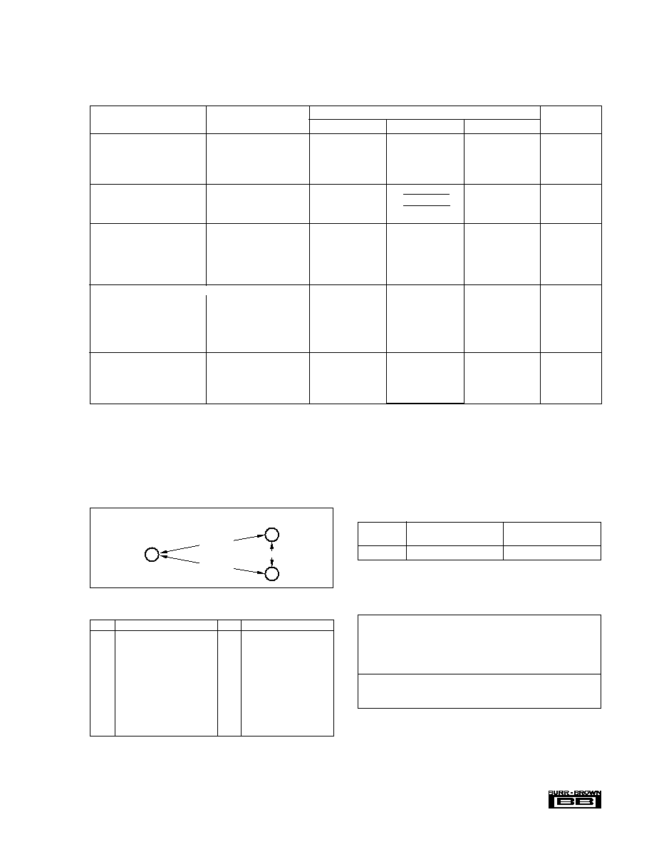
3656AG, BG, HG, JG, KG
PARAMETER
CONDITIONS
MIN
TYP
MAX
UNITS
ISOLATION
Voltage
Rated Continuous
(1)
, DC
3500 (1000)
VDC
Test, 10s
(1)
8000 (3000)
VDC
Test, 60s
(1)
G
1
= 10V/V
2000 (700)
Vrms
Rejection
DC
160
dB
60Hz,
<
100
in I/P Com
(2)
125
dB
60Hz, 5k
in I/P Com
(2)
3656HG
108
dB
3656AG, BG, JG, KG
112
dB
Capacitance
(1)
6 (6.3)
pF
Resistance
(1)
10
12
(10
12
)
Leakage Current
120V, 60Hz
0.28
0.5
µ
A
GAIN
Equations
See Text
Accuracy of Equations
Initial
(3)
3656HG
G
<
100V/V
1.5
%
3656AG, JG, KG
1
%
3656BG
0.3
%
vs Temperature 3656HG
480
ppm/
∞
C
3656AG, JG
120
ppm/
∞
C
3656BG, KG
60
ppm/
∞
C
vs Time
0.02 (1 + log khrs.)
%
Nonlinearity
R
A
+ R
F
= R
B
2M
External Supplies Used at
Pins 12 and 16, 3656HG
Unipolar or Bipolar Output
±
0.15
%
3656AG, JG, KG
±
0.1
%
3656BG
±
0.05
%
Internal Supplies Used for
Bipolar Output Voltage
Output Stage
Swing, Full Load
(4)
±
0.15
%
OFFSET VOLTAGE
(5)
,
RTI
Initial
(3)
, 3656HG
15Vp between P+ and P≠
±
[4 + (40/G
1
)]
mV
3656AG, JG
±
[2 + (20/G
1
)]
mV
3656BG, KG
±
[1 + (10/G
1
)]
mV
vs Temperature, 3656HG
±
[200 + (1000/G
1
)]
µ
V/
∞
C
3656JG
±
[50 + (750/G
1
)]
µ
V/
∞
C
3656AG
±
[25 + (500/G
1
)]
µ
V/
∞
C
3656KG
±
[10 + (350/G
1
)]
µ
V/
∞
C
3656BG
±
[5 + (350/G
1
)]
µ
V/
∞
C
vs Supply Voltage
Supply between P+ and P≠
3656HG
±
[0.6 + (3.5/G
1
)]
mV/V
3656AG, BG, JG, KG
±
[0.3 + (2.1/G
1
)]
mV/V
vs Current
(6)
±
[0.1 + (10/G
1
)]
±
[0.2 + (20/G
1
)]
mV/mA
vs Time
±
[10 + (100/G
1
)] ∑
(1 + log khrs.)
µ
V
AMPLIFIER PARAMETERS, Apply to A
1
and A
2
Bias Current
(7)
Initial
100
nA
vs Temperature
0.5
nA/
∞
C
vs Supply
0.2
nA/V
Offset Current
(7)
5
20
nA
Impedance
Common-Mode
100 || 5
M
|| pF
Input Noise Voltage
f
B
= 0.05Hz to 100Hz
5
µ
Vp-p
f
B
= 10Hz to 10kHz
5
µ
Vrms
Input Voltage Range
(8)
Linear Operation
Internal Supply
±
5
V
External Supply
Supply ≠5
V
Output Current
V
OUT
=
±
5V
±
15V External Supply
±
5
mA
Internal Supply
±
2.5
mA
V
OUT
=
±
10V
±
15V External Supply
±
2.5
mA
V
OUT
=
±
2V, V
P+, P≠
= 8.5V
Internal Supply
±
1
mA
Quiescent Current
150
450
µ
A
SPECIFICATIONS
ELECTRICAL
At +25
∞
C, V
±
= 15VDC and 15VDC between P+ and P≠, unless otherwise specified.
Æ
3656
3
SPECIFICATIONS
(CONT)
ELECTRICAL
At +25
∞
C, V
±
= 15VDC and 15VDC between P+ and P≠, unless otherwise specified.
3656AG, BG, HG, JG, KG
PARAMETER
CONDITIONS
MIN
TYP
MAX
UNITS
FREQUENCY RESPONSE
±
3dB Response
Small Signal
30
kHz
Full Power
1.3
kHz
Slew Rate
Direction Measured at Output
+0.1, ≠0.04
V/
µ
s
Settling Time
to 0.05%
500
µ
s
OUTPUT
Noise Voltage (RTI)
f
B
= 0.05Hz to 100Hz
(
5)
2
+ (22/G
1
)
2
µ
Vp-p
f
B
= 10Hz to 10kHz
(5)
2
+ (11/G
1
)
2
µ
Vrms
Residual Ripple
(9)
5
mVp-p
POWER SUPPLY IN, at P+, P≠
Rated Performance
15
VDC
Voltage Range
(10)
Derated Performance
8.5
16
VDC
Ripple Current
(9)
10
25
mAp-p
Quiescent Current
(11)
Average
14
18
mA/DC
Current vs Load Current
(12)
vs Current from +V, ≠V,
V+, V≠
0.7
mA/mA
ISOLATED POWER OUT, At +V, ≠V,
V+, V≠ pins
(13)
Voltage, No Load
15V Between P+ and P≠
8.5
9
9.5
V
Voltage, Full Load
±
5mA (10mA sum) Load
(12)
7
8
9
V
Voltage vs Power Supply
vs Supply Between P+ and P≠
0.66
V/V
Ripple Voltage
(9)
No Load
40
mVp-p
Full Load
±
5mA Load
80
200
mVp-p
TEMPERATURE RANGE
Specification 3656AG, BG
≠25
+85
∞
C
3656HG, JG, KG
0
+70
∞
C
Operation
(10)
≠55
+100
∞
C
Storage
(14)
≠65
+125
∞
C
NOTES: (1) Ratings in parenthesis are between P- (pin 20) and O/P Com (pin 17). Other isolation ratings are between I/P Com and O/P Com or I/P Com and P≠.
(2) See Performance Curves. (3) May be trimmed to zero. (4) If output swing is unipolar, or if the output is not loaded, specification same as if external supply were used.
(5) Includes effects of A
1
and A
2
offset voltages and bias currents if recommended resistors used. (6) Versus the sum of all external currents drawn from V+, V≠, +V,
≠V (= ISO). (7) Effects of A
1
and A
2
bias currents and offset currents are included in Offset Voltage specifications. (8) With respect to I/P Com (pin 3) for A
1
and with
respect to O/P Com (pin 17) for A
2
. CMR for A
1
and A
2
is 100dB, typical. (9) In configuration of Figure 3. Ripple frequency approximately 750kHz. Measurement bandwidth
is 30kHz. (10) Decreases linearly from 16VDC at 85
∞
C to 12VDC at 100
∞
C. (11) Instantaneous peak current required from pins 19 and 20 at turn-on is 100mA for slow
rising voltages (50ms) and 300mA for fast rises (50
µ
s). (12) Load current is sum drawn form +V, ≠V, V+, V≠ (= I
ISO
). (13) Maximum voltage rating at pins 1 and 4 is
±
18VDC;
maximum voltage rating at pins 12 and 16 is
±
18VDC. (14) Isolation ratings may degrade if exposed to 125
∞
C for more than 1000 hours or 90
∞
C for more than 50,000
hours.
PACKAGE INFORMATION
PACKAGE DRAWING
PRODUCT
PACKAGE
NUMBER
(1)
3656
20-Lead ISO Omni
102A
NOTE: (1) For detailed drawing and dimension table, please see end of data
sheet, or Appendix C of Burr-Brown IC Data Book.
PIN DESIGNATIONS
NO.
DESCRIPTION
NO.
DESCRIPTION
1
+V
11
Output DEMOD
2
MOD Input
12
V≠
3
Input DEMOD COM
13
A
2
Noninverting Input
4
≠V
14
A
2
Inverting Input
5
Balance
15
A
2
Output
6
A
1
Inverting Input
16
V+
7
A
1
Noninverting Input
17
Output DEMOD COM
8
Balance
18
No Pin
9
A
1
Output
19
P+
10
Input DEMOD
20
P≠
ABSOLUTE MAXIMUM RATINGS
Supply Without Damage ...................................................................... 16V
Input Voltage Range Using Internal Supply .........................................
±
8V
Input Voltage Range Using External Supply ................................... Supply
Continuous Isolation Voltage
(1)
..................................... 3500, (1000) VDC
Storage Temperature ...................................................... ≠65
∞
C to +125
∞
C
Lead Temperature, (soldering, 10s) .............................................. +300
∞
C
NOTE: (1) Ratings in parenthesis are between P≠ (pin 20) and O/P Com
(pin 17). Other isolation ratings are between I/P Com and O/P Com or I/P
Com and P≠.
20
17
3
3500VDC
3500VDC
1000VDC
Example of the ratings for 3-port continuous isolation.

Æ
3656
4
TYPICAL PERFORMANCE CURVES
All specifications typical at +25
∞
C, unless otherwise specified.
≠30
Frequency (Hz)
SMALL SIGNAL FREQUENCY RESPONSE
Relative Gain (dB)
5
0
≠5
≠10
≠15
≠20
≠25
1k
100
100k
3k
30k
G
1
= 100
G
1
= 1000
G
1
= 1
V
P
= 15V
V+, V≠ = +15V, ≠15V
V
OUT
= 300mVrms
G
2
= 2
G
1
= 10
300
10k
3
Power Supply Voltage P± (V)
OUTPUT SWING vs SUPPLY VOLTAGE
Output Voltage (±V)
11
9
7
5
10
14
8
16
12
1 (±V) = 5mA
G
2
= 2 (±V) = ±5mA
R
L
= 3k
, ext. V± = ±15V
R
L
= 2k
, int. V± or
R
L
= 1k
, ext. V± = ±15V
1 (±V) = 0
0
Frequency (Hz)
OUTPUT SWING AND DISTORTION vs FREQUENCY
Output Voltage (±V)
7
6
5
4
3
2
1
100
10
10k
1k
0
7
6
5
4
3
2
1
G = 100
G = 1000
G = 1
Output Swing
Distortion
G = 10
Harmonic Distortion (%)
50k
Phase Shift (∞C)
30
0
30
60
90
120
150
180
210
240
270
G
1
= 100
G
1
= 1000
G
1
= 1
V
P
= 15V
V+, V≠ = +15V, ≠15
V
OUT
= 300mVrms
G
1
= 10
Frequency (Hz)
PHASE RESPONSE
1k
100
100k
10k
1
Temperature (∞C)
OUTPUT VOLTAGE SWING vs TEMPERATURE
AND ISOLATED SUPPLY LOAD
Output Voltage (±V)
9
7
5
3
0
85
≠75
100
50
I
ISO
= 0, ≠V
OUT
I
ISO
(see note 12 of electrical specs)
I
ISO
= 0, +V
OUT
R
B
= 2M
I
ISO
= max, ≠V
OUT
I
ISO
= max, +V
OUT
Derated Vp±
≠50
25
75
≠25
≠55
10
NOISE VOLTAGE vs FREQUENCY
Noise Voltage (nV/ Hz)
0.1
10k
100
Frequency (Hz)
10k
1k
100
Output Stage
1k
10
1
100k
Input Stage

Æ
3656
5
TYPICAL PERFORMANCE CURVES
(CONT)
All specifications typical at +25
∞
C, unless otherwise specified.
0.6
QUIESCENT CURRENT vs TEMPERATURE
Normalized Quiescent Current (at V
P+P≠
)
2.2
1.8
1.4
1
Derated Vp±
Temperature (∞C)
0
85
≠75
100
50
≠50
25
75
≠25
≠55
0
ISOLATED OUTPUT VOLTAGE AND CURRENT
vs TEMPERATURE
Maximum Recommended I
ISO
Current (±mA)
8
6
4
2
Isolated Voltage Output (±V)
0
16
12
8
4
±V at I
ISO
= 0
Voltage
Current
±V at I
ISO
= max
Derated Vp±
Temperature (∞C)
0
85
≠75
100
50
≠50
25
75
≠25
≠55
7
Supply Voltage at V
P±
(V)
QUIESCENT CURRENT AND ISOLATED VOLTAGE
OUTPUT vs SUPPLY VOLTAGE
Quiescent Current at V
p+p≠
(mA)
15
13
11
9
10
14
8
16
12
Isolated Voltage Output (±V)
2
10
8
6
4
Voltage at I
ISO
= 0
Voltage at I
ISO
= ±5mA
Current
60
Gain (V/V)
ISOLATION-MODE REJECTION vs GAIN
Isolation-Mode Rejection (dB)
200
180
160
140
120
100
80
10
1
1000
100
R
C
is resistance in series
with input common, pin 3.
Shielded
Unshielded
f = 60Hz
R
C
= 0
R
C
= 5k
≠50
Frequency (Hz)
ISOLATION MODE REJECTION
vs FREQUENCY
Normalized Isolation Mode
Rejection (dB)
100k
100
1k
10
10k
20
10
0
≠10
≠20
≠30
≠40
0
Isolation Voltage (Vp)
AC AND DC LEAKAGE CURRENT
vs ISOLATION VOLTAGE
AC Leakage Current (µA)
50
40
30
20
10
2k
8k
0
10k
4k
6k
0
2.5
2
1.5
1
0.5
DC Leakage Current (nA)
DC
AC, 60Hz

Æ
3656
6
THEORY OF OPERATION
Details of the 3656 are shown in Figure 1. The external
connections shown, place it in its simplest gain configura-
tion --unity gain, noninverting. Several other amplifier gain
configurations and power isolation configurations are
possible. See Installation and Operating Instructions and
Applications sections for details.
Isolation of both signal and power is accomplished with a
single miniature toroid transformer with multiple windings.
A pulse generator operating at approximately 750kHz pro-
vides a two-part voltage waveform to transformer, T
1
. One
part of the waveform is rectified by diodes D
1
through D
4
to
provide the isolated power to the input and output stages
(+V, ≠V and V+, V≠). The other part of the waveform is
modulated with input signal information by the modulator
operating into the V
2
winding of the transformer.
The modulated signal is coupled by windings W
6
and W
7
to
two matched demodulators--one in the input stage and one
in the output stage--which generate identical voltages at
their outputs, pins 10 and 11 (Voltages identical with respect
to their respective commons, pins 3 and 17). In the input
stage the input amplifier, A
1
, the modulator and the input
demodulator are connected in a negative feedback loop. This
forces the voltage at pin 6 (connect as shown in Figure 1) to
equal the input signal voltage applied at pin 7. Since the
input and the output demodulators are matched and produce
identical output voltages, the voltage at pin 11 (referenced to
pin 17, the output common) is equal to the voltage at pin 10
(referenced to pin 3, the input common). In the output stage,
output amplifier A
2
is connected as a unity gain buffer, thus
the output voltage at pin 15 equals the output demodulator
voltage at pin 11. The end result is an isolated output voltage
FIGURE 1. Block Diagram.
at pin 15 equal to the input voltage at pin 7 with no galvanic
connection between them.
Several amplifier and power connection variations are pos-
sible:
1. The input stage may be connected in various operational
amplifier gain configurations.
2. The output stage may be operated at gains above unity.
3. The internally generated isolated voltages which provide
power to A
1
and A
2
may be overridden and external
supply voltages used instead.
Versatility and its three independent isolated grounds allow
simple solutions to demanding analog signal conditioning
problems. See the Installation and Operating Instructions
and Applications sections for details.
INSTALLATION AND
OPERATING INSTRUCTIONS
The 3656 is a very versatile device capable of being used in
a variety of isolation and amplification configurations. There
are several fundamental considerations that determine con-
figuration and component value constraints:
1. Consideration must be given to the load placed on the
resistance (pin 10 and pin 11) by external circuitry. Their
output resistance is 100k
and a load resistor of 2M
or
greater is recommended to prevent a voltage divider
loading effect in excess of 5%.
Output
Demodulator
Modulator
Pulse
Generator
Input
Demodulator
9
2
7
6
1
5
10
W
6
W
2
W
4
D
3
D
1
V
IN
+
≠
T
1
W
1
W
7
W
3
19
P+
20
P≠
0.47µF
15VDC
+
≠
100k
100k
11
14
13
15
16
V+
D
2
W
5
0.47µF
12
V≠
D
4
17
≠
+
BAL
BAL
3
+V
A
2
A
1
8
4
≠V
0.47µF
V
OUT

Æ
3656
7
2. Demodulator loadings should be closely matched so their
output voltages will be equal. (Unequal demodulator
output voltages will produce a gain error.) At the 2M
level, a matching error of 5% will cause an additional
gain error of 0.25%.
3. Voltage swings at demodulator outputs should be limited
to 5V. The output may be distorted if this limit is
exceeded. This constrains the maximum allowed gains of
the input and output stages. Note that the voltage swings
at demodulator outputs are tested with 2M
load for a
minimum of 5V.
4. Total current drawn from the internal isolated supplies
must be limited to less than
±
5mA per supply and limited
to a total of 10mA. In other words, the combination of
external and internal current drawn from the internal
circuitry which feeds the +V, ≠V, V+ and V≠ pins should
be limited to 5mA per supply (total current to +V, ≠V, V+
and V≠ limited to 10mA). The internal filter capacitors
for
±
V are 0.01
µ
F. If more than 0.1mA is drawn to
provide isolated power for external circuitry (see Figure
12), additional capacitors are required to provide ad-
equate filtering. A minimum of 0.1
µ
F/mA is recom-
mended.
5. The input voltage at pin 7 (noninverting input to A
1
) must
not exceed the voltage at pin 4 (negative supply voltage
for A
1
) in order to prevent a possible lockup condition. A
low leakage diode connected between pins 7 and 4, as
shown in Figure 2, can be used to limit this input voltage
swing.
6. Impedances seen by each amplifier's + and ≠ input
terminals should be matched to minimize offset voltages
caused by amplifier input bias currents. Since the de-
modulators have a 100k
output resistance, the amplifier
input not connected to the demodulator should also see
100k
.
7. All external filter capacitors should be mounted as close
to the respective supply pins as possible in order to
prevent excessive ripple voltages on the supplies or at the
output. (Optimum spacing is less than 0.5". Ceramic
capacitors recommended.)
POWER AND
SIGNAL CONFIGURATIONS
NOTE: Figures 2, 3 and 4 are used to illustrate both signal
and power connection configurations. In the circuits shown,
the power and signal configurations are independent so that
any power configuration could be used with any signal
configuration.
ISOLATED POWER CONFIGURATIONS
The 3656 is designed with isolation between the input, the
output, and the power connections. The internally generated
isolated voltages supplied to A
1
and A
2
may be overridden
with external voltages greater than the internal supply volt-
ages. These two features of 3656 provide a great deal of
versatility in possible isolation and power supply hook-ups.
When external supplies are applied, the rectifying diodes
(D
1
through D
4
) are reverse biased and the internal voltage
sources are decoupled from the amplifiers (see Figure 1).
Note that when external supplies are used, they must never
be lower than the internal supply voltage.
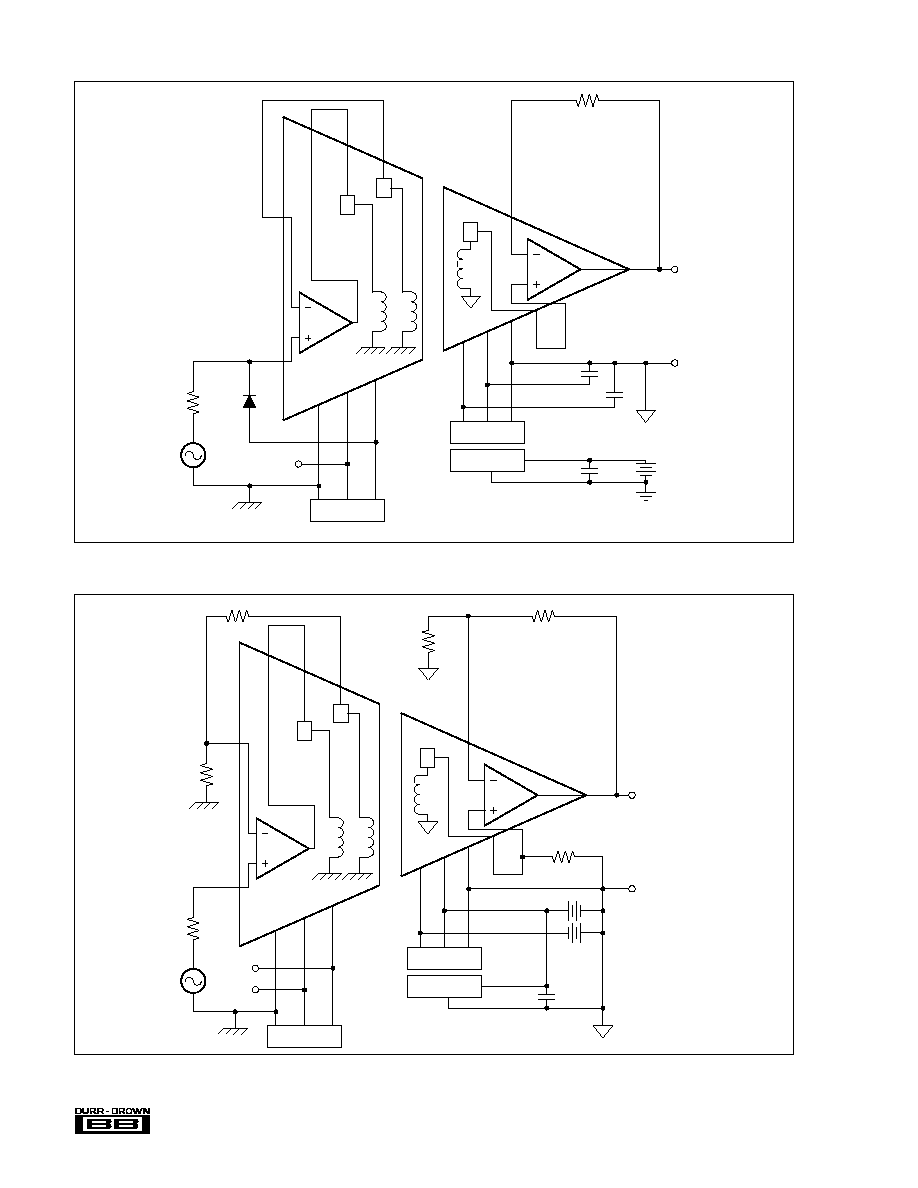
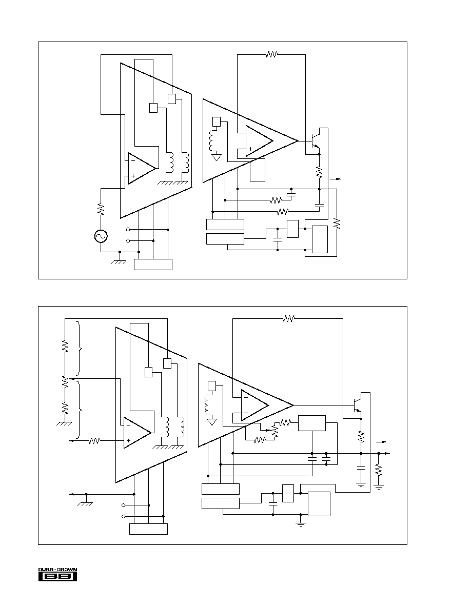
Three-Port
The power supply connections in Figure 2 show the full
three-port isolation configuration. The system has three
separate grounds with no galvanic connections between
them. The two external 0.47
µ
F capacitors at pins 12 and 16
filter the rectified isolated voltage at the output stage. Filter-
ing on the input stage is provided by internal capacitors. In
this configuration continuous isolation voltage ratings are:
3500V between pins 3 and 17; 3500V between pins 3 and
19; 1000V between pins 17 and 19.
Two-Port Bipolar Supply
Figure 3 shows two-port isolation which uses an external
bipolar supply with its common connected to the output
stage ground (pin 17). One of the supplies (either + or ≠
could be used) provides power to the pulse generator (pins
19 and 20). The same sort of configuration is possible with
the external supplies connected to the input stage. With the
connection shown, filtering at pins 12 and 16 is not required.
In this configuration continuous isolation voltage rating is:
3500VDC between pins 3 and 17; not applicable between
pins 17 and 19; 3500VDC between pins 3 and 19.
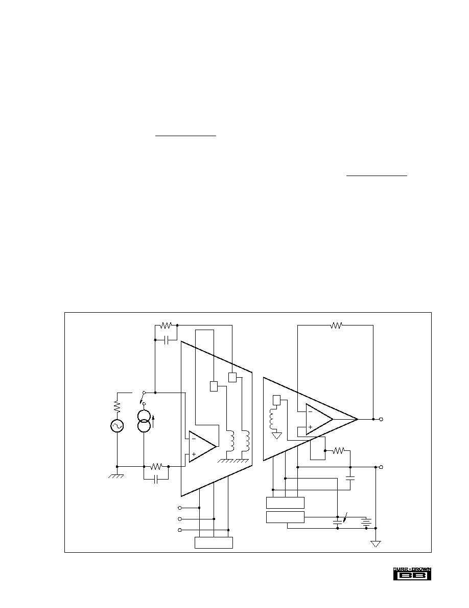
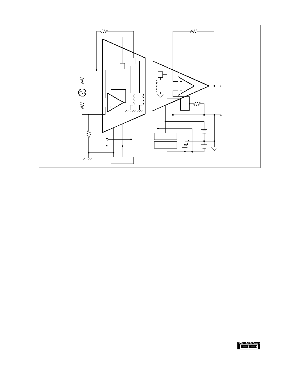
Two-Port Single Supply
Figure 4 demonstrates two-port isolation using a single
polarity supply connected to the output common (pin 17).
The other polarity of supply for A
2
is internally generated
(thus the filtering at pin 12). This isolated power configura-
tion could be used at the input stage as well and either
polarity of supply could be employed. In this configuration
continuous isolation voltage rating is: 3500V between pins
3 and 17; 3500V between pins 3 and 19; not applicable
between pins 17 and 19.
SIGNAL CONFIGURATIONS
Unity Gain Noninverting
The signal path portion of Figure 2 shows the 3656 is its
simplest gain configuration: unity gain noninverting. The
two 100k
resistors provide balanced resistances to the
inverting and noninverting inputs of the amplifiers. The
diode prevents latch up in case the input voltage goes more
negative than the voltage at pin 4.
Noninverting With Gain
The signal path portion of Figure 3 demonstrates two addi-
tional gain configurations: gain in the output stage and
noninverting gain in the input stage. The following equa-
tions apply:
Æ
3656
8
FIGURE 2. Power: Three-Port Isolation; Signal: Unity-Gain Noninverting.
FIGURE 3. Power: Two-Port, Dual Supply; Signal: Noninverting Gain.
D
D
M
V
IN
+
≠
R
C
100k
I/P PWR
100k
+
≠
0.47µF
≠
+
15V
V
OUT
7
4
6
9
2
10
15
11
13
17
16
12
O/P PWR
Pulse GEN
19
1
3
20
14
0.47µF
0.47µF
A
1
A
2
D
D
M
V
IN
+
≠
R
C
I/P PWR
R
X
+
≠
0.47µF
≠
+
19
20
R
F
R
A
+
≠
V
OUT
R
B
R
K
7
4
6
9
2
10
15
11
13
17
16
12
O/P PWR
Pulse GEN
1
3
14
15V
15V
A
1
A
2
Æ
3656
9
Total amplifier gain:
G = G
1
∑ G
2
= V
OUT
V
IN
Input Stage:
G
1
= 1 + (R
A
/F
A
)
(Select G
1
to be less than 5V/full scale V
IN
to limit
demodulator output to 5V).
R
A
+ R
F
2M
(Select to load input demodulator with at least 2M
).
R
C
= R
A
|| (R
F
+ 100k
) =
(Balance impedances seen by the + and ≠ inputs
of A
1
to reduce input offset caused by bias current).
Output Stage:
G
2
= 1 + (R
X
/R
K
)
(Select ratio to obtain V
OUT
between 5V and 10V
full scale with V
IN
at its maximum).
R
X
|| R
K
= 100k
(Balance impedances seen by the + and ≠ inputs
of A
2
to reduce effect of bias current on the
output offset).
R
B
= R
A
+ R
F
(Load output demodulator equal to input demodulator).
Inverting Gain, Voltage or Current Input
The signal portion of Figure 4 shows two possible inverting
input stage configurations: current and input, and voltage
input.
Input Stage:
For the voltage input case:
G
1
= ≠R
F
/R
S
(Select G
1
to be less than 5V/full scale V
IN
to limit the demodulator output voltage to 5V).
R
F
= 2M
(Select to load the demodulator with
at least 2M
).
R
C
= R
S
|| (R
1
+ 100k
) =
(Balance the impedances seen by the + and≠ inputs of A
1
).
For the current input case:
V
OUT
= ≠I
IN
R
F
∑ G
2
R
C
= R
F
R
F
may be made larger than 2M
if desired. The 10pF
capacitors are used to compensate for the input capacitance
of A
1
and to insure frequency stability.
Output Stage:
The output stage is the same as shown in equations (5), (6),
and (7).
(1)
(2)
(3)
(11)
(12)
(8)
FIGURE 4. Power: Two-Port, Single Supply; Signal: Inverting Gains.
(4)
R
A
(R
F
+ 100k
)
R
A
+ R
F
+ 100k
(5)
(6)
(7)
(9)
R
S
(R
F
+ 100k
)
R
S
+ R
F
+ 100k
(10)
D
D
M
I/P PWR
100k
+
≠
0.47µF
0.47µF
≠
+
19
20
10pF
R
F
= 2M
R
B
= 2M
V
IN
+
≠
R
S
10pF
R
C
I
IN
V
OUT
7
4
6
9
2
10
15
11
13
17
16
12
O/P PWR
Pulse GEN
1
3
14
A
2
A
1

Æ
3656
10
Illustrative Calculations:
The maximum input voltage is 100mV. It is desired to
amplify the input signal for maximum accuracy. Noninverting
output is desired.
Input Stage:
Step 1
G
1
max = 5V/max Input Signal = 5V 0.1V = 50V/V
With the above gain of 50V/V, if the input ever exceeds
100mV, it would drive the output to saturation. Therefore, it
is good practice to allow reasonable input overrange.
So, to allow for 25% input overrange without saturation at
the output, select:
G
1
= 40V/V
G
1
= 1 + (R
F
+ R
A
) = 40
R
F
+ R
A
= 39
(13)
Step 2
R
A
+ R
F
forms a voltage divider with the 100k
output
resistance of the demodulator. To limit the voltage divider
loading effect to no more than 5%, R
A
+ R
F
should be
chosen to be at least 2M
. For most applications, the 2M
should be sufficiently large for R
A
+ R
F
. Resistances greater
than 2M
may help decrease the loading effect, but would
increase the offset voltage drift.
The voltage divider with R
A
+ R
F
= 2M
is 2M
/(2M
+
100k
) = 2/(2 + 0.1) = 95.2%, i.e., the percent loading is
4.8%.
Choose R
A
+ R
F
= 2M
(14)
Step 3
Solving equations (13) and (14)
R
A
= 50k
and R
F
= 1.95M
Step 4
The resistances seen by the + and ≠ input terminals of the
input amplifier A
1
should be closely matched in order to
minimize offset voltage due to bias currents.
R
C
= R
A
|| (R
F
+ 100k
)
= 50k
|| (1.95M
+ 100k
)
49k
Output Stage:
Step 5
V
OUT
= V
IN MAX
∑ G
1
∑ G
2
As discussed in Step 1, it is good practice to provide 25%
input overrange.
So we will calculate G
2
for 10V output and 125% of the
maximum input voltage.
V
OUT
= (1.25 ∑ 0.1)(G
1
)(G
2
)
i.e., 10V = 0.125 ∑ 40 ∑ G
2
G
2
= 10V/5V = 2V/V
Step 6
G
2
= 1 + (R
X
/R
K
) = 2.0
R
X
/R
K
= 1.0
R
X
= R
K
(15)
Step 7
The resistance seen by the + input terminal of the output
stage amplifier A
2
(pin 13) is the output resistance 100k
of
the output demodulator. The resistance seen by the (≠) input
terminal of A
2
(pin 14) should be matched to the resistance
seen by the + input terminal.
The resistance seen by pin 14 is the parallel combination of
R
X
and R
K
.
R
X
|| R
K
= 100k
(R
X
∑ R
K
/(R
X
+ R
K
) = 100k
R
K
/[1 +(R
K
/R
X
)] = 100k
(16)
Step 8
Solving equations (15) and (16) R
K
= 20k
and R
X
=
200k
.
Step 9
The output demodulator must be loaded equal to the input
demodulator.
R
B
= R
A
+ R
F
= 2M
(See equation (14) above in Step 2).
Use the resistor values obtained in Steps 3, 4, 8 and 9, and
connect the 3656 as shown in Figure 3.
OFFSET TRIMMING
Figure 5 shows an optional offset voltage trim circuit. It is
important that R
A
+ R
F
= R
B
.
CASE 1: Input and output stages in low gain, use output
potentiometer (R
2
) only. Input potentiometer (R
1
)
may be disconnected. For example, unity gain
could be obtained by setting R
A
= R
B
= 20M
, R
C
= 100k
, R
F
= 0, R
X
= 100k
, and R
K
=
.
CASE 2: Input stage in high gain and output stage in low
gain, use input potentiometer (R
1
) only. Output
potentiometer (R
2
) may be disconnected. For
example, G
T
= 100 could be obtained by setting
R
F
= 2M
, R
B
= 2M
returned to pin 17, R
A
=
20k
, R
X
= 100k
, and R
K
=
.
CASE 3: When it is necessary to perform a two-stage
precision trim (to maintain a very small offset
change under conditions of changing temperature
and changing gain in A
1
and A
2
), use step 1 to
adjust the input stage and step 2 for the output
stage. Carbon composition resistors are accept-
able, but potentiometers should be stable.
Step 1: Input stage trim (R
A
= R
C
= 20k
, R
I
= R
B
= 20M
.
R
X
= 100k
, R
K
=
, R
2
disconnected); A
1
high, A
2
low gain. Adjust R
1
for 0V
±
5mV or desired setting
at V
OUT
, pin 15.

Æ
3656
11
Step 2: Output stage trim (R
A
= R
B
= 20M
, R
C
= 100k
,
R
F
= 0, R
X
= 100k
, R
K
=
, R
1
and R
2
connected);
A
1
low, A
2
low gain. Adjust R
2
for 0V
±
1mV or
desired setting at V
OUT
, pin 15 (
±
110mV approxi-
mate total range).
NOTE: Other circuit component values can be used with
valid results.
APPLICATIONS
ECG AMPLIFIER
Although the features of the circuit shown in Figure 6 are
important in patient monitoring applications, they may also
be useful in other applications. The input circuitry uses an
external, low quiescent current op amp (OPA177 type)
powered by the isolated power of the input stage to form a
high impedance instrumentation amplifier input (true three-
wire input). R
3
and R
4
give the input stage amplifier of the
3656 a noninverting gain of 10 and an inverting gain of ≠9.
R
1
and R
2
give the external amplifier a noninverting gain of
1 + 1/9. The inputs are applied to the noninverting inputs of
the two amplifiers and the composite input stage amplifier
has a gain of 10.
The 330k
, 1W, carbon resistors and diodes D
1
- D
4
provide
protection for the input amplifiers from defibrillation pulses.
The output stage in Figure 6 is configured to provide a
bandpass filter with a gain of 22.7 (68M
/3M
). The high-
pass section (0.05Hz cutoff) is formed by the 1
µ
F capacitor
and 3M
resistor which are connected in series between the
output demodulator and the inverting input of the output
stage amplifier. The low-pass section (100Hz cutoff) is
formed by the 68M
resistor and 22pF capacitor located in
the feedback loop of the output stage. The diodes provide for
quick recovery of the high-pass filter to overvoltages at the
input. The 100k
pot and the 100M
resistor allow the
output voltage to be trimmed to compensate for increased
offset voltage caused by unbalanced impedances seen by the
inputs of the output stage amplifier.
In many modern electrocardiographic systems, the patient is
not grounded. Instead, the right-leg electrode is connected to
the output of an auxiliary operational amplifier as shown in
Figure 7. In this circuit, the common-mode voltage on the
body is sensed by the two averaging resistors, R
1
and R
2
,
inverted, amplified, and fed back to the right-leg through
resistor R
4
. This negative feedback drives the common-
mode voltage to a low value. The body's displacement
current i
d
does not flow to ground, but rather to the output
circuit of A
3
. This reduces the pickup as far as the ECG
amplifier is concerned and effectively grounds the patient.
The value of R
4
should be as large as practical to isolate the
patient from ground. The resistors R
3
and R
4
may be se-
lected by these equations:
R
3
= (R
1
/2) (V
O
/V
CM
) and R
4
= (V
CM
≠ V
O
)/i
d
(≠10V
V
O
+10V and ≠10V
V
CM
+10V)
D
D
M
R
C
I/P PWR
R
X
+
≠
0.47µF
≠
+
19
20
R
F
R
A
V
OUT
R
B
R
K
R
1
100k
R
2
100k
+
≠
15V
15V
7
4
6
9
2
10
15
11
13
17
16
12
O/P PWR
Pulse GEN
1
3
14
8
5
A
1
A
2
FIGURE 5. Optional Offset Voltage Trim.

Æ
3656
12
FIGURE 7. Driven Right-Leg Amplifier.
FIGURE 6. ECG Amplifier.
330k
R
A
D
3
D
4
+V
≠V
D
D
M
7
4
3M
6
9
2
10
15
16
19
11
12
High
Out
Low
Out
0.1µF
≠
+
15VDC
1
24V
0.5W
300k
330k
L
A
1/2
OPA1013
D
1
3
14
3656
13
17
20
3M
0.1µF
D
2
3M
100k
R
1
20k
R
2
20k
270k
+V
≠V
+V
≠V
+V
≠V
OPA177
+V
≠V
R
3
R
4
i
d
D
1
= D
2
= D
3
= D
4
= 1N459
+V
≠V
1/2
OPA1013
V
O
A
1
A
2
1µF
D
D
M
7
4
I/P PWR
6
9
2
10
15
68M
(1)
11
13
17
16
12
High
Low
0.47µF
(3)
O/P PWR
Pulse GEN
0.47µF
≠
+
15VDC
19
1N4148s
3M
22pF
100k
100M
(4)
1
24V
0.5W
R
4
330k
R
1
11k
(2)
330k
1W
R
2
100k
L
A
330k
1W
R
A
R
L
OPA177
D
1
D
3
D
2
D
4
NOTES: (1) Bandpass 0.05Hz to 100Hz. (2) Adjustable resistor may be used to achieve max common-mode
rejection between L
A
/R
A
and RL.(3) Negative 15V supply may be connected in place of 0.47µF capacitor if available.
(4) See offset trimming section.
3
20
14
1N4148s 300k
R
3
3M
A
2
A
1

Æ
3656
13
FIGURE 8. Bipolar Current Output.
where V
O
is the output voltage of A
3
, and V
CM
is the
common-mode voltage between the inputs L
A
and R
A
and
the input common at pin 3 of the 3656.
This circuit has the added benefit of having higher common-
mode rejection than the circuit in Figure 6 (approximately
10dB improvement).
BIPOLAR CURRENT OUTPUT
The three-port capability of the 3656 can be used to imple-
ment a current output isolation amplifier function--usually
difficult to implement when grounded loads are involved.
The circuit is shown in Figure 8 and the following equations
apply:
G = I
OUT
/V
IN
= 1 +
X
I
OUT
±
2.5mA
V
1
±
4V (compliance)
R
L
1.6k
R
F
+ R
A
= R
1
+ R
2
2M
CURRENT OUTPUT--
LARGER UNIPOLAR CURRENTS
A more practical version of the current output function is
shown in Figure 9. If the circuit is powered from a source
greater than 15V as shown, a three-terminal regulator should
R
A
R
F
be used to provide 15V for the pulse generator (pins 19 and
20). The input stage is configured as a unity gain buffer,
although other configurations such as current input could be
used. The circuit uses the isolation feature between the
output stage and the primary power supply to generate the
output current configuration that can work into a grounded
load. Note that the output transistors can only drive positive
current into the load. Bipolar current output
would require a
second transistor and dual supply.
ISOLATED 4mA TO 20mA OUTPUT
Figure 10 shows the circuit of an expanded version of the
isolated current output function. It allows any input voltage
range to generate the 4mA to 20mA output excursion and is
also capable of zero suppression. The "span" (gain) is
adjusted by R
2
and the "zero" (4mA output for minimum
input) is set by the 200k
pot in the output stage. A three-
terminal 5V reference is used to provide a stable 4mA
operating point. The reference is connected to insert an
adjustable bias between the demodulator output and the
noninverting input of the output stage.
DIFFERENTIAL INPUT
Figure 11 shows the proper connections for differential input
configuration. The 3656 is capable of operating in this input
configuration only for floating loads (i.e., the source V
IN
has no connection to the ground reference established at
pin 3). For this configuration the usual 2M
resistor used in
(R
1
+ R
2
) ∑ R
S
R
2
R
A
D
D
M
V
IN
+
≠
R
C
I/P PWR
+
≠
0.47µF
0.47µF
≠
+
15V
V
L
7
4
6
9
2
10
15
11
13
17
16
12
O/P PWR
Pulse GEN
19
1
3
20
14
R
F
R
L
R
1
R
2
R
S
0.47µF
I
OUT
A
1
A
2
Æ
3656
14
FIGURE 9. Isolated 1 to 5V
IN
/ 4mA to 20mA I
OUT
.
FIGURE 10. Isolated 4mA to 20mA I
OUT
.
D
D
M
V
IN
+
≠
100k
I/P PWR
0.47µF
≠
+
7
4
6
9
2
10
15
11
13
17
16
12
O/P PWR
Pulse GEN
19
1
3
20
14
0.47µF
I
OUT
100k
250
10
0.47µF
R
L
10
15V
24V
Supply
A
1
A
2
D
D
M
I/P PWR
0.47µF
≠
+
7
4
6
9
2
10
15
11
13
17
16
12
O/P PWR
Pulse GEN
19
1
3
20
14
0.47µF
I
OUT
400k
200
R
L
15V
24V
Supply
R
3
R
C
R
2
R
1
R
F
R
A
V
IN
+
≠
1.5M
200k
200k
REF02
5V
0.47µF
Ripple
Filter
2N2219A
A
1
A
2
Æ
3656
15
FIGURE 11. Differential Input, Floating Source.
the input stage is split into two halves, R
F
and R
F≠
. The
demodulator load (seen by pin 10 with respect to pin 3) is
still 2M
for the floating load as shown. Notice pin 19 is
common in Figure 11 whereas pin 20 is common in previous
figures.
SERIES STRING SOURCE
Figure 12 shows a situation where a small voltage, which is
part of a series string of other voltages, must be measured.
The basic problem is that the small voltage to be measured
is 500V above the system ground (i.e., a system common-
mode voltage of 500V exists). The circuit converts this
system CMV to an amplifier isolation mode voltage. Thus,
the isolation voltage ratings and isolation-mode rejection
specifications apply.
IMPROVED INPUT CHARACTERISTICS
In situations where it is desired to have better DC input
amplifier characteristics than the 3656 normally provides, it
is possible to add a precision operational amplifier as shown
in Figure 13. Here the instrumentation grade OPA177 is
supplied from the isolated power of the input stage. The
3656 is configured as a unity-gain buffer. The gain of the
OPA177 stage must be chosen to limit its full scale output
voltage to 5V and avoid overdriving the 3656's demodula-
tors. Since the 3656 draws a significant amount of supply
current, extra filtering or the input supply is required as
shown (2
x
0.47
µ
F).
ELECTROMAGNETIC RADIATION
The transformer coupling used in 3656 for isolation makes
the 3656 a source of electromagnetic radiation unless it is
properly shielded. Physical separation between the 3656 and
sensitive components may not give sufficient attenuation by
itself. In these applications, the use of an electromagnetic
shield is a must. A shield, Burr-Brown 100MS, is specially
designed for use with the 3656 package. Note that the offset
voltage appearing at pin 15 may change by 4mV to 12mV
with use of the shield; however, this can be trimmed (see
Offset Trimming section).
The information provided herein is believed to be reliable; however, BURR-BROWN assumes no responsibility for inaccuracies or omissions. BURR-BROWN
assumes no responsibility for the use of this information, and all use of such information shall be entirely at the user's own risk. Prices and specifications are subject
to change without notice. No patent rights or licenses to any of the circuits described herein are implied or granted to any third party. BURR-BROWN does not
authorize or warrant any BURR-BROWN product for use in life support devices and/or systems.
D
D
M
R
F
1M
I/P PWR
100k
+
≠
0.47µF
≠
+
15V
V
OUT
7
4
6
9
2
10
15
11
13
17
16
12
O/P PWR
Pulse GEN
19
1
3
20
14
V
IN
+
≠
R
1
R
1
R
F
1M
2M
≠
+
15V
V
OUT
= ≠V
IN
(R
F
/R
1
) R
F
= R
1
A
2
A
1

Æ
3656
16
FIGURE 12. Series Source.
FIGURE 13. Isolator for Low-Level Signals.
D
D
M
I/P PWR
100k
+
0.47µF
≠
+
15V
V
OUT
7
4
9
2
10
15
11
13
17
16
12
O/P PWR
Pulse GEN
19
1
3
20
14
V
S
R
F
2M
≠
+
15V
V
OUT
= [V
IN
( 500V/1MR)] [ 1 + (R
F
/R
A
)] R
A
+ R
F
= 2M
≠
V
IN
=
500mV
+
≠
R
A
6
R
C
1000V
R
S
=
10
500V
500V
A
1
A
2
D
100k
+
≠
0.47µF
≠
+
15V
V
OUT
15
11
17
16
12
O/P PWR
Pulse GEN
19
20
14
≠
+
15V
V
OUT
= [1 + (R
1
/R
2
)] V
IN
D
M
7
4
I/P PWR
6
9
2
10
1
R
1
V
IN
OPA177
3
13
0.47µF
0.47µF
R
2
+
≠
A
1
A
2

IMPORTANT NOTICE
Texas Instruments and its subsidiaries (TI) reserve the right to make changes to their products or to discontinue
any product or service without notice, and advise customers to obtain the latest version of relevant information
to verify, before placing orders, that information being relied on is current and complete. All products are sold
subject to the terms and conditions of sale supplied at the time of order acknowledgment, including those
pertaining to warranty, patent infringement, and limitation of liability.
TI warrants performance of its semiconductor products to the specifications applicable at the time of sale in
accordance with TI's standard warranty. Testing and other quality control techniques are utilized to the extent
TI deems necessary to support this warranty. Specific testing of all parameters of each device is not necessarily
performed, except those mandated by government requirements.
Customers are responsible for their applications using TI components.
In order to minimize risks associated with the customer's applications, adequate design and operating
safeguards must be provided by the customer to minimize inherent or procedural hazards.
TI assumes no liability for applications assistance or customer product design. TI does not warrant or represent
that any license, either express or implied, is granted under any patent right, copyright, mask work right, or other
intellectual property right of TI covering or relating to any combination, machine, or process in which such
semiconductor products or services might be or are used. TI's publication of information regarding any third
party's products or services does not constitute TI's approval, warranty or endorsement thereof.
Copyright
©
2000, Texas Instruments Incorporated