
FEATURES
D
20-Bit Effective Resolution
D
High-Impedance Buffered Input
D
±
2.5V Differential Input Range
D
Pin-Compatible with ADS1244
D
0.0006% INL (typ), 0.0015% INL (max)
D
Simple Two-Wire Serial Interface
D
Simultaneous 50Hz and 60Hz Rejection
D
Single Conversions with Sleep Mode
D
Single-Cycle Settling
D
Self-Calibration
D
Well Suited for Multi-Channel Systems
D
Easily Connects to the MSP430
D
Current Consumption: 158
µ
A
D
Analog Supply: 2.5V to 5.25V
D
Digital Supply: 1.8V to 3.6V
APPLICATIONS
D
Hand-Held Instrumentation
D
Portable Medical Equipment
D
Industrial Process Control
D
Test and Measurement Systems
DESCRIPTION
The ADS1245 is a 24-bit, delta-sigma analog-to-digital
converter (ADC). It offers excellent performance and very
low power in an MSOP-10 package and is well suited for
demanding high-resolution measurements, especially in
portable and other space- and power-constrained
systems.
The buffered input presents an impedance of 3G
, mini-
mizing measurement errors when using high-impedance
sources. The ADS1245 is compatible with ADS1244 and
offers a direct upgrade path for designs requiring higher in-
put impedance.
A third-order delta-sigma (
) modulator and digital filter
form the basis of the ADC. The analog modulator has a
±
2.5V differential input range. The digital filter rejects both
50Hz and 60Hz signals, completely settles in one cycle,
and outputs data at 15 samples per second (SPS).
A simple, two-wire serial interface provides all the
necessary control. Data retrieval, self-calibration, and
Sleep mode are handled with a few simple waveforms.
When only single conversions are needed, the ADS1245
can be shut down (Sleep mode) while idle between
measurements to dramatically reduce the overall power
dissipation. Multiple ADS1245s can be connected
together to create a synchronously sampling multichannel
measurement system. The ADS1245 is designed to easily
connect to microcontrollers, such as the MSP430.
The ADS1245 supports 2.5V to 5.25V analog supplies and
1.8V to 3.6V digital supplies. Power is typically less than
470
µ
W in normal operation and less than 1
µ
W during
Sleep mode.
Digital
Filter
Serial
Interface
DRDY/DOUT
SCLK
CLK
AINN
AINP
VREFP VREFN
AVDD
GND
DVDD
3rd-Order
Modulator
Buffer
All trademarks are the property of their respective owners.
PRODUCTION DATA information is current as of publication date. Products
conform to specifications per the terms of Texas Instruments standard warranty.
Production processing does not necessarily include testing of all parameters.
SBAS287A - JUNE 2003 - REVISED SEPTEMBER 2003
Low-Power, 24-Bit
Analog-to-Digital Converter
ADS1245
www.ti.com
Copyright
2003, Texas Instruments Incorporated
Please be aware that an important notice concerning availability, standard warranty, and use in critical applications of Texas Instruments
semiconductor products and disclaimers thereto appears at the end of this data sheet.

ADS1245
SBAS287A - JUNE 2003 - REVISED SEPTEMBER 2003
www.ti.com
2
ORDERING INFORMATION
PRODUCT
PACKAGE-LEAD
PACKAGE
DESIGNATOR(1)
SPECIFIED
TEMPERATURE
RANGE
PACKAGE
MARKING
ORDERING
NUMBER
TRANSPORT
MEDIA, QUANTITY
ADS1245
MSOP-10
DGS
-40
∞
C to +85
∞
C
BHI
ADS1245IDGST
Tape and Reel, 250
ADS1245
MSOP-10
DGS
-40
∞
C to +85
∞
C
BHI
ADS1245IDGSR
Tape and Reel, 2500
(1) For the most current specifications and package information, refer to our web site at www.ti.com.
ABSOLUTE MAXIMUM RATINGS
over operating free-air temperature range unless otherwise noted(1)
ADS1245
UNIT
AVDD to GND
-0.3 to +6
V
DVDD to GND
-0.3 to +3.6
V
Input Current
100, momentary
mA
Input Current
10, continuous
mA
Analog Input Voltage to GND
-0.5 to AVDD + 0.5
V
Analog Input Voltage to GND
-0.3 to DVDD + 0.3
V
Digital Output Voltage to GND
-0.3 to DVDD + 0.3
V
Maximum Junction Temperature
+150
∞
C
Operating Temperature Range
-40 to +85
∞
C
Storage Temperature Range
-60 to +150
∞
C
Lead Temperature (soldering, 10s)
+300
∞
C
(1) Stresses above these ratings may cause permanent damage.
Exposure to absolute maximum conditions for extended periods
may degrade device reliability. These are stress ratings only, and
functional operation of the device at these or any other conditions
beyond those specified is not implied.
This integrated circuit can be damaged by ESD. Texas
Instruments recommends that all integrated circuits be
handled with appropriate precautions. Failure to observe
proper handling and installation procedures can cause damage.
ESD damage can range from subtle performance degradation to
complete device failure. Precision integrated circuits may be more
susceptible to damage because very small parametric changes could
cause the device not to meet its published specifications.
PIN ASSIGNMENTS
DGS PACKAGE
MSOP
(TOP VIEW)
1
2
3
4
5
10
9
8
7
6
CLK
SCLK
DRDY/DOUT
DVDD
AVDD
GND
VREFP
VREFN
AINN
AINP
ADS1245
Terminal Functions
TERMINAL
NAME
NO.
DESCRIPTION
GND
1
Analog and digital ground
VREFP
2
Positive reference input
VREFN
3
Negative reference input
AINN
4
Negative analog input
AINP
5
Positive analog input
AVDD
6
Analog power supply, 2.5V to 5.25V
DVDD
7
Digital power supply, 1.8V to 3.6V
DRDY/DOUT
8
Dual-purpose output:
Data ready: indicates valid data by going low.
Data output: outputs data, MSB first, on the
first rising edge of SCLK.
SCLK
9
Serial clock input: clocks out data on the
rising edge. Used to initiate calibration and
Sleep mode (see text for more details).
CLK
10
System clock input: typically 2.4576MHz

ADS1245
SBAS287A - JUNE 2003 - REVISED SEPTEMBER 2003
www.ti.com
3
ELECTRICAL CHARACTERISTICS
All specifications at TA = -40
∞
C to +85
∞
C, AVDD = +5V, DVDD = +3V, fCLK = 2.4576MHz, and VREF = +1.25V, unless otherwise noted.
PARAMETER
TEST CONDITIONS
MIN
TYP
MAX
UNIT
Analog Input
Full-scale input voltage range
AINP - AINN
±
2VREF
V
Absolute input range
AINP, AINN with respect to GND
GND + 0.1
AVDD - 1.25
V
Differential input impedance
fCLK = 2.4576MHz
3
G
System Performance
Resolution
No missing codes
24
Bits
Data rate
fCLK = 2.4576MHz
15
SPS(1)
Integral nonlinearity (INL)
Differential input signal, end point fit
±
0.0006
±
0.0015
%FSR
(2)
Offset error
1
14
ppm of FSR
Offset error drift(3)
0.01
ppm of FSR/
∞
C
Gain error(4)
0.005
0.1
%
Gain error drift(3)
0.5
ppm/
∞
C
At DC
90
100
dB
Common-mode rejection
fCM(5) = 50
±
1Hz, fCLK = 2.4576MHz
100
dB
Common-mode rejection
fCM = 60
±
1Hz, fCLK = 2.4576MHz
100
dB
Normal-mode rejection
fSIG(6) = 50
±
1Hz, fCLK = 2.4576MHz
60
dB
Normal-mode rejection
fSIG = 60
±
1Hz, fCLK = 2.4576MHz
70
dB
Input referred noise
2
ppm of FSR,
RMS
Analog power-supply rejection
At DC,
AVDD = 5%
100
dB
Digital power-supply rejection
At DC,
AVDD = 5%
100
dB
Voltage Reference Input
Reference input voltage (VREF)
VREF
VREFP - VREFN
0.5
1.25
AVDD(7)
V
Negative reference input (VREFN)
GND - 0.1
VREFP - 0.5
V
Positive reference input (VREFP)
VREFN + 0.5
AVDD + 0.1
V
Voltage reference impedance
fCLK = 2.4576MHz
1
M
Digital Input/Output
VIH (CLK, SCLK)
0.8 DVDD
5.25
V
Logic levels
VIL (CLK, SCLK)
GND
0.2 DVDD
V
Logic levels
VOH (DRDY, DOUT)
IOH = 1mA
DVDD - 0.4
DVDD
V
VOL (DRDY, DOUT)
IOL = 1mA
GND
DVDD + 0.4
V
Input leakage (CLK, SCLK)
0 < (CLK, SCLK) < DVDD
±
10
µ
A
CLK frequency (fCLK)
6
MHz
CLK duty cycle
30
70
%
Power Supply
AVDD
2.7
5.25
V
DVDD
1.8
3.6
V
Sleep mode
0.1
1
µ
A
AVDD current
AVDD = 3V
152
µ
A
AVDD current
AVDD = 5V
158
250
µ
A
Sleep mode, CLK stopped
0.1
µ
A
DVDD current
Sleep mode, 2.4576MHZ CLK running
1.6
5
µ
A
DVDD current
DVDD = 3V
5
10
µ
A
Total power dissipation
AVDD = DVDD = 3V
0.47
mW
(1) SPS = samples per second.
(2) FSR = full-scale range = 4VREF.
(3) Recalibration can reduce these errors to the level of the noise.
(4) Achieving specified gain error performance requires that calibration be performed with reference voltage input between (GND + 0.1V) and
(AVDD - 1.25V). See Voltage Reference Inputs section.
(5) fCM is the frequency of the common-mode input.
(6) fSIG is the frequency of the input signal.
(7) It will not be possible to reach the digital output full-scale code when VIN > 2VREF.

ADS1245
SBAS287A - JUNE 2003 - REVISED SEPTEMBER 2003
www.ti.com
4
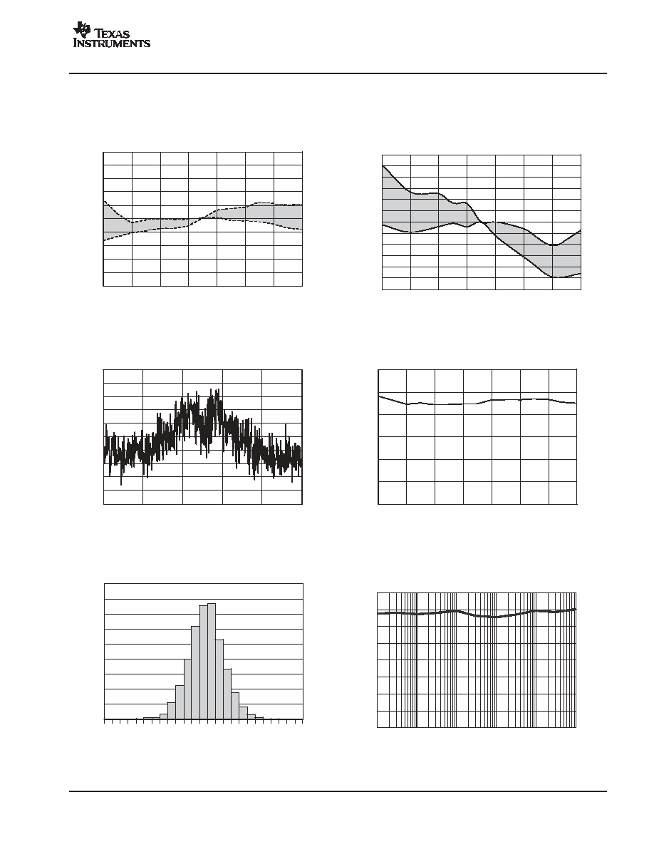
TYPICAL CHARACTERISTICS
At TA = +25
∞
C, AVDD = +5V, DVDD = +3V, fCLK = 2.4576MHz, and VREF = +1.25V, unless otherwise specified.
Figure 1
ANALOG CURRENT vs TEMPERATURE
Temperature (
_
C)
C
u
r
r
ent
(
µ
A)
15
-
5
-
25
35
55
75
95
-
45
220
210
200
190
180
170
160
150
140
130
120
110
100
AVDD = +3V, f
CLK
= 2.4576MHz
AVDD = +5V, f
CLK
= 4.9152MHz
Figure 2
DIGITAL CURRENT vs TEMPERATURE
Temperature (
_
C)
Cu
r
r
e
n
t
(
µ
A)
15
-
5
-
25
35
55
75
95
-
45
12
10
8
6
4
2
0
DVDD = +1.8V, f
CLK
= 2.4576MHz
DVDD = +3V, f
CLK
= 4.9152MHz
Figure 3
ANALOG CURRENT vs ANALOG SUPPLY
Analog Supply (V)
C
u
rre
n
t
(
µ
A)
4.0
3.5
3.0
4.5
5.0
5.5
2.5
164
162
160
158
156
154
152
150
148
f
CLK
= 2.4576MHz
f
CLK
= 4.9152Hz
Figure 4
DIGITAL CURRENT vs DIGITAL SUPPLY
Digital Supply (V)
Cu
r
r
e
n
t
(
µ
A)
15
-
5
-
25
35
55
75
95
-
45
16
14
12
10
8
6
4
2
0
f
CLK
= 4.9152MHz
f
CLK
= 2.4576MHz
Figure 5
INTEGRAL NONLINEARITY vs ANALOG SUPPLY
V
REF
= 1.25; f
OSC
= 2.4576MHz
V
CM
= 2.4 or ((
1.8)/2 + 0.3), whichever is smaller
(V)
INL
(
p
p
m
o
f
F
SR)
4.0
3.5
3.0
4.5
5.0
5.5
2.5
30
25
20
15
10
5
0
T = +25
_
C
T = +85
_
C
T =
40
_
C
-
-
AVDD
AVDD
Figure 6
INTEGRAL NONLINEARITY vs V
IN
V
IN
(V)
T = +25
_
C
T = +85
_
C
T =
-
40
_
C
INL
(
p
p
m
o
f
F
S
R
)
-
1.5
-
0.5
0.5
1.5
2.5
-
2.5
12.5
10.0
7.5
5.0
2.5
0
-
2.5
-
5.0
-
7.5
-
10.0
-
12.5
ADS1245
SBAS287A - JUNE 2003 - REVISED SEPTEMBER 2003
www.ti.com
5
TYPICAL CHARACTERISTICS
At TA = +25
∞
C, AVDD = +5V, DVDD = +3V, fCLK = 2.4576MHz, and VREF = +1.25V, unless otherwise specified.
Figure 7
OFFSET vs TEMPERATURE
Temperature (
_
C)
N
o
r
m
al
i
z
ed
O
f
f
s
et
(
p
pm
of
F
S
R
)
15
-
5
-
25
35
55
75
95
-
45
5
4
3
2
1
0
-
1
-
2
-
3
-
4
-
5
GAIN vs TEMPERATURE
Temperature (
_
C)
G
a
in
(
N
o
r
m
a
li
ze
d
)
15
-
5
-
25
35
55
75
95
-
45
1.00006
1.00005
1.00004
1.00003
1.00002
1.00001
1.00000
0.99999
0.99998
0.99997
0.99996
0.99995
0.99994
Figure 8
Figure 9
NOISE vs INPUT SIGNAL
V
IN
(V)
No
i
s
e
(
p
p
m
o
f
F
S
R
,
R
M
S
)
-
1.5
-
0.5
0.5
1.5
2.5
-
2.5
3.2
3.0
2.8
2.6
2.4
2.2
2.0
1.8
1.6
1.4
1.2
Figure 10
NOISE vs TEMPERATURE
Temperature (
_
C)
No
i
s
e
(
p
p
m
o
f
F
S
R,
RM
S
)
15
-
5
-
25
35
55
75
95
-
45
3.0
2.5
2.0
1.5
1.0
0.5
0
Figure 11
HISTOGRAM OF OUTPUT DATA
ppm of FSR
N
u
m
b
er
o
f
O
c
c
u
r
e
n
c
es
-
14
-
12
-
10
-
9
-
8
-
7
-
6
-
5
-
4
-
3
-
2
-
1
0
1
2
3
4
5
6
7
8
9
10
11
12
900
800
700
600
500
400
300
200
100
0
Figure 12
COMMON-MODE REJECTION RATIO
vs FREQUENCY
Frequency (Hz)
CM
RR
(
d
B
)
1k
100
10
10k
100k
1
160
140
120
100
80
60
40
20
0