 | –≠–ª–µ–∫—Ç—Ä–æ–Ω–Ω—ã–π –∫–æ–º–ø–æ–Ω–µ–Ω—Ç: ADS5220 | –°–∫–∞—á–∞—Ç—å:  PDF PDF  ZIP ZIP |

ADS5220
12-Bit, 40MSPS Sampling, +3.3V
ANALOG-TO-DIGITAL CONVERTER
FEATURES
q
HIGH SNR: 70dB
q
HIGH SFDR: 88dBFS
q
LOW POWER: 195mW
q
INTERNAL/EXTERNAL REFERENCE OPTION
q
SINGLE-ENDED OR
FULLY DIFFERENTIAL ANALOG INPUT
q
PROGRAMMABLE INPUT RANGE
q
LOW DNL: 0.3LSB
q
SINGLE +3.3V SUPPLY OPERATION
q
TQFP-48 PACKAGE
APPLICATIONS
q
WIRELESS LOCAL LOOP
q
COMMUNICATIONS
q
MEDICAL IMAGING
q
PORTABLE INSTRUMENTATION
DESCRIPTION
The ADS5220 is a pipeline, CMOS Analog-to-Digital Con-
verter (ADC) that operates from a single +3.3V power
supply. This converter can be operated with a single-ended
input or differential input. The ADS5220 includes a 12-bit
quantizer, high bandwidth track-and-hold, and an internal
reference. It also allows the user to disable the internal
reference and utilize external references which provide ex-
cellent gain and offset matching when used in multi-channel
applications or in applications where full-scale range adjust-
ment is required.
The ADS5220 employs digital error correction techniques to
provide excellent differential linearity for demanding imag-
ing applications. Its low distortion and high SNR give the
extra margin needed for medical imaging, communications,
video, and test instrumentation. The ADS5220 offers power
dissipation of 195mW and also provides two power-down
modes.
The ADS5220 is specified at a maximum sampling fre-
quency of 40MSPS and a differential input range of
1V to 2V. The ADS5220 is available in a TQFP-48 package.
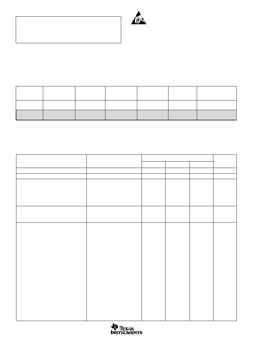
ADS5220
SBAS261A ≠ APRIL 2003 ≠ REVISED MARCH 2004
12-Bit
Pipelined
ADC
Internal
Reference
Timing/Duty Cycle
Adjust
Circuitry
Error
Correction
Logic
3-State
Output
S/H
CLK
VDRV
ADS5220
AV
DD
OE
RSEL
REFB
REFT
OVR
QPD
STPD
D0
D11
∑
∑
∑
VREF
IN
V
IN
IN
www.ti.com
PRODUCTION DATA information is current as of publication date.
Products conform to specifications per the terms of Texas Instruments
standard warranty. Production processing does not necessarily include
testing of all parameters.
Copyright © 2003-2004, Texas Instruments Incorporated
Please be aware that an important notice concerning availability, standard warranty, and use in critical applications of
Texas Instruments semiconductor products and disclaimers thereto appears at the end of this data sheet.
All trademarks are the property of their respective owners.
ADS5220
2
SBAS261A
www.ti.com
SPECIFIED
PACKAGE
TEMPERATURE
PACKAGE
ORDERING
TRANSPORT
PRODUCT
PACKAGE-LEAD
DESIGNATOR
(1)
RANGE
MARKING
NUMBER
MEDIA, QUANTITY
ADS5220
TQFP-48
PFB
≠40
∞
C to +85
∞
C
ADS5220PFB
ADS5220PFBT
Tape and Reel, 250
"
"
"
"
"
ADS5220IPFBR
Tape and Reel, 2000
ADS5220
QFN-48
(2)
RGZ
≠40
∞
C to +85
∞
C
ADS5220RGZ
ADS5220RGZ
Rails, 52
"
"
"
"
"
ADS5220IRGZR
Tape and Reel, 1000
NOTE: (1) For the most current specifications and package information, refer to our web site at www.ti.com.
(2) This package available Q2 2004.
ADS5220
PARAMETER
CONDITIONS
MIN
TYP
MAX
UNITS
ELECTROSTATIC
DISCHARGE SENSITIVITY
This integrated circuit can be damaged by ESD. Texas Instru-
ments recommends that all integrated circuits be handled with
appropriate precautions. Failure to observe proper handling
and installation procedures can cause damage.
ESD damage can range from subtle performance degradation
to complete device failure. Precision integrated circuits may be
more susceptible to damage because very small parametric
changes could cause the device not to meet its published
specifications.
AV
DD
, DV
DD
, VDRV ........................................................................... +3.8V
Analog Input ............................................................. ≠0.3V to (+V
S
+ 0.3V)
Logic Input ............................................................... ≠0.3V to (+V
S
+ 0.3V)
Case Temperature ......................................................................... +100
∞
C
Junction Temperature .................................................................... +150
∞
C
Storage Temperature ..................................................................... +150
∞
C
NOTE: (1) Stresses above these ratings may cause permanent damage.
Exposure to absolute maximum conditions for extended periods may degrade
device reliability.
ABSOLUTE MAXIMUM RATINGS
(1)
PACKAGE/ORDERING INFORMATION
ELECTRICAL CHARACTERISTICS: AV
DD
= 3.3V
T
MIN
= ≠40
∞
C, T
MAX
= +85
∞
C, typical values are at T
A
= +25
∞
C, sampling rate = 40MSPS, 50% clock duty cycle, AV
DD
= 3.3V, DV
DD
= 3.3, VDRV = 2.5V, ≠1dBFS, DCA
off, internal reference voltage, and 2V
PP
differential input, unless otherwise noted.
RESOLUTION
12 Tested
Bits
SPECIFIED TEMPERATURE RANGE
Ambient Air
≠40 to +85
∞
C
ANALOG INPUT
Single-Ended Input Range
2V
PP
0.5
2.5
V
Optional Single-Ended Input Range
1V
PP
1
2
V
Differential Input Range
2V
PP
1
2
V
Analog Input Bias Current
1
µ
A
Input Impedance
Static, No Clock
1.25 || 5
M
|| pF
Analog Input Bandwidth
≠3dBFS Input
300
MHz
CONVERSION CHARACTERISTICS
Sample Rate
1M
40M
Samples/s
Data Latency
5
Clock Cycle
Clock Duty Cycle
Mode Select Enabled
35 to 65
%
DYNAMIC CHARACTERISTICS
Differential Linearity Error (largest code error)
f = 2.4MHz
±
0.3
±
0.75
LSB
f = 9.7MHz
±
0.35
LSB
No Missing Codes
Tested
Integral Nonlinearity Error, f = 2.4MHz
±
0.7
±
1.5
LSBs
Spurious-Free Dynamic Range
(1)
Referred to Full-Scale
f = 2.4MHz
88
dBFS
(2)
f = 9.7MHz
83
88
dBFS
f = 19.8MHz
76
dBFS
2-Tone Intermodulation Distortion
(3)
f = 9.5MHz and 10.5MHz (≠7dB each tone)
86.3
dBc
Signal-to-Noise Ratio (SNR)
Referred to Full-Scale
f = 2.4MHz
70
dBFS
f = 9.7MHz
68.5
70
dBFS
f = 19.8MHz
69
dBFS
Signal-to-(Noise + Distortion) (SINAD)
Referred to Full-Scale
f = 2.4MHz
69
dBFS
f = 9.7MHz
68
69
dBFS
f = 19.8MHz
68
dBFS
Effective Number of Bits
(4)
, f = 2.4MHz
11.2
Bits
Output Noise
Input Tied to Common-Mode
0.3
LSBrms
Aperture Delay Time
3
ns
Aperture Jitter
1.2
ps rms
Over-Voltage Recovery Time
1.0
Clock Cycle
Full-Scale Step Acquisition Time
5
ns
ADS5220
3
SBAS261A
www.ti.com
DIGITAL INPUTS
Logic Family
Convert Command
Start Conversion
High Level Input Current
(5)
(V
IN
= 3V
DD
)
100
µ
A
Low Level Input Current (V
IN
= 0V)
10
µ
A
High Level Input Voltage
+1.7
V
Low Level Input Voltage
+0.7
V
Input Capacitance
5
pF
DIGITAL OUTPUTS
Logic Family
Logic Coding
Low Output Voltage (I
OL
= 50
µ
A to 1.5mA)
VDRV = 2.5V
+0.1
V
High Output Voltage (I
OH
= 50
µ
A to 0.5mA)
+2.4
V
3-State Enable Time
OE = H
20
40
ns
3-State Disable Time
OE = L
2
10
ns
Output Capacitance
5
pF
ACCURACY (Internal Reference, 2V
PP
,
unless otherwise noted)
Zero Error (referred to midscale)
f
IN
= 2.4MHz, at 25
∞
C
±
0.75
±
1.5
%FS
Zero Error Drift (referred to midscale)
f
IN
= 2.4MHz
5
ppm/
∞
C
Gain Error
(6)
at 25
∞
C
±
0.4
±
3.0
%FS
Gain Error Drift
38
ppm/
∞
C
Power-Supply Rejection of Gain
V
S
=
±
5%
52
dB
INTERNAL VOLTAGE REFERENCE
Output Voltage Error (1V)
±
10mV
mV
Load Regulation at 1mA
0.15%
Output Voltage Error (0.5V)
±
5mV
mV
Load Regulation at 0.5mA
0.1%
POWER-SUPPLY REQUIREMENTS
Supply Voltage: AV
DD
, DV
DD
Operating
+3.0
+3.3
+3.6
V
Driver Supply Voltage
+2.3
2.5
+3.6
V
Supply Current: +I
S
Operating (External Reference)
59
mA
Power Dissipation: VDRV = 2.5V
195
215
mW
VDRV = 3.3V
200
mW
Standard Power-Down
15
mW
Quasi-Power-Down
75
mW
Thermal Resistance,
JA
TQFP-48
63.7
∞
C/W
QFN-48
26.1
∞
C/W
NOTES: (1) Spurious-Free Dynamic Range refers to the magnitude of the largest harmonic.
(2) dBFS means dB relative to Full-Scale.
(3) 2-tone intermodulation distortion is referred to the largest fundamental tone. This number will be 6dB higher if it is referred to the magnitude of the two-
tone fundamental envelope.
(4) Effective Number of Bits (ENOB) is defined by (SINAD ≠ 1.76) /6.02.
(5) A 50k
pull-down resistor is inserted internally on the OE pin.
(6) Includes internal reference.
ELECTRICAL CHARACTERISTICS: AV
DD
= 3.3V
T
MIN
= ≠40
∞
C, T
MAX
= +85
∞
C, typical values are at T
A
= +25
∞
C, sampling rate = 40MSPS, 50% clock duty cycle, AV
DD
= 3.3V, DV
DD
= 3.3, VDRV = 2.5V, ≠1dBFS, DCA
off, internal reference voltage, and 2V
PP
differential input, unless otherwise noted.
ADS5220
PARAMETER
CONDITIONS
MIN
TYP
MAX
UNITS
CMOS-Compatible
Rising Edge of Convert Clock
CMOS-Compatible
Straight Offset Binary or BTC
ADS5220
4
SBAS261A
www.ti.com
25
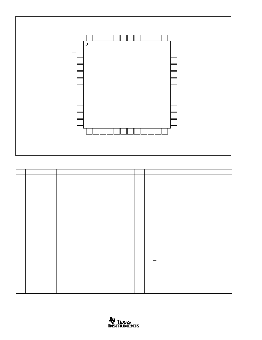
NC
No Internal Connection
26
NC
No Internal Connection
27
AGND
Analog Ground
28
AGND
Analog Ground
29
AGND
Analog Ground
30
V
REF
Internal Reference Voltage (1/2V Reference)
31
RSEL
Reference Mode Select (see Table I for
settings)
32
REFB
Bottom Reference Bypass
33
NC
No Internal Connection
34
REFT
Top Reference Bypass
35
NC
No Internal Connection
36
AV
DD
Analog Supply
37
AV
DD
Analog Supply
38
AGND
Analog Ground
39
AGND
Analog Ground
40
AGND
Analog Ground
41
I
IN
Analog Input
42
I
IN
Complementary Analog Input
43
DGND
Digital Ground
44
DGND
Digital Ground
45
DGND
Digital Ground
46
I
CLK
Convert Clock Input
47
I
DV
DD
Digital Supply
48
I
DV
DD
Digital Supply
PIN
I/O
NAME
DESCRIPTION
1
MSBI
Most Significant Bit Invert (HI = Binary Two's
Complement, LO = Straight Offset Binary)
2
OE
Tri-State (LO = Enabled, HI = Tri-State)
3
Mode Select
Duty Cycle Stablilizer (HI = Enabled,
LO = Normal Operation)
4
STPD
Standard Power Down (LO = Normal
Operation, HI = Enabled)
5
QPD
Quasi Power Down (LO = Normal Operation,
HI = Enabled)
6
GDRV
Output Driver Ground
7
GDRV
Output Driver Ground
8
VDRV
Output Driver Supply
9
VDRV
Output Driver Supply
10
O
D11 (MSB)
Data Bit 12
11
O
D10
Data Bit 11
12
O
D9
Data Bit 10
13
O
D8
Data Bit 9
14
O
D7
Data Bit 8
15
O
D6
Data Bit 7
16
O
D5
Data Bit 6
17
O
D4
Data Bit 5
18
O
D3
Data Bit 4
19
O
D2
Data Bit 3
20
O
D1
Data Bit 2
21
O
D0 (LSB)
Data Bit 1
22
NC
No Internal Connection
23
NC
No Internal Connection
24
OVR
Over-Range Indicator
PIN ASSIGNMENTS
PIN
I/O
NAME
DESCRIPTION
PIN CONFIGURATION
36
35
34
33
32
31
30
29
28
27
26
25
AV
DD
NC
REFT
NC
REFB
RSEL
V
REF
AGND
AGND
AGND
NC
NC
DV
DD
DV
DD
CLK
DGND
DGND
DGND
IN
IN
AGND
AGND
AGND
AV
DD
D8
D7
D6
D5
D4
D3
D2
D1
D0 (LSB)
NC
NC
OVR
1
2
3
4
5
6
7
8
9
10
11
12
MSBI
OE
Mode Select
STPD
QPD
GDRV
GDRV
VDRV
VDRV
D11 (MSB)
D10
D9
48
47
46
45
44
43
42
41
40
39
38
13
14
15
16
17
18
19
20
21
22
23
37
24
ADS5220

ADS5220
5
SBAS261A
www.ti.com
TIMING DIAGRAM
SYMBOL
DESCRIPTION
MIN
TYP
MAX
UNITS
t
CONV
Convert Clock Period
25
1
µ
s
ns
t
L
Clock Pulse LOW
8.75
12.5
ns
t
H
Clock Pulse HIGH
8.75
12.5
ns
t
D
Aperture Delay
3
ns
t
1
Data Hold Time, C
L
= 0pF
3.9
ns
t
2
New Data Delay Time, C
L
= 15pF max
12
ns
5 Clock Cycles
Data Invalid
t
D
t
L
t
H
t
CONV
N ≠ 5
N ≠ 4
N ≠ 3
N ≠ 2
N ≠ 1
N
N + 1
N + 2
Data Out
Clock
Analog In
N
t
2
N + 1
N + 2
N + 3
N + 4
N + 5
N + 6
N + 7
t
1