FEATURES
D
Maximum Sample Rate: 65MSPS
D
12-Bit Resolution
D
No Missing Codes
D
Power Dissipation: 996mW
D
CMOS Technology
D
Simultaneous Sample-and-Hold
D
70.5dB SNR at 10MHz IF
D
Internal and External References
D
3.3V Digital/Analog Supply
D
Serialized LVDS Outputs
D
Integrated Frame and Synch Patterns
D
MSB and LSB First Modes
D
Option to Double LVDS Clock Output Currents
D
Pin- and Format-Compatible Family
D
TQFP-80 PowerPAD
Package
APPLICATIONS
D
Portable Ultrasound Systems
D
Tape Drives
D
Test Equipment
D
Optical Networking
DESCRIPTION
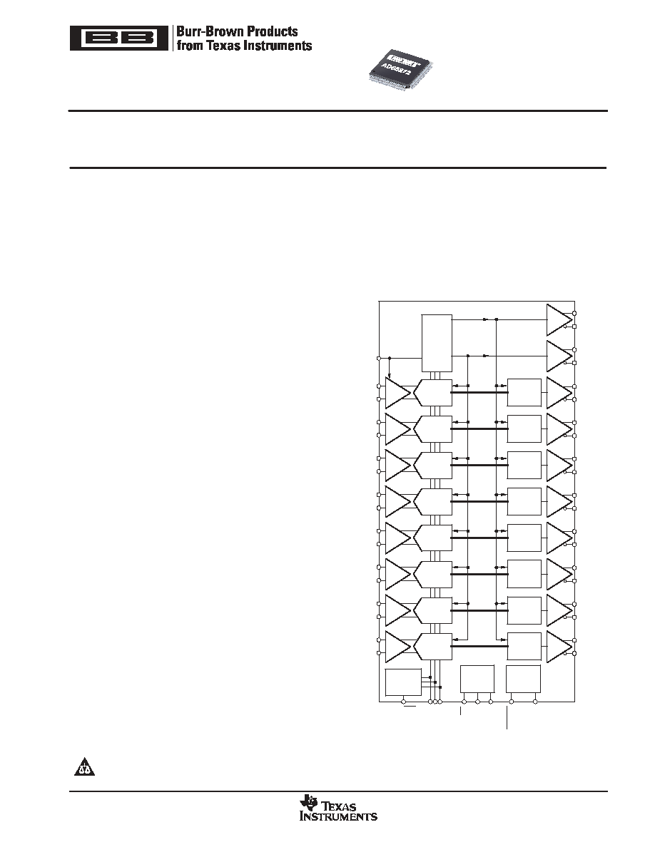
The ADS5272 is a high-performance, 65MSPS, 8-channel,
parallel analog-to-digital converter (ADC). Internal references
are provided, simplifying system design requirements. Low
power consumption allows for the highest of system
integration densities. Serial LVDS (low-voltage differential
signaling) outputs reduce the number of interface lines and
package size.
An integrated phase lock loop multiplies the incoming ADC
sampling clock by a factor of 12. This 12x clock is used in the
process of serializing the data output from each channel. The
12x clock is also used to generate a 1x and a 6x clock, both
of which are transmitted as LVDS clock outputs. The 6x clock
is denoted by the differential pair LCLKP and LCLKN, while the
1x clock is denoted by ADCLKP and ADCLKN. The word
output of each ADC channel can be transmitted either as MSB
or LSB first. The bit coinciding with the rising edge of the 1x
clock output is the first bit of the word. Data is to be latched by
the receiver on both the rising and falling edges of the 6x clock.
The ADS5272 provides internal references, or can optionally
be driven with external references. Best performance can be
achieved through the internal reference mode.
The device is available in a TQFP-80 PowerPAD package and
is specified over a -40
�
C to +85
�
C operating range.
12-Bit
ADC
PLL
S/H
Serializer
1X ADCLK
6X ADCLK
IN1
P
ADCLK
IN1
N
OUT1
P
OUT1
N
12-Bit
ADC
S/H
Serializer
IN2
P
IN2
N
OUT2
P
OUT2
N
12-Bit
ADC
S/H
Serializer
IN3
P
IN3
N
OUT3
P
OUT3
N
LCLK
P
LCLK
N
ADCLK
P
ADCLK
N
12-Bit
ADC
S/H
Serializer
IN4
P
IN4
N
OUT4
P
OUT4
N
12-Bit
ADC
S/H
Serializer
IN5
P
IN5
N
OUT5
P
OUT5
N
12-Bit
ADC
S/H
Serializer
IN6
P
IN6
N
OUT6
P
OUT6
N
12-Bit
ADC
S/H
Serializer
IN7
P
IN7
N
OUT7
P
OUT7
N
12-Bit
ADC
S/H
Serializer
Reference
IN8
P
IN8
N
RE
F
T
INT/EXT
V
CM
RE
F
B
OUT8
P
OUT8
N
Registers
SC
L
K
SD
AT
A
CS
Control
R
ESET
PD
PRODUCT PREVIEW
ADS5272
SBAS324 - JUNE 2004
8-Channel, 12-Bit, 65MSPS ADC
with Serial LVDS Interface
PRODUCT PREVIEW information concerns products in the formative or design
phase of development. Characteristic data and other specifications are design
goals. Texas Instruments reserves the right to change or discontinue these
products without notice.
www.ti.com
Copyright
2004, Texas Instruments Incorporated
Please be aware that an important notice concerning availability, standard warranty, and use in critical applications of Texas Instruments
semiconductor products and disclaimers thereto appears at the end of this data sheet.
PowerPAD is a registered trademark of Texas Instruments. All other trademarks are the property of their respective owners.

ADS5272
SBAS324 - JUNE 2004
www.ti.com
2
ABSOLUTE MAXIMUM RATINGS
(1)
Supply Voltage Range, AVDD
-0.3V to 3.8V
. . . . . . . . . . . . . . . . . .
Supply Voltage Range, LVDD
-0.3V to 3.8V
. . . . . . . . . . . . . . . . . .
Voltage Between AVSS and LVSS
-0.3V to 0.3V
. . . . . . . . . . . . . .
Voltage Between AVDD and LVDD
-0.3V to 0.3V
. . . . . . . . . . . . . .
Voltages Applied to External REF Pins
-0.3V to 2.4V
. . . . . . . . . .
All LVDS Data and Clock Outputs
-0.3V to 2.4V
. . . . . . . . . . . . . .
Analog Input Pins
-0.3V to 2.7V
. . . . . . . . . . . . . . . . . . . . . . . . . . . .
Peak Total Input Current (all inputs)
-30mA
. . . . . . . . . . . . . . . . . . .
Operating Free-Air Temperature Range, TA
-40
�
C to 85
�
C
. . . . . .
Lead Temperature 1.6mm (1/16
from case for 10s)
220
�
C
. . . . . .
(1) Stresses above these ratings may cause permanent damage.
Exposure to absolute maximum conditions for extended periods
may degrade device reliability. These are stress ratings only, and
functional operation of the device at these or any other conditions
beyond those specified is not supported.
This integrated circuit can be damaged by ESD. Texas
Instruments recommends that all integrated circuits be
handled with appropriate precautions. Failure to observe
proper handling and installation procedures can cause damage.
ESD damage can range from subtle performance degradation to
complete device failure. Precision integrated circuits may be more
susceptible to damage because very small parametric changes could
cause the device not to meet its published specifications.
ORDERING INFORMATION
(1)
PRODUCT
PACKAGE-LEAD
PACKAGE
DESIGNATOR
SPECIFIED
TEMPERATURE
RANGE
PACKAGE
MARKING
ORDERING
NUMBER
TRANSPORT
MEDIA, QUANTITY
ADS5272
HTQFP-80(2)
PFP
-40
�
C to +85
�
C
ADS5272IPFP
ADS5272IPFP
Tray, 96
ADS5272IPFPT
Tape and Reel, 250
(1) For the most current package and ordering information, see the Package Option Addendum located at the end of this data sheet.
(2) Thermal pad size: 4.69mm x 4.69mm (min), 6.20mm x 6.20mm (max).
RELATED PRODUCTS
MODEL
RESOLUTION (BITS)
SAMPLE RATE (MSPS)
CHANNELS
ADS5270
12
40
8
ADS5271
12
50
8
ADS5273
12
70
8
ADS5275
10
40
8
ADS5276
10
50
8
ADS5277
10
65
8
RECOMMENDED OPERATING CONDITIONS
ADS5272
MIN
TYP
MAX
UNIT
SUPPLIES AND REFERENCES
Analog Supply Voltage, AVDD
3.0
3.3
3.6
V
Output Driver Supply Voltage, LVDD
3.0
3.3
3.6
V
CLOCK INPUT AND OUTPUTS
ADCLK Input Sample Rate (low-voltage TTL)
20
65
MSPS
Low Level Voltage Clock Input
0.6
V
High Level Voltage Clock Input
VDD - 0.6
V
ADCLKP and ADCLKN Outputs (LVDS)
20
65
MHz
LCLKP and LCLKN Outputs (LVDS)(1)
120
390
MHz
Operating Free-Air Temperature, TA
-40
+85
�
C
Thermal Characteristics
q
JA
21
�
C/W
q
JC
68
�
C/W
(1) 6
�
ADCLK.
REFERENCE SELECTION
MODE
INT/EXT
DESCRIPTION
2.0VPP Internal Reference
1
Default with internal pull-up.
External Reference
0
Internal reference is powered down. Common mode of external reference should be within
50mV of VCM. VCM is derived from the internal bandgap voltage.
PRODUCT PREVIEW

ADS5272
SBAS324 - JUNE 2004
www.ti.com
3
ELECTRICAL CHARACTERISTICS
TMIN = -40
�
C, and TMAX = +85
�
C. Typical values are at TA = 25
�
C, clock frequency = maximum specified, 50% clock duty cycle, AVDD = 3.3V,
LVDD = 3.3V, -1dBFS, internal voltage reference, and LVDS buffer current at 3.5mA per channel, unless otherwise noted.
ADS5272
PARAMETER
TEST CONDITIONS
MIN
TYP
MAX
UNITS
DC ACCURACY
No Missing Codes
Assured
DNL
Differential Nonlinearity
f
IN
= 5MHz
-0.9
�
0.5
0.9
LSB
INL
Integral Nonlinearity
f
IN
= 5MHz
-2.0
�
0.6
2.0
LSB
Offset Error
(1)
TBD
�
0.2
TBD
%FS
Offset Temperature Coefficient
14
ppm/
�
C
Fixed Attenuation in Channel
(2)
1
%FS
Variable Attenuation in Channel
(3)
�
0.2
%FS
Gain Error
(4)
REF
T
- REF
B
TBD
�
1.0
TBD
%FS
Gain Temperature Coefficient
(5)
44
ppm/
�
C
POWER SUPPLY
I
CC
Total Supply Current
V
IN
= FS, F
IN
= 5MHz
302
mA
I(AVDD)
Analog Supply Current
V
IN
= FS, F
IN
= 5MHz
TBD
mA
I(LVDD)
Digital Output Driver Supply Current
V
IN
= FS, F
IN
= 5MHz, LVDS Into 100
Load
TBD
mA
Power Dissipation
996
TBD
mW
Power Down
Clock Running
90
mW
REFERENCE VOLTAGES
VREF
T
Reference Top (internal)
1.95
2.0
2.05
V
VREF
B
Reference Bottom (internal)
0.95
1.0
1.05
V
V
CM
Common-Mode Voltage
1.45
1.5
1.55
V
V
CM
Output Current
(6)
�
50mV Change in Voltage
�
2
mA
VREF
T
Reference Top (external)
1.875
V
VREF
B
Reference Bottom (external)
1.125
V
External Reference Input Current
(7)
2.0
mA
ANALOG INPUT
Differential Input Capacitance
7.0
pF
Analog Input Common-Mode Range
V
CM
�
0.05
V
Differential Input Voltage Range
1.5
2.02
V
PP
Voltage Overload Recovery Time
Differential Input Signal at 4V
PP
Recovery to Within 1% of Code
4.0
CLK Cycles
Input Bandwidth
-3dBFS
300
MHz
DIGITAL DATA OUTPUTS
Data Bit Rate
340
780
MBPS
SERIAL INTERFACE
SCLK
Serial Clock Input Frequency
20
MHz
V
IN
LOW
Input Low Voltage
0
0.6
V
V
IN
HIGH
Input High Voltage
2.1
VDD
V
Input Current
�
10
�
A
Input Pin Capacitance
5.0
pF
(1)
Offset error is the deviation of the average code from mid-code for a zero input. Offset error is expressed in terms of % of full-scale.
(2)
Fixed attenuation in the channel arises due to a fixed attenuation of about 1% in the sample-and-hold amplifier. When the differential voltage at the analog input pins are
changed from -V
REF
to +V
REF
, the swing of the output code is expected to deviate from the full-scale code (4096LSB) by the extent of this fixed attenuation [V
REF
is defined
as (REF
T
- REF
B
)].
(3)
Variable attenuation in the channel refers to the attenuation of the signal in the channel over and above the fixed attenuation.
(4)
The reference voltages are trimmed at production so that (VREF
T
- VREF
B
) is within
�
25mV of the ideal value of 1V. It does not include fixed attenuation.
(5)
The gain temperature coefficient refers to the temperature coefficient of the attenuation in the channel. It does not account for the variation of the reference voltages with
temperature.
(6)
V
CM
provides the common-mode current for the inputs of all eight channels when the inputs are AC-coupled. The V
CM
output current specified is the additional drive of
the V
CM
buffer if loaded externally.
(7)
Average current drawn from the reference pins in the external reference mode.
PRODUCT PREVIEW

ADS5272
SBAS324 - JUNE 2004
www.ti.com
4
AC CHARACTERISTICS
TMIN = -40
�
C, TMAX = +85
�
C. Typical values are at TA = 25
�
C, clock frequency = maximum specified, 50% clock duty cycle, AVDD = 3.3V, LVDD = 3.3V,
-1dBFS, internal voltage reference, and LVDS buffer current at 3.5mA per channel, unless otherwise noted.
ADS5272
PARAMETER
CONDITIONS
MIN
TYP
MAX
UNITS
DYNAMIC CHARACTERISTICS
fIN = 1MHz
87
dBc
SFDR
Spurious-Free Dynamic Range
fIN = 5MHz
TBD
85
dBc
SFDR
Spurious-Free Dynamic Range
fIN = 10MHz
85
dBc
fIN = 20MHz
83
dBc
fIN = 1MHz
90
dBc
HD2 2nd-Order Harmonic Distortion
fIN = 5MHz
TBD
90
dBc
HD2 2nd-Order Harmonic Distortion
fIN = 10MHz
89
dBc
fIN = 20MHz
86
dBc
fIN = 1MHz
87
dBc
HD3 3rd-Order Harmonic Distortion
fIN = 5MHz
TBD
85
dBc
HD3 3rd-Order Harmonic Distortion
fIN = 10MHz
85
dBc
fIN = 20MHz
83
dBc
fIN = 1MHz
70.5
dBFS
SNR
Signal-to-Noise Ratio
fIN = 5MHz
TBD
70.5
dBFS
SNR
Signal-to-Noise Ratio
fIN = 10MHz
70.5
dBFS
fIN = 20MHz
70.5
dBFS
fIN = 1MHz
70
dBFS
SINAD
Signal-to-Noise and Distortion
fIN = 5MHz
TBD
70
dBFS
SINAD
Signal-to-Noise and Distortion
fIN = 10MHz
70
dBFS
fIN = 20MHz
70
dBFS
IMD
Two-Tone Intermodulation Distortion
f1 = 9.5MHz at -7dBFS
-85
dBFS
IMD
Two-Tone Intermodulation Distortion
f2 = 10.2MHz at -7dBFS
-85
dBFS
ENOB
Effective Number of Bits
fIN = 5MHz
11.3
Bits
Crosstalk
Signal Applied to 7 Channels;
Measurement Taken on the Channel with
No Input Signal
-90
dBc
LVDS DIGITAL DATA AND CLOCK OUTPUTS
Test conditions at IO = 3.5mA, RLOAD = 100
, and CLOAD = 9pF. IO refers to the current setting for the LVDS buffer. RLOAD is the differential load resistance
between the differential LVDS pair. CLOAD is the effective single-ended load capacitance between the differential LVDS pins and ground. CLOAD includes the
receiver input parasitics as well as the routing parasitics. Measurements are done with a transmission line of 100
differential impedance between the device and
the load. All LVDS specifications are functionally tested, but not parametrically tested.
PARAMETER
CONDITIONS
MIN
TYP
MAX
UNITS
DC SPECIFICATIONS(1)
VOH Output Voltage High, OUTP or OUTN
RLOAD = 100
�
1%; See LVDS Timing Diagram, Page 7
1375
1500
mV
VOL Output Voltage Low, OUTP or OUTN
RLOAD = 100
�
1%
900
1025
mV
VOD
Output Differential Voltage,
OUTP - OUTN
RLOAD = 100
�
1%
300
350
400
mV
VOS Output Offset Voltage(2)
RLOAD = 100
�
1%; See LVDS Timing Diagram, Page 7
1100
1200
1300
mV
CO
Output Capacitance(3)
VCM = 1.5V
4
pF
VOD
Change in
VOD
Between 0 and 1
RLOAD = 100
�
1%
25
mV
VOS Change Between 0 and 1
RLOAD = 100
�
1%
25
mV
ISOUT
Output Short-Circuit Current
Drivers Shorted to Ground
40
mA
ISOUTNP Output Current
Drivers Shorted Together
12
mA
DRIVER AC SPECIFICATIONS
Clock
Clock Signal Duty Cycle
6
�
ADCLK
45
50
55
%
Minimum Data Setup TIme(4, 5)
650
ps
Minimum Data Hold Time(4, 5)
650
ps
tRISE/tFALL VOD Rise Time or VOD Fall Time
IO = 2.5mA
400
IO = 3.5mA
250
ps
IO = 4.5mA
200
ps
IO = 6mA
150
ps
(1) The DC specifications refer to the condition where the LVDS outputs are not switching, but are permanently at a valid logic level 0 or 1.
(2) VOS refers to the common-mode of OUTP and OUTN.
(3) Output capacitance inside the device, from either OUTP or OUTN to ground.
(4) Refer to the LVDS application note (SBAA118) for a description of data setup and hold times.
(5) Setup and hold time specifications take into account the effect of jitter on the output data and clock. These specifications also assume that the data and clock
paths are perfectly matched within the receiver. Any mismatch in these paths within the receiver would appear as reduced timing margins.
PRODUCT PREVIEW

ADS5272
SBAS324 - JUNE 2004
www.ti.com
5
SWITCHING CHARACTERISTICS
TMIN = -40
�
C, TMAX = +85
�
C. Typical values are at TA = 25
�
C, clock frequency = maximum specified, 50% clock duty cycle, AVDD = 3.3V,
LVDD = 3.3V, -1dBFS, internal voltage reference, and LVDS buffer current at 3.5mA per channel, unless otherwise noted.
ADS5272
PARAMETER
CONDITIONS
MIN
TYP
MAX
UNITS
SWITCHING SPECIFICATIONS
t
SAMPLE
25
50
ns
t
D
(A)
Aperture Delay
2.5
ns
Aperture Jitter (uncertainty)
1
ps
t
D
(pipeline)
Latency
6.5
cycles
t
PROP
Propagation Delay
5
ns
SERIAL INTERFACE TIMING
Data is shifted in MSB first.
PARAMETER
DESCRIPTION
MIN
TYP
MAX
UNIT
t1
Serial CLK Period
50
ns
t2
Serial CLK High Time
25
ns
t3
Serial CLK Low Time
25
ns
t4
Minimum Data Setup Time
5
ns
t5
Minimum Data Hold Time
5
ns
PRODUCT PREVIEW
Start Sequence
t
1
MSB
D6
D5
D4
D3
D2
D1
D0
t
2
t
3
t
4
t
5
ADCLK
CS
SCLK
SDATA
Outputs change on
next rising clock edge
after CS goes high.
Data latched on
each rising edge of SCLK.