 | –≠–ª–µ–∫—Ç—Ä–æ–Ω–Ω—ã–π –∫–æ–º–ø–æ–Ω–µ–Ω—Ç: ADS574KE | –°–∫–∞—á–∞—Ç—å:  PDF PDF  ZIP ZIP |
© 1991 Burr-Brown Corporation
PDS-1104F
Printed in U.S.A. July, 1993
ADS574
FEATURES
q
REPLACES ADC574 FOR NEW DESIGNS
q
COMPLETE SAMPLING A/D WITH
REFERENCE, CLOCK AND
MICROPROCESSOR INTERFACE
q
FAST ACQUISITION AND CONVERSION:
25
µ
s max
q
ELIMINATES EXTERNAL SAMPLE/HOLD
IN MOST APPLICATIONS
q
GUARANTEED AC AND DC PERFORMANCE
q
SINGLE +5V SUPPLY OPERATION
q
LOW POWER: 100mW max
q
PACKAGE OPTIONS: 0.6" and 0.3" DIPs,
SOIC
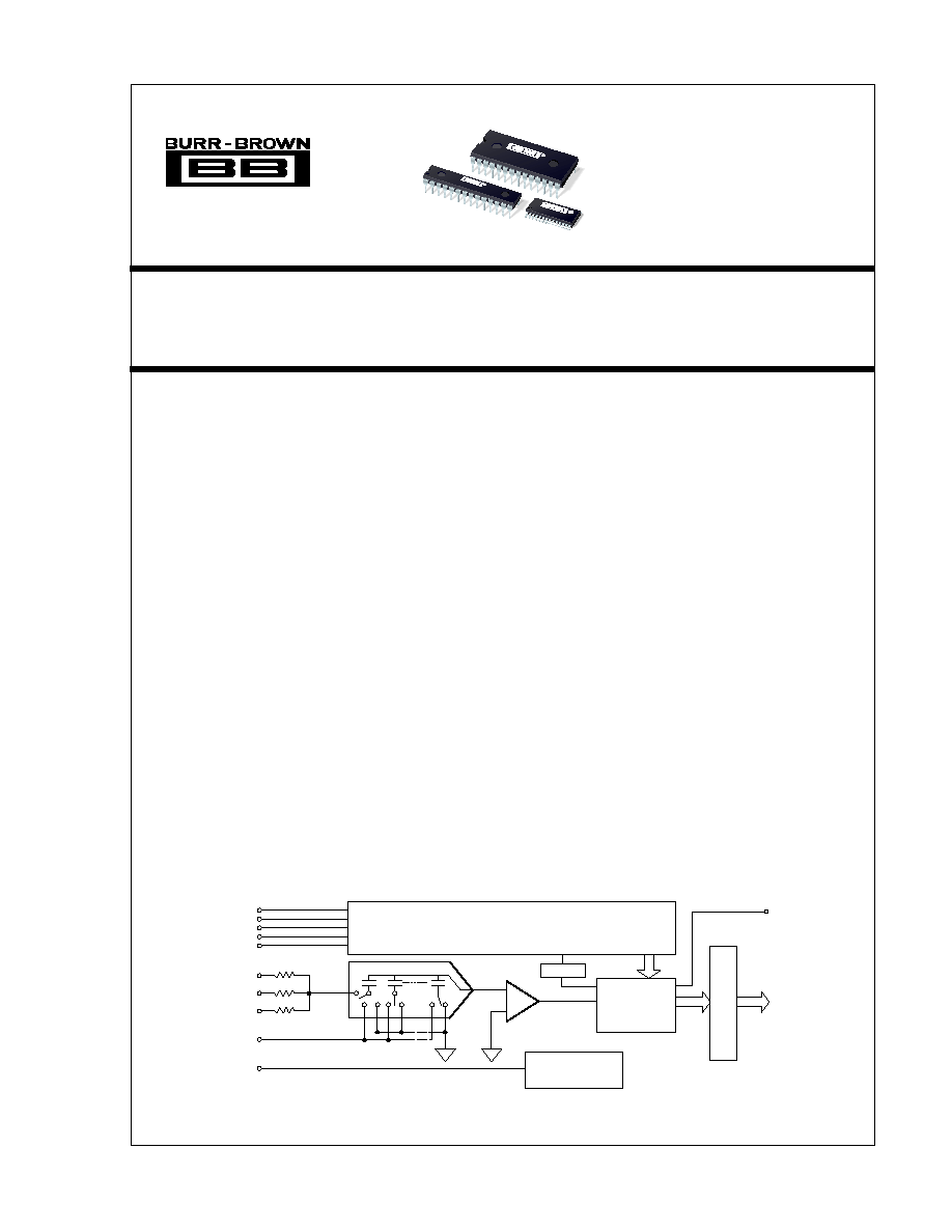
DESCRIPTION
The ADS574 is a 12-bit successive approximation
analog-to-digital converter using an innovative
capacitor array (CDAC) implemented in low-power
CMOS technology. This is a drop-in replacement for
ADC574 models in most applications, with internal
sampling, much lower power consumption, and capa-
bility to operate from a single +5V supply.
The ADS574 is complete with internal clock, micro-
processor interface, three-state outputs, and internal
scaling resistors for input ranges of 0V to +10V, 0V to
+20V,
±
5V, or
±
10V. The maximum throughput time
for 12-bit conversions is 25
µ
s over the full operating
temperature range, including both acquisition and con-
version.
Complete user control over the internal sampling func-
tion facilitates elimination of external sample/hold
amplifiers in most existing designs.
The ADS574 requires +5V, with ≠12V or ≠15V op-
tional, depending on usage. No +15V supply is re-
quired. Available packages include 0.3" or 0.6" wide
28-pin plastic DIPs and 28-lead SOICs.
Microprocessor-Compatible Sampling
CMOS ANALOG-TO-DIGITAL CONVERTER
Comparator
2.5V Reference
Input
CDAC
10V Range
20V Range
Bipolar Offset
≠
+
2.5V Reference
Output
Control
Inputs
2.5V
Reference
Clock
Successive
Approximation
Register
Control Logic
Three-State Buffers
Status
Parallel
Data
Output
Æ
International Airport Industrial Park ∑ Mailing Address: PO Box 11400, Tucson, AZ 85734 ∑ Street Address: 6730 S. Tucson Blvd., Tucson, AZ 85706 ∑ Tel: (520) 746-1111 ∑ Twx: 910-952-1111
Internet: http://www.burr-brown.com/ ∑ FAXLine: (800) 548-6133 (US/Canada Only) ∑ Cable: BBRCORP ∑ Telex: 066-6491 ∑ FAX: (520) 889-1510 ∑ Immediate Product Info: (800) 548-6132
ADS574
ADS574
ADS574
Æ
ADS574
2
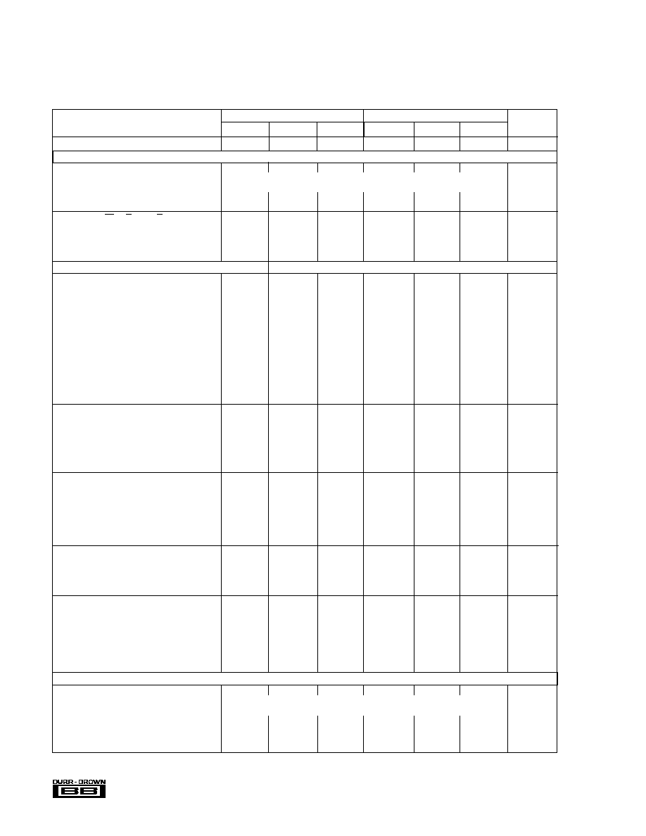
ADS574JE, JP, JU
ADS574KE, KP, KU
PARAMETER
MIN
TYP
MAX
MIN
TYP
MAX
UNITS
RESOLUTION
12
T
Bits
INPUTS
ANALOG
Voltage Ranges: Unipolar
0 to +10, 0 to +20
V
Bipolar
±
5,
±
10
V
Impedance:
0 to +10V,
±
5V
15
21
T
T
k
±
10V, 0V to +20V
60
84
T
T
k
DIGITAL (CE, CS, R/C, A
O
, 12/8)
Voltages: Logic 1
+2.0
+5.5
T
T
V
Logic 0
≠0.5
+0.8
T
T
V
Current
≠5
0.1
+5
T
T
T
µ
A
Capacitance
5
T
pF
TRANSFER CHARACTERISTICS
DC ACCURACY
At +25
∞
C
Linearity Error
±
1
±
1/2
LSB
Unipolar Offset Error (adjustable to zero)
±
2
T
LSB
Bipolar Offset Error (adjustable to zero)
±
10
±
4
LSB
Full-Scale Calibration Error
(1)
(adjustable to zero)
±
0.25
T
% of FS
(2)
No Missing Codes Resolution (Diff. Linearity)
12
12
Bits
T
MIN
to T
MAX
(3)
Linearity Error
±
1
±
1/2
LSB
Full-Scale Calibration Error
±
0.47
±
0.37
% of FS
Unipolar Offset
±
4
±
3
LSB
Bipolar Offset
±
12
±
5
LSB
No Missing Codes Resolution
12
12
Bits
AC ACCURACY
(4)
Spurious Free Dynamic Range
73
78
76
T
dB
Total Harmonic Distortion
≠77
≠72
T
≠75
dB
Signal-to-Noise Ratio
69
72
71
T
dB
Signal-to-(Noise + Distortion) Ratio
68
71
70
T
dB
Intermodulation Distortion
≠75
T
(F
IN1
= 10kHz, F
IN2
= 11.5kHz)
TEMPERATURE COEFFICIENTS
(5)
Unipolar Offset
±
1
T
ppm/
∞
C
Bipolar Offset
±
2
T
ppm/
∞
C
Full-Scale Calibration
±
12
T
ppm/
∞
C
POWER SUPPLY SENSITIVITY
Change in Full-Scale Calibration
(6)
+4.75V < V
DD
< +5.25V
±
1/2
T
LSB
CONVERSION TIME (Including Acquisition Time)
t
AQ
+ t
C
at 25
∞
C:
8-Bit Cycle
16
18
T
T
µ
s
12-Bit Cycle
22
25
T
T
µ
s
12-Bit Cycle, T
MIN
to T
MAX
22
25
T
T
µ
s
SAMPLING DYNAMICS
Sampling Rate
40
T
kHz
Aperture Delay, t
AP
With V
EE
= +5V
20
T
ns
With V
EE
= 0V to ≠15V
4.0
T
µ
s
Aperture Uncertainty (Jitter)
With V
EE
= +5V
300
T
ps, rms
With V
EE
= 0V to ≠15V
30
T
ns, rms
OUTPUTS
DIGITAL (DB
11
- DB
0
, STATUS)
Output Codes: Unipolar
Unipolar Straight Binary (USB)
Bipolar
Bipolar Offset Binary (BOB)
Logic Levels: Logic 0 (I
SINK
= 1.6mA)
+0.4
T
V
Logic 1 (I
SOURCE
= 500
µ
A)
+2.4
T
V
Leakage, Data Bits Only, High-Z State
≠5
0.1
+5
T
T
T
µ
A
Capacitance
5
T
pF
SPECIFICATIONS
ELECTRICAL
At T
A
= T
MIN
to T
MAX
, V
DD
= +5V, V
EE
= ≠15V to +5V, sampling frequency of 40kHz, and f
IN
= 10kHz, unless otherwise specified.

3
Æ
ADS574
INTERNAL REFERENCE VOLTAGE
Voltage
+2.4
+2.5
+2.6
T
T
T
V
Source Current Available for External Loads
0.5
T
mA
POWER SUPPLY REQUIREMENTS
Voltage: V
EE
(7)
≠16.5
V
DD
T
T
V
V
DD
+4.5
+5.5
T
T
V
Current: I
EE
(7)
(V
EE
= ≠15V)
≠1
T
mA
I
DD
+13
+20
T
T
mA
Power Dissipation (T
MIN
to T
MAX
)
(V
EE
= 0V to +5V)
65
100
T
T
mW
TEMPERATURE RANGE
Specification
0
+70
T
T
∞
C
Operating:
≠40
+85
T
T
∞
C
Storage
≠65
+150
T
T
∞
C
T
Same specification as ADS574JE, JP, JU.
NOTES: (1) With fixed 50
resistor from REF OUT to REF IN. This parameter is also adjustable to zero at +25
∞
C. (2) FS in this specification table means Full Scale
Range. That is, for a
±
10V input range, FS means 20V; for a 0 to +10V range, FS means 10V. (3) Maximum error at T
MIN
and T
MAX
. (4) Based on using V
EE
=
+5V, which starts a conversion immediately upon a convert command. Using V
EE
= 0V to ≠15V makes the ADS574/ADS774 emulate standard ADC574 operation.
In this mode, the internal sample/hold acquires the input signal after receiving the convert command, and does not assume that the input level has been stable
before the convert command arrives. (5) Using internal reference. (6) This is worst case change in accuracy from accuracy with a +5V supply. (7) V
EE
is optional,
and is only used to set the mode for the internal sample/hold. When V
EE
= ≠15V, I
EE
= ≠1mA typ; when V
EE
= 0V, I
EE
=
±
5
µ
A typ; when V
EE
= +5V, I
EE
= +167
µ
A
typ.
SPECIFICATIONS
(CONT)
ELECTRICAL
At T
A
= T
MIN
to T
MAX
, V
DD
= +5V, V
EE
= ≠15V to +5V, sampling frequency of 40kHz, and f
IN
= 10kHz, unless otherwise specified.
ADS574JE, JP, JU
ADS574KE, KP, KU
PARAMETER
MIN
TYP
MAX
MIN
TYP
MAX
UNITS
The information provided herein is believed to be reliable; however, BURR-BROWN assumes no responsibility for inaccuracies or omissions. BURR-BROWN assumes
no responsibility for the use of this information, and all use of such information shall be entirely at the user's own risk. Prices and specifications are subject to change
without notice. No patent rights or licenses to any of the circuits described herein are implied or granted to any third party. BURR-BROWN does not authorize or warrant
any BURR-BROWN product for use in life support devices and/or systems.
ABSOLUTE MAXIMUM RATINGS
V
EE
to Digital Common ....................................................... +V
DD
to ≠16.5V
V
DD
to Digital Common .............................................................. 0V to +7V
Analog Common to Digital Common ....................................................
±
1V
Control Inputs (CE, CS, A
O
, 12/8, R/C)
to Digital Common .................................................. ≠0.5V to V
DD
+0.5V
Analog Inputs (Ref In, Bipolar Offset, 10V
IN
)
to Analog Common ......................................................................
±
16.5V
20V
IN
to Analog Common ..................................................................
±
24V
Ref Out .......................................................... Indefinite Short to Common,
Momentary Short to V
DD
Max Junction Temperature ............................................................ +165
∞
C
Power Dissipation ........................................................................ 1000mW
Lead Temperature (soldering,10s) ................................................. +300
∞
C
Thermal Resistance,
JA
: Plastic DIPs ........................................ 100
∞
C/W
SOIC ................................................... 100
∞
C/W
ELECTROSTATIC
DISCHARGE SENSITIVITY
This integrated circuit can be damaged by ESD. Burr-Brown
recommends that all integrated circuits be handled with
appropriate precautions. Failure to observe proper handling
and installation procedures can cause damage.
ESD damage can range from subtle performance degrada-
tion to complete device failure. Precision integrated circuits
may be more susceptible to damage because very small
parametric changes could cause the device not to meet its
published specifications.
PACKAGE/ORDERING INFORMATION
PACKAGE DRAWING
TEMPERATURE
LINEARITY
PRODUCT
PACKAGE
NUMBER
(1)
SINAD
(2)
RANGE
ERROR (LSB)
ADS574JE
0.3" Plastic DIP
246
68
0
∞
C to +70
∞
C
±
1
ADS574KE
0.3" Plastic DIP
246
70
0
∞
C to +70
∞
C
±
1/2
ADS574JP
0.6" Plastic DIP
215
68
0
∞
C to +70
∞
C
±
1
ADS574KP
0.6" Plastic DIP
215
70
0
∞
C to +70
∞
C
±
1/2
ADS574JU
SOIC
217
68
0
∞
C to +70
∞
C
±
1
ADS574KU
SOIC
217
70
0
∞
C to +70
∞
C
±
1/2
NOTES: (1) For detailed drawing and dimension table, please see end of data sheet, or Appendix C of Burr-Brown IC Data Book. (2) SINAD is Signal-to-(Noise
and Distortion) expressed in dB.

Æ
ADS574
4
CONNECTION DIAGRAM
1
2
3
4
5
Power-Up Reset
Control
Logic
Clock
12 Bits
Succesive Approximation Register
12
Bits
Three-State Buffers and Control
Nibble A
Nibble B
Nibble C
≠
+
CDAC
6
7
8
9
10
11
12
13
14
28
27
26
25
24
23
22
21
20
19
18
17
16
15
+5VDC Supply
(V )
DD
A
O
≠
R/C
≠
12/8
CE
NC*
2.5V Ref
Out
Analog
Common
2.5V Ref
In
Bipolar
Offset
10V Range
20V Range
Digital
Common
DB0 (LSB)
DB1
DB2
DB3
DB4
DB5
DB6
DB7
DB8
DB9
DB10
DB11 (MSB)
Status
*Not Internally Connected
2.5V
Reference
CS
V
EE
(Mode Control)

5
Æ
ADS574
TYPICAL PERFORMANCE CURVES
At T
A
= +25
∞
C, V
DD
= V
EE
= +5V; Bipolar
±
10V Input Range; sampling frequency of 40kHz; unless otherwise specified. All plots use 4096 point FFTs.
SIGNAL/(NOISE + DISTORTION) vs
INPUT FREQUENCY AND AMBIENT TEMPERATURE
Signal/(Noise + Distortion) (dB)
Input Frequency (kHz)
75
70
65
0.1
1
10
100
≠55∞C
+25∞C
+125∞C
FREQUENCY SPECTRUM (±10V, 2kHz Input)
Magnitude (dB)
Frequency (kHz)
0
≠60
≠120
0
5
10
20
≠100
≠80
≠40
≠20
15
S/(N + D) = 73.1dB
THD = ≠94.5dB
SNR = 73.1dB
FREQUENCY SPECTRUM (±10V, 19kHz Input)
Magnitude (dB)
Frequency (kHz)
0
≠60
≠120
0
5
10
20
≠100
≠80
≠40
≠20
15
S/(N + D) = 68.4dB
THD = ≠75.9dB
SNR = 69.3dB
FREQUENCY SPECTRUM (±1V, 19kHz Input)
Magnitude (dB)
Frequency (kHz)
0
≠60
≠120
0
5
10
20
≠100
≠80
≠40
≠20
15
S/(N + D) = 53.3dB
THD = ≠74.5dB
SNR = 53.3dB
SPURIOUS FREE DYNAMIC RANGE, SNR AND THD
vs INPUT FREQUENCY
Spurious Free Dynamic Range, SNR, THD (dB)
Input Frequency (kHz)
100
80
60
0.1
1
10
100
90
70
POWER SUPPLY REJECTION
vs SUPPLY RIPPLE FREQUENCY
Power Supply Rejection Ratio (V/V in dB)
Supply Ripple Frequency (Hz)
80
40
10
10
100
1k
10M
60
20
10k
100k
1M