 | –≠–ª–µ–∫—Ç—Ä–æ–Ω–Ω—ã–π –∫–æ–º–ø–æ–Ω–µ–Ω—Ç: ADS7803BP | –°–∫–∞—á–∞—Ç—å:  PDF PDF  ZIP ZIP |

ADS7803
Autocalibrating, 4-Channel, 12-Bit
ANALOG-TO-DIGITAL CONVERTER
DESCRIPTION
The ADS7803 is a monolithic CMOS 12-bit analog-
to-digital converter with internal sample/hold and four-
channel multiplexer. It is designed and tested for full
dynamic performance with input signals to 50kHz. An
autocalibration cycle guarantees a total unadjusted
error within
±
3/4LSB over the specified temperature
range, eliminating the need for offset or gain adjust-
ment. The 5V single-supply requirements and stan-
dard CS, RD, and WR control signals make the part
easy to use in microprocessor applications. Conver-
sion results are available in two bytes through an 8-bit
three-state output bus.
The ADS7803 is available in a 28-pin plastic DIP and
28-lead PLCC, fully specified for operation over the
industrial ≠40
∞
C to +85
∞
C temperature range.
Three-State
Input/Output
CS
Control
Logic
RD
WR
SFR
BUSY
8-Bit
Data Bus
Capacitor Array
Sampling ADC
Analog
Multiplexer
AIN0
AIN1
AIN2
AIN3
Calibration
Microcontroller
and Memory
A0
A1
Clock
V
REF
+
V
REF
≠
Address
Latch and
Decoder
International Airport Industrial Park ∑ Mailing Address: PO Box 11400 ∑ Tucson, AZ 85734 ∑ Street Address: 6730 S. Tucson Blvd. ∑ Tucson, AZ 85706
Tel: (520) 746-1111 ∑ Twx: 910-952-1111 ∑ Cable: BBRCORP ∑ Telex: 066-6491 ∑ FAX: (520) 889-1510 ∑ Immediate Product Info: (800) 548-6132
Æ
FEATURES
q
LOW POWER: 10mW plus Power Down
q
SIGNAL-TO-(NOISE + DISTORTION)
RATIO OVER TEMPERATURE:
69dB min with f
IN
= 1kHz
66dB min with f
IN
= 50kHz
q
FAST CONVERSION TIME: 8.5
µ
s
Including Acquisition (117kHz Sampling
Rate)
q
DC PERFORMANCE OVER
TEMPERATURE:
±
3/4 LSB max Total Error
±
1/4 LSB max Channel Mismatch
q
FOUR-CHANNEL INPUT MULTIPLEXER
q
SINGLE SUPPLY: +5V
q
PIN COMPATIBLE WITH ADC7802
©
1991 Burr-Brown Corporation
PDS-1126A
Printed in U.S.A. August, 1993
Æ
ADS7803
2
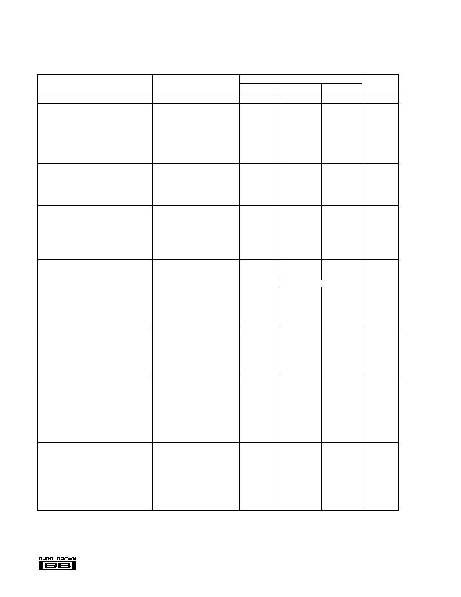
SPECIFICATIONS
ELECTRICAL
V
A
= V
D
= V
REF
+ = 5V
±
5%; V
REF
≠ = AGND = DGND = 0V; CLK = 2MHz external, T
A
= ≠40
∞
C to +85
∞
C, after calibration at any temperature, unless otherwise specified.
NOTES: (1) For (V
REF
+) ≠ (V
REF
≠) as low as 4.5V, the total error will typically not exceed
±
1LSB. (2) After calibration cycle, without external adjustment. Includes gain
(full scale) error, offset error, integral nonlinearity, differential nonlinearity, and drift.
The information provided herein is believed to be reliable; however, BURR-BROWN assumes no responsibility for inaccuracies or omissions. BURR-BROWN
assumes no responsibility for the use of this information, and all use of such information shall be entirely at the user's own risk. Prices and specifications are subject
to change without notice. No patent rights or licenses to any of the circuits described herein are implied or granted to any third party. BURR-BROWN does not
authorize or warrant any BURR-BROWN product for use in life support devices and/or systems.
ADS7803BP/ADS7803BN
PARAMETER
CONDITIONS
MIN
TYP
MAX
UNITS
RESOLUTION
12
Bits
ANALOG INPUT
Voltage Input Range
V
REF
+ = 5V, V
REF
≠ = 0V
0
5
V
Input Capacitance
50
pF
On State Bias Current
100
nA
Off State Bias Current
T
A
= +25
∞
C
10
nA
T
A
= ≠40
∞
C to +85
∞
C
100
nA
On Resistance Multiplexer
2
k
Off Resistance Multiplexer
10
M
Channel Separation
500Hz
92
dB
REFERENCE INPUT
For Specified Performance: V
REF
+
V
REF
+
V
A
5
V
V
REF
≠
0
V
For Derated Performance
(1)
: V
REF
+
4.5
V
A
V
V
REF
≠
0
1
V
Input Reference Current
V
REF
+ = 5V, V
REF
≠ = 0V
10
100
µ
A
THROUGHPUT TIMING
Conversion Time With External Clock (Including
CLK = 2MHz
8.5
µ
s
Multiplexer Settling Time and Acquisition Time)
CLK = 1MHz
17
µ
s
CLK = 500kHz
34
µ
s
With Internal Clock Using Recommended
T
A
= +25
∞
C
10
µ
s
Clock Components
T
A
= ≠40
∞
C to +85
∞
C
10
µ
s
Multiplexer Settling Time to 0.01%
460
ns
Multiplexer Access Time
20
ns
DC ACCURACY
Total Error, All Channels
(2)
±
1/2
±
3/4
LSB
Differential Nonlinearity
±
1/4
±
1/2
LSB
No Missing Codes
Guaranteed
Gain Error
All Channels
±
1/8
±
1/4
LSB
Gain Error Drift
Between Calibration Cycles
±
0.2
ppm/
∞
C
Offset Error
All Channels
±
1/8
±
1/4
LSB
Offset Error Drift
Between Calibration Cycles
±
0.2
ppm/
∞
C
Channel-to-Channel Mismatch
±
1/4
LSB
Power Supply Sensitivity
V
A
= V
D
= 4.75V to 5.25V
±
1/8
LSB
AC ACCURACY
Signal-to-(Noise + Distortion) Ratio
f
IN
= 1kHz
69
71
dB
f
IN
= 50kHz
66
69
dB
Total Harmonic Distortion
f
IN
= 50kHz
≠75
dB
Signal-to-Noise Ratio
f
IN
= 50kHz
70
dB
Spurious Free Dynamic Range
f
IN
= 1kHz
90
dB
f
IN
= 50kHz
82
dB
SAMPLING DYNAMICS
Full Power Bandwidth
≠3dB
4
MHz
Aperture Delay
SFR D2 LOW
2500
ns
Offset Error
SRF D2 HIGH
5
ns
SFR D2 LOW
±
1/8
±
1/4
LSB
SFR D2 HIGH, Internal Clock or
±
1/2
±
1
LSB
Sampling Command Synchronous
to External Clock
SFR D2 HIGH, Sampling Command
±
4
LSB
Asynchronous to External Clock
DIGITAL INPUTS
All Pins Other Than CLK: V
IL
0.8
V
V
IH
2.4
V
Input Current
T
A
= +25
∞
C, V
IN
= 0 to V
D
1
µ
A
T
A
= ≠40
∞
C to +85
∞
C, V
IN
= 0 to V
D
10
µ
A
CLK Input: V
IL
0.8
V
V
IH
3.5
V
I
IL
10
µ
A
I
IH
1.5
mA
I
IH
Power Down Mode (D3 in SFR HIGH)
100
nA

3
Æ
ADS7803
ORDERING INFORMATION
MINIMUM SIGNAL-TO-
SPECIFICATION
(NOISE + DISTORTION)
MAXIMUM TOTAL
TEMPERATURE
MODEL
RATIO, dB
ERROR, LSB
RANGE
1-24
25-99
100+
ADS7803BN
69
±
3/4
≠40
∞
C to +85
∞
C
ADS7803BP
69
±
3/4
≠40
∞
C to +85
∞
C
SPECIFICATIONS
(CONT)
ELECTRICAL
V
A
= V
D
= V
REF
+ = 5V
±
5%; V
REF
≠ = AGND = DGND = 0V; CLK = 2MHz external, T
A
= ≠40
∞
C to +85
∞
C, after calibration at any temperature, unless otherwise specified.
ADS7803BP/ADS7803BN
PARAMETER
CONDITIONS
MIN
TYP
MAX
UNITS
DIGITAL OUTPUTS
V
OL
I
SINK
= 1.6mA
0.4
V
V
OH
I
SOURCE
= 200
µ
A
4
V
Leakage Current
High-Z State, V
OUT
= 0V to V
D
±
1
µ
A
Output Capacitance
High-Z State
4
15
pF
POWER SUPPLIES
Supply Voltage for Specified Performance: V
A
4.75
5
5.25
V
V
D
V
A
V
D
4.75
5
5.25
V
Supply Current: I
A
1
2.5
mA
I
D
Logic Input Pins HIGH or LOW
1
2
mA
Power Dissipation
WR = RD = CS = BUSY = HIGH
10
mW
Power Down Mode
See Table III
50
µ
W
TEMPERATURE RANGE
Specification
≠40
+85
∞
C
Storage
≠65
+150
∞
C
PIN CONFIGURATIONS
Top View
DIP
Top View
LCC
SFR
AIN0
AIN1
AIN2
AIN3
V
REF
+
V
REF
≠
DGND
V
D
D7
D6
D5
D4
D3
1
2
3
4
5
6
7
8
9
10
11
12
13
14
28
27
26
25
24
23
22
21
20
19
18
17
16
15
V
A
AGND
CAL (SHC)
A1
A0
CLK
BUSY
HBE
WR
CS
RD
D0
D1
D2
AIN3
V
REF
+
V
REF
≠
DGND
V
D
D7
D6
5
6
7
8
9
10
11
25
24
23
22
21
20
19
A1
A0
CLK
BUSY
HBE
WR
CS
AIN2
AIN1
AIN0
SFR
V
A
AGND
CAL (SHC)
D5
D4
D3
D2
D1
D0
RD
4
3
2
1
28
27
26
12
13
14
15
16
17
18
PACKAGE INFORMATION
PACKAGE DRAWING
MODEL
PACKAGE
NUMBER
(1)
ADC7803BN
28-Pin LCC
251
ADS7803BP
28-Pin Plastic DIP
215
NOTE: (1) For detailed drawing and dimension table, please see end of data
sheet, or Appendix D of Burr-Brown IC Data Book.
V
A
to Analog Ground .......................................................................... 6.5V
V
D
to Digital Ground ........................................................................... 6.5V
Pin V
A
to Pin V
D
...............................................................................
±
0.3V
Analog Ground to Digital Ground ........................................................
±
1V
Control Inputs to Digital Ground ................................ ≠0.3V to V
D
+ 0.3V
Analog Input Voltage to Analog Ground .................... ≠0.3V to V
D
+ 0.3V
Maximum Junction Temperature ..................................................... 150
∞
C
Internal Power Dissipation ............................................................. 875mW
Lead Temperature (soldering, 10s) ............................................... +300
∞
C
Thermal Resistance,
JA
: Plastic DIP .......................................... 75
∞
C/W
PLCC .................................................. 75
∞
C/W
ABSOLUTE MAXIMUM RATINGS
Æ
ADS7803
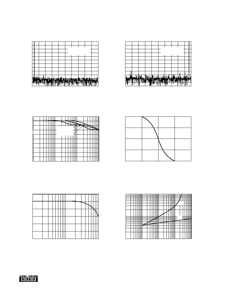
4
FREQUENCY SPECTRUM (1kHz f
IN
)
Frequency (kHz)
0
0
≠20
≠40
≠60
≠80
≠100
Magnitude (dB)
≠120
10
20
30
40
50
S/(N + D) = 71.4dB
f
SAMPLING
= 100kHz
TYPICAL PERFORMANCE CURVES
At V
A
= V
D
= V
REF
+ = 5V, V
REF
≠ = AGND = 0V, T
A
= +25
∞
C, dynamic performance based on 2048 point FFTs, unless otherwise noted.
FREQUENCY SPECTRUM (48kHz f
IN
)
Frequency (kHz)
0
0
≠20
≠40
≠60
≠80
≠100
Magnitude (dB)
≠120
10
20
30
40
50
S/(N + D) = 69.2dB
f
SAMPLING
= 100kHz
CHANNEL SEPARATION vs FREQUENCY
1
Frequency of 5Vp-p Signal on Channel AIN2 (kHz)
10
100
1k
100
80
60
40
20
Channel Separation (dB)
0
Channel AIN3
Channel AIN1
Channel AIN0
SIGNAL/(NOISE + DISTORTION)
vs INPUT FREQUENCY
Input Frequency (kHz)
Signal/(Noise + Distortion) (dB)
66
0.5
50
5
72
70
68
1
2
3
10
20
3
POWER SUPPLY REJECTION vs FREQUENCY
0.1
Frequency (kHz)
1
100
1000
10
10
1
Full-Scale Error vs
Change in Supply Voltage (mV/V)
0.1
V
D
V
A
CODE TRANSITION NOISE
Analog Input Voltage ≠ Expected Code Center (LSBs)
0
100
75
50
25
Conversion Yielding Expected Code (%)
0
1
0.25
0.5
0.75

5
Æ
ADS7803
TYPICAL PERFORMANCE CURVES
(CONT)
At V
A
= V
D
= V
REF
+ = 5V, V
REF
≠ = AGND = 0V, T
A
= +25
∞
C, dynamic performance based on 2048 point FFTs , unless otherwise noted.
THEORY OF OPERATION
ADS7803 uses the advantages of advanced CMOS technol-
ogy (logic density, stable capacitors, precision analog
switches, and low power consumption) to provide a precise
12-bit analog-to-digital converter with on-chip sampling and
four-channel analog-input multiplexer.
The input stage consists of an analog multiplexer with an
address latch to select from four input channels.
The converter stage consists of an advanced successive
approximation architecture using charge redistribution on a
capacitor network to digitize the input signal. A tempera-
ture-stabilized differential auto-zeroing circuit is used to
minimize offset errors in the comparator.
Linearity errors in the binary weighted main capacitor
network are corrected using a capacitor trim network and
correction factors stored in on-chip memory. The correction
terms are calculated by an on-chip microcontroller during a
calibration cycle, initiated either by power-up or by applying
an external calibration signal at any time. During conver-
sion, the correct trim capacitors are switched into the main
capacitor array as needed to correct the conversion accuracy.
With all of the capacitors in both the main array and the trim
array on the same chip, excellent stability is achieved, both
over temperature and over time.
For flexibility, timing circuits include both an internal clock
generator and an input for an external clock to synchronize
with external systems. Standard control signals and three-
state input/output registers simplify interfacing ADS7803 to
most micro-controllers, microprocessors or digital storage
systems.
The on-chip sampling provides excellent dynamic perfor-
mance for input signals to 50kHz, and has a full-power ≠3dB
bandwidth of 4MHz. Full control over sample-to-hold
timing is available for applications where this is critical.
Finally, this performance is matched with the low-power
advantages of CMOS structures to allow a typical power
consumption of 10mW, with a 50
µ
W power down option.
OPERATION
BASIC OPERATION
Figure 1 shows the simple circuit required to operate
ADS7803 in the Transparent Mode, converting a single
input channel. A convert command on pin 20 (WR) starts a
conversion. Pin 22 (BUSY) will output a LOW during the
conversion process (including sample acquisition and con-
version), and rises only after the conversion is completed.
The two bytes of output data can then be read using pin 18
(RD) and pin 21 (HBE).
FIGURE 1. Basic Operation.
SFR
AIN0
AIN1
AIN2
AIN3
V
REF
+
V
REF
≠
DGND
V
D
D7
D6
D5
D4
D3
V
A
AGND
CAL
A1
A0
CLK
BUSY
HBE
WR
CS
RD
D0
D1
D2
1
2
3
4
5
6
7
8
9
10
11
12
13
14
28
27
26
25
24
23
22
21
20
19
18
17
16
15
Read Command
Convert
Command
High Byte
Enable
Command
BUSY
10nF
+5V
10µF
100k
NC
10µF
10nF
+
+5V
NC
Data Bit 7
Data Bit 6
Data Bit 5
Data Bit 4
Data Bit 3
BUSY
LOW
LOW
LOW
Data Bit 11
(MSB)
HBE Input
LOW
HBE Input
HIGH
Data Bit 8
Data Bit 9
Data Bit 10
Data Bit 0
(LSB)
Data Bit 1
Data Bit 2
HBE Input
HIGH
HBE Input
LOW
0 ≠5V
Input
+
INTERNAL CLOCK FREQUENCY vs TEMPERATURE
Ambient Temperature (∞C)
≠50
100
≠25
75
0
25
50
R
CLOCK
= 70k
Clock Frequency (MHz)
0.9
1.15
1.1
1.05
1
0.95
10
1
INTERNAL CLOCK FREQUENCY vs R
CLOCK
R
CLOCK
(k
)
Clock Frequency (MHz)
0.1
10
1k
100