 | –≠–ª–µ–∫—Ç—Ä–æ–Ω–Ω—ã–π –∫–æ–º–ø–æ–Ω–µ–Ω—Ç: ADS7804P | –°–∫–∞—á–∞—Ç—å:  PDF PDF  ZIP ZIP |

©
1992 Burr-Brown Corporation
PDS-1156C
Printed in U.S.A. February, 1996
FEATURES
q
100kHz min SAMPLING RATE
q
STANDARD
±
10V INPUT RANGE
q
72dB min SINAD WITH 45kHz INPUT
q
±
0.45 LSB max INL
q
DNL: 12 Bits "No Missing Codes"
q
SINGLE +5V SUPPLY OPERATION
q
PIN-COMPATIBLE WITH 16-BIT ADS7805
q
USES INTERNAL OR EXTERNAL
REFERENCE
q
COMPLETE WITH S/H, REF, CLOCK, ETC.
q
FULL PARALLEL DATA OUTPUT
q
100mW max POWER DISSIPATION
q
28-PIN 0.3" PLASTIC DIP AND SOIC
ADS7804
DESCRIPTION
The ADS7804 is a complete 12-bit sampling A/D
using state-of-the-art CMOS structures. It contains a
complete 12-bit, capacitor-based, SAR A/D with S/H,
reference, clock, interface for microprocessor use, and
three-state output drivers.
The ADS7804 is specified at a 100kHz sampling rate,
and guaranteed over the full temperature range. Laser-
trimmed scaling resistors provide an industry-
standard
±
10V input range, while the innovative de-
sign allows operation from a single +5V supply, with
power dissipation under 100mW.
The 28-pin ADS7804 is available in a plastic 0.3" DIP
and in an SOIC, both fully specified for operation over
the industrial ≠40
∞
C to +85
∞
C range.
12-Bit 10
µ
s Sampling CMOS
ANALOG-to-DIGITAL CONVERTER
Successive Approximation Register and Control Logic
Clock
Output
Latches
and
Three
State
Drivers
Three
State
Parallel
Data
Bus
BUSY
Comparator
BYTE
CS
R/C
CDAC
Internal
+2.5V Ref
Buffer
4k
±10V Input
REF
CAP
20k
4k
10k
Æ
DEMO BOARD
AVAILABLE
International Airport Industrial Park ∑ Mailing Address: PO Box 11400, Tucson, AZ 85734 ∑ Street Address: 6730 S. Tucson Blvd., Tucson, AZ 85706 ∑ Tel: (520) 746-1111 ∑ Twx: 910-952-1111
Internet: http://www.burr-brown.com/ ∑ FAXLine: (800) 548-6133 (US/Canada Only) ∑ Cable: BBRCORP ∑ Telex: 066-6491 ∑ FAX: (520) 889-1510 ∑ Immediate Product Info: (800) 548-6132
ADS7804
ADS7804

2
Æ
ADS7804
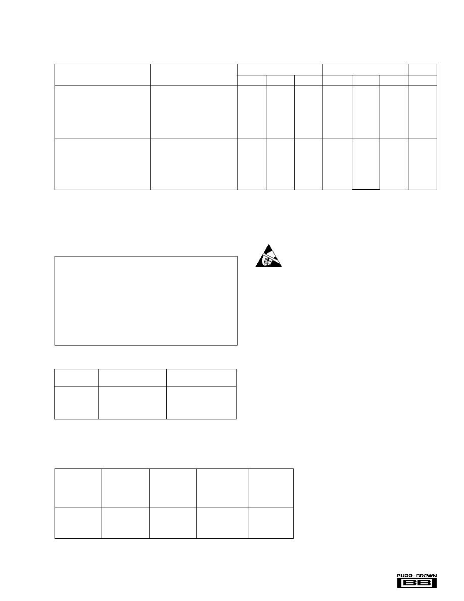
RESOLUTION
12
*
Bits
ANALOG INPUT
Voltage Ranges
±
10V
*
V
Impedance
23
*
k
Capacitance
35
*
pF
THROUGHPUT SPEED
Conversion Time
5.7
8
*
*
µ
s
Complete Cycle
Acquire and Convert
10
*
µ
s
Throughput Rate
100
*
kHz
DC ACCURACY
Integral Linearity Error
±
0.9
±
0.45
LSB
(1)
Differential Linearity Error
±
0.9
±
0.45
LSB
No Missing Codes
*
Bits
Transition Noise
(2)
0.1
*
LSB
Full Scale Error
(3,4)
±
0.5
±
0.25
%
Full Scale Error Drift
±
7
±
5
ppm/
∞
C
Full Scale Error
(3,4)
Ext. 2.5000V Ref
±
0.5
±
0.25
%
Full Scale Error Drift
Ext. 2.5000V Ref
±
2
*
ppm/
∞
C
Bipolar Zero Error
(3)
±
10
±
10
mV
Bipolar Zero Error Drift
±
2
*
ppm/
∞
C
Power Supply Sensitivity
+4.75V < V
D
< +5.25V
±
0.5
*
LSB
(V
DIG
= V
ANA
= V
D
)
AC ACCURACY
Spurious-Free Dynamic Range
f
IN
= 45kHz
80
*
dB
(5)
Total Harmonic Distortion
f
IN
= 45kHz
≠80
*
dB
Signal-to-(Noise+Distortion)
f
IN
= 45kHz
70
72
dB
Signal-to-Noise
f
IN
= 45kHz
70
72
dB
Full-Power Bandwidth
(6)
250
*
kHz
SAMPLING DYNAMICS
Aperture Delay
40
*
ns
Aperture Jitter
*
Transient Response
FS Step
2
*
µ
s
Overvoltage Recovery
(7)
150
*
ns
REFERENCE
Internal Reference Voltage
2.48
2.5
2.52
*
*
*
V
Internal Reference Source Current
1
*
µ
A
(Must use external buffer.)
Internal Reference Drift
8
ppm/
∞
C
External Reference Voltage Range
2.3
2.5
2.7
*
*
*
V
for Specified Linearity
External Reference Current Drain
Ext. 2.5000V Ref
100
*
µ
A
DIGITAL INPUTS
Logic Levels
V
IL
≠0.3
+0.8
*
*
V
V
IH
+2.0
V
D
+0.3V
*
*
V
I
IL
±
10
*
µ
A
I
IH
±
10
*
µ
A
DIGITAL OUTPUTS
Data Format
Data Coding
V
OL
I
SINK
= 1.6mA
+0.4
*
V
V
OH
I
SOURCE
= 500
µ
A
+4
*
V
Leakage Current
High-Z State,
±
5
*
µ
A
V
OUT
= 0V to V
DIG
Output Capacitance
High-Z State
15
15
pF
DIGITAL TIMING
Bus Access Time
83
*
ns
Bus Relinquish Time
83
*
ns
SPECIFICATIONS
ELECTRICAL
At T
A
= ≠40
∞
C to +85
∞
C, f
S
= 100kHz, and V
DIG
= V
ANA
= +5V, using internal reference, unless otherwise specified.
ADS7804P, U
ADS7804PB, UB
PARAMETER
CONDITIONS
MIN
TYP
MAX
MIN
TYP
MAX
UNITS
The information provided herein is believed to be reliable; however, BURR-BROWN assumes no responsibility for inaccuracies or omissions. BURR-BROWN
assumes no responsibility for the use of this information, and all use of such information shall be entirely at the user's own risk. Prices and specifications are subject
to change without notice. No patent rights or licenses to any of the circuits described herein are implied or granted to any third party. BURR-BROWN does not
authorize or warrant any BURR-BROWN product for use in life support devices and/or systems.
Guaranteed
Sufficient to meet AC specs
Parallel 12 bits
Binary Two's Complement
Æ
ADS7804
3
ELECTROSTATIC
DISCHARGE SENSITIVITY
Electrostatic discharge can cause damage ranging from
performance degradation to complete device failure. Burr-
Brown Corporation recommends that all integrated circuits be
handled and stored using appropriate ESD protection
methods.
SPECIFICATIONS
(CONT)
ELECTRICAL
At T
A
= ≠40
∞
C to +85
∞
C, f
S
= 100kHz, and V
DIG
= V
ANA
= +5V, using internal reference, unless otherwise specified.
ADS7804P, U
ADS7804PB, UB
PARAMETER
CONDITIONS
MIN
TYP
MAX
MIN
TYP
MAX
UNITS
ABSOLUTE MAXIMUM RATINGS
Analog Inputs: V
IN
.............................................................................
±
25V
CAP ................................... +V
ANA
+0.3V to AGND2 ≠0.3V
REF .......................................... Indefinite Short to AGND2
Momentary Short to V
ANA
Ground Voltage Differences: DGND, AGND1, AGND2 .................
±
0.3V
V
ANA
....................................................................................................... 7V
V
DIG
to V
ANA
..................................................................................... +0.3V
V
DIG
....................................................................................................... 7V
Digital Inputs ........................................................... ≠0.3V to +V
DIG
+0.3V
Maximum Junction Temperature ................................................... +165
∞
C
Internal Power Dissipation ............................................................. 825mW
Lead Temperature (soldering, 10s) ............................................... +300
∞
C
PACKAGE INFORMATION
PACKAGE DRAWING
PRODUCT
PACKAGE
NUMBER
(1)
ADS7804P
Plastic DIP
246
ADS7804PB
Plastic DIP
246
ADS7804U
SOIC
217
ADS7804UB
SOIC
217
NOTE: (1) For detailed drawing and dimension table, please see end of data
sheet, or Appendix C of Burr-Brown IC Data Book.
MINIMUM
SIGNAL-TO-
MAXIMUM
(NOISE +
SPECIFICATION
LINEARITY
DISTORTION)
TEMPERATURE
PRODUCT
ERROR (LSB)
RATIO (dB)
RANGE
PACKAGE
ADS7804P
±
0.9
70
≠40
∞
C to +85
∞
C
Plastic DIP
ADS7804PB
±
0.45
72
≠40
∞
C to +85
∞
C
Plastic DIP
ADS7804U
±
0.9
70
≠40
∞
C to +85
∞
C
SOIC
ADS7804UB
±
0.45
72
≠40
∞
C to +85
∞
C
SOIC
ORDERING INFORMATION
POWER SUPPLIES
Specified Performance
V
DIG
Must be
V
ANA
+4.75
+5
+5.25
*
*
*
V
V
ANA
+4.75
+5
+5.25
*
*
*
V
+I
DIG
0.3
*
mA
+I
ANA
16
*
mA
Power Dissipation
f
S
= 100kHz
100
*
mW
TEMPERATURE RANGE
Specified Performance
≠40
+85
*
*
∞
C
Derated Performance
≠55
+125
*
*
∞
C
Storage
≠65
+150
∑
∑
∞
C
Thermal Resistance (
JA
)
Plastic DIP
75
*
∞
C/W
SOIC
75
*
∞
C/W
NOTES: (1) LSB means Least Significant Bit. For the 12-bit,
±
10V input ADS7804, one LSB is 4.88mV. (2) Typical rms noise at worst case transitions and
temperatures. (3) As measured with fixed resistors shown in Figure 4. Adjustable to zero with external potentiometer. (4) Full scale error is the worst case of ≠Full
Scale or +Full Scale untrimmed deviation from ideal first and last code transitions, divided by the transition voltage (not divided by the full-scale range) and includes
the effect of offset error. (5) All specifications in dB are referred to a full-scale
±
10V input. (6) Full-Power Bandwidth defined as Full-Scale input frequency at which
Signal-to-(Noise + Distortion) degrades to 60dB, or 10 bits of accuracy. (7) Recovers to specified performance after 2 x FS input overvoltage.

4
Æ
ADS7804
1
V
IN
Analog Input. See Figure 7.
2
AGND1
Analog Ground. Used internally as ground reference point.
3
REF
Reference Input/Output. 2.2
µ
F tantalum capacitor to ground.
4
CAP
Reference Buffer Capacitor. 2.2
µ
F tantalum capacitor to ground.
5
AGND2
Analog Ground.
6
D15 (MSB)
O
Data Bit 11. Most Significant Bit (MSB) of conversion results. Hi-Z state when CS is HIGH, or when R/C is LOW.
7
D14
O
Data Bit 10. Hi-Z state when CS is HIGH, or when R/C is LOW.
8
D13
O
Data Bit 9. Hi-Z state when CS is HIGH, or when R/C is LOW.
9
D12
O
Data Bit 8. Hi-Z state when CS is HIGH, or when R/C is LOW.
10
D11
O
Data Bit 7. Hi-Z state when CS is HIGH, or when R/C is LOW.
11
D10
O
Data Bit 6. Hi-Z state when CS is HIGH, or when R/C is LOW.
12
D9
O
Data Bit 5. Hi-Z state when CS is HIGH, or when R/C is LOW.
13
D8
O
Data Bit 4. Hi-Z state when CS is HIGH, or when R/C is LOW.
14
DGND
Digital Ground.
15
D7
O
Data Bit 3. Hi-Z state when CS is HIGH, or when R/C is LOW.
16
D6
O
Data Bit 2. Hi-Z state when CS is HIGH, or when R/C is LOW.
17
D5
O
Data Bit 1. Hi-Z state when CS is HIGH, or when R/C is LOW.
18
D4
O
Data Bit 0. Lease Significant Bit (LSB) of conversion results. Hi-Z state when CS is HIGH, or when R/C is LOW.
19
D3
O
LOW when CS LOW, R/C HIGH. Hi-Z state when CS is HIGH, or when R/C is LOW.
20
D2
O
LOW when CS LOW, R/C HIGH. Hi-Z state when CS is HIGH, or when R/C is LOW.
21
D1
O
LOW when CS LOW, R/C HIGH. Hi-Z state when CS is HIGH, or when R/C is LOW.
22
D0 (LSB)
O
LOW when CS LOW, R/C HIGH. Hi-Z state when CS is HIGH, or when R/C is LOW.
23
BYTE
I
Selects 8 most significant bits (LOW) or 8 least significant bits (HIGH).
24
R/C
I
With CS LOW and BUSY HIGH, a Falling Edge on R/C Initiates a New Conversion. With CS LOW, a rising edge on R/C
enables the parallel output.
25
CS
I
Internally OR'd with R/C. If R/C LOW, a falling edge on CS initiates a new conversion.
26
BUSY
O
At the start of a conversion, BUSY goes LOW and stays LOW until the conversion is completed and the digital outputs
have been updated.
27
V
ANA
Analog Supply Input. Nominally +5V. Decouple to ground with 0.1
µ
F ceramic and 10
µ
F tantalum capacitors.
28
V
DIG
Digital Supply Input. Nominally +5V. Connect directly to pin 27. Must be
V
ANA
.
DIGITAL
PIN #
NAME
I/O
DESCRIPTION
TABLE I. Pin Assignments.
CHARACTERIZATION CURVES
Call factory for updated data sheet which includes character-
ization curves.
PIN CONFIGURATION
V
DIG
V
ANA
BUSY
CS
R/C
BYTE
DZ
DZ
DZ
DZ
D0 (LSB)
D1
D2
D3
V
IN
AGND1
REF
CAP
AGND2
D11 (MSB)
D10
D9
D8
D7
D6
D5
D4
DGND
1
2
3
4
5
6
7
8
9
10
11
12
13
14
28
27
26
25
24
23
22
21
20
19
18
17
16
15
ADS7804

Æ
ADS7804
5
BASIC OPERATION
Figure 1 shows a basic circuit to operate the ADS7804 with
a full parallel data output. Taking R/C (pin 24) LOW for a
minimum of 40ns (6
µ
s max) will initiate a conversion.
BUSY (pin 26) will go LOW and stay LOW until the
conversion is completed and the output registers are up-
dated. Data will be output in Binary Two's Complement
with the MSB on pin 6. BUSY going HIGH can be used to
latch the data. All convert commands will be ignored while
BUSY is LOW.
The ADS7804 will begin tracking the input signal at the end
of the conversion. Allowing 10
µ
s between convert com-
mands assures accurate acquisition of a new signal.
The offset and gain are adjusted internally to allow external
trimming with a single supply. The external resistors com-
pensate for this adjustment and can be left out if the offset
and gain will be corrected in software (refer to the Calibra-
tion section).
STARTING A CONVERSION
The combination of CS (pin 25) and R/C (pin 24) LOW for
a minimum of 40ns immediately puts the sample/hold of the
ADS7804 in the hold state and starts conversion `n'. BUSY
(pin 26) will go LOW and stay LOW until conversion `n' is
completed and the internal output register has been updated.
All new convert commands during BUSY LOW will be
ignored. CS and/or R/C must go HIGH before BUSY goes
HIGH or a new conversion will be initiated without suffi-
cient time to acquire a new signal.
The ADS7804 will begin tracking the input signal at the end
of the conversion. Allowing 10
µ
s between convert com-
mands assures accurate acquisition of a new signal. Refer to
Table II for a summary of CS, R/C, and BUSY states and
Figures 3 through 5 for timing diagrams.
CS and R/C are internally OR'd and level triggered. There
is not a requirement which input goes LOW first when
initiating a conversion. If, however, it is critical that CS or
R/C initiates conversion `n', be sure the less critical input is
LOW at least 10ns prior to the initiating input.
To reduce the number of control pins, CS can be tied LOW
using R/C to control the read and convert modes. This will
have no effect when using the internal data clock in the serial
output mode. However, the parallel output will become
active whenever R/C goes HIGH. Refer to the Reading
Data section.
FIGURE 1. Basic Operation.
CS
R/C
BUSY
OPERATION
1
X
X
None. Databus is in Hi-Z state.
0
1
Initiates conversion "n". Databus remains
in Hi-Z state.
0
1
Initiates conversion "n". Databus enters Hi-Z
state.
0
1
Conversion "n" completed. Valid data from
conversion "n" on the databus.
1
1
Enables databus with valid data from
conversion "n".
1
0
Enables databus with valid data from
conversion "n-1"
(1)
. Conversion n in process.
0
0
Enables databus with valid data from
conversion "n-1"
(1)
. Conversion "n" in process.
0
0
New conversion initiated without acquisition
of a new signal. Data will be invalid. CS and/or
R/C must be HIGH when BUSY goes HIGH.
X
X
0
New convert commands ignored. Conversion
"n" in process.
NOTE: (1) See Figures 2 and 3 for constraints on data valid from
conversion "n-1".
Table II. Control Line Functions for "Read" and "Convert".
1
2
3
4
5
6
7
8
9
10
11
12
13
14
28
27
26
25
24
23
22
21
20
19
18
17
16
15
ADS7804
200
33.2k
+5V
0.1µF
10µF
+
+
2.2µF
+
+
2.2µF
Convert Pulse
40ns min
6µs max
B4
B5
B6
B7
B2
B1
B0 (LSB)
B3
B10
B9
B8
B11
B12
B13
B14
B15 (MSB)