 | –≠–ª–µ–∫—Ç—Ä–æ–Ω–Ω—ã–π –∫–æ–º–ø–æ–Ω–µ–Ω—Ç: ADS7806 | –°–∫–∞—á–∞—Ç—å:  PDF PDF  ZIP ZIP |

Low-Power 12-Bit Sampling CMOS
ANALOG-to-DIGITAL CONVERTER
DESCRIPTION
The ADS7806 is a low-power 12-bit sampling analog-
to-digital using state-of-the-art CMOS structures. It
contains a complete 12-bit, capacitor-based, SAR A/D
with S/H, clock, reference, and microprocessor inter-
face with parallel and serial output drivers.
The ADS7806 can acquire and convert to full 12-bit
accuracy in 25
µ
s max while consuming only 35mW
max. Laser-trimmed scaling resistors provide standard
industrial input ranges of
±
10V and 0V to +5V. In
addition, a 0V to +4V range allows development of
complete single supply systems.
The 28-pin ADS7806 is available in a plastic 0.3" DIP
and in an SOIC, both fully specified for operation over
the industrial ≠40
∞
C to +85
∞
C temperature range.
CDAC
6k
40k
10k
BUSY
Parallel
and
Serial
Data
Out
Comparator
Buffer
20k
R1
IN
R2
IN
REF
Successive Approximation Register and Control Logic
Clock
Power
Down
BYTE
CS
R/C
40k
Internal
+2.5V Ref
Reference
Power
Down
Serial Data
Clock
Parallel Data
CAP
Serial Data
8
FEATURES
q
35mW max POWER DISSIPATION
q
50
µ
W POWER DOWN MODE
q
25
µ
s max ACQUISITION AND
CONVERSION
q
±
1/2LSB max INL AND DNL
q
72dB min SINAD WITH 1kHz INPUT
q
±
10V, 0V TO +5V, AND 0V TO +4V INPUT
RANGES
q
SINGLE +5V SUPPLY OPERATION
q
PARALLEL AND SERIAL DATA OUTPUT
q
PIN-COMPATIBLE WITH 16-BIT ADS7807
q
USES INTERNAL OR EXTERNAL
REFERENCE
q
28-PIN 0.3" PLASTIC DIP AND SOIC
ADS7806
International Airport Industrial Park ∑ Mailing Address: PO Box 11400 ∑ Tucson, AZ 85734 ∑ Street Address: 6730 S. Tucson Blvd. ∑ Tucson, AZ 85706
Tel: (520) 746-1111 ∑ Twx: 910-952-1111 ∑ Cable: BBRCORP ∑ Telex: 066-6491 ∑ FAX: (520) 889-1510 ∑ Immediate Product Info: (800) 548-6132
Æ
©
1992 Burr-Brown Corporation
PDS-1158C
Printed in U.S.A. November, 1994

2
Æ
ADS7806
SPECIFICATIONS
ELECTRICAL
At T
A
= ≠40
∞
C to +85
∞
C, f
S
= 40kHz, V
DIG
= V
ANA
= +5V, using internal reference and fixed resistors shown in Figure 7b, unless otherwise specified.
ADS7806P, U
ADS7806PB, UB
PARAMETER
CONDITIONS
MIN
TYP
MAX
MIN
TYP
MAX
UNITS
Parallel 12-bits in 2-bytes; Serial
Binary Two's Complement or Straight Binary
The information provided herein is believed to be reliable; however, BURR-BROWN assumes no responsibility for inaccuracies or omissions. BURR-BROWN
assumes no responsibility for the use of this information, and all use of such information shall be entirely at the user's own risk. Prices and specifications are subject
to change without notice. No patent rights or licenses to any of the circuits described herein are implied or granted to any third party. BURR-BROWN does not
authorize or warrant any BURR-BROWN product for use in life support devices and/or systems.
RESOLUTION
12
*
Bits
ANALOG INPUT
Voltage Ranges
±
10, 0 to +5, 0 to +4
V
Impedance
(See Table II)
Capacitance
35
*
pF
THROUGHPUT SPEED
Conversion Time
20
*
µ
s
Complete Cycle
Acquire and Convert
25
*
µ
s
Throughput Rate
40
*
kHz
DC ACCURACY
Integral Linearity Error
±
0.15
±
0.9
*
±
0.45
LSB
(1)
Differential Linearity Error
±
0.15
±
0.9
*
±
0.45
LSB
No Missing Codes
Guaranteed
*
Bits
Transition Noise
(2)
0.1
*
LSB
Gain Error
±
0.2
±
0.1
%
Full Scale Error
(3,4)
±
0.5
±
0.25
%
Full Scale Error Drift
±
7
±
5
ppm/
∞
C
Full Scale Error
(3,4)
Ext. 2.5000V Ref
±
0.5
±
0.25
%
Full Scale Error Drift
Ext. 2.5000V Ref
±
0.5
*
ppm/
∞
C
Bipolar Zero Error
(3)
±
10V Range
±
10
*
mV
Bipolar Zero Error Drift
±
10V Range
±
0.5
*
ppm/
∞
C
Unipolar Zero Error
(3)
0V to 5V, 0V to 4V Ranges
±
3
*
mV
Unipolar Zero Error Drift
0V to 5V, 0V to 4V Ranges
±
0.5
*
ppm/
∞
C
Recovery Time to Rated Accuracy
2.2
µ
F Capacitor to CAP
1
*
ms
from Power Down
(5)
Power Supply Sensitivity
+4.75V < V
S
< +5.25V
±
0.5
*
LSB
(V
DIG
= V
ANA
= V
S
)
AC ACCURACY
Spurious-Free Dynamic Range
f
IN
= 1kHz,
±
10V
80
90
*
*
dB
(6)
Total Harmonic Distortion
f
IN
= 1kHz,
±
10V
≠90
≠80
*
*
dB
Signal-to-(Noise+Distortion)
f
IN
= 1kHz,
±
10V
70
73
72
*
dB
Signal-to-Noise
f
IN
= 1kHz,
±
10V
70
73
72
*
dB
Usable Bandwidth
(7)
130
*
kHz
Full Power Bandwidth (-3dB)
600
*
kHz
SAMPLING DYNAMICS
Aperture Delay
40
*
ns
Aperture Jitter
20
*
ps
Transient Response
FS Step
5
*
µ
s
Overvoltage Recovery
(8)
750
*
ns
REFERENCE
Internal Reference Voltage
No Load
2.48
2.5
2.52
*
*
*
V
Internal Reference Source Current
1
*
µ
A
(Must use external buffer.)
Internal Reference Drift
8
*
ppm/
∞
C
External Reference Voltage Range
2.3
2.5
2.7
*
*
*
V
for Specified Linearity
External Reference Current Drain
Ext. 2.5000V Ref
100
*
µ
A
DIGITAL INPUTS
Logic Levels
V
IL
≠0.3
+0.8
*
*
V
V
IH
+2.0
V
D
+0.3V
*
*
V
I
IL
V
IL
= 0V
±
10
*
µ
A
I
IH
V
IH
= 5V
±
10
*
µ
A
DIGITAL OUTPUTS
Data Format
Data Coding
V
OL
I
SINK
= 1.6mA
+0.4
*
V
V
OH
I
SOURCE
= 500
µ
A
+4
*
V
Leakage Current
High-Z State,
±
5
*
µ
A
V
OUT
= 0V to V
DIG
Output Capacitance
High-Z State
15
*
pF

3
Æ
ADS7806
ELECTROSTATIC
DISCHARGE SENSITIVITY
Electrostatic discharge can cause damage ranging from
performance degradation to complete device failure. Burr-
Brown Corporation recommends that this integrated circuit
be handled and stored using appropriate ESD protection
methods.
DIGITAL TIMING
Bus Access Time
R
L
= 3.3k
, C
L
= 50pF
83
*
ns
Bus Relinquish Time
R
L
= 3.3k
, C
L
= 10pF
83
*
ns
POWER SUPPLIES
Specified Performance
V
DIG
Must be
V
ANA
+4.75
+5
+5.25
*
*
*
V
V
ANA
+4.75
+5
+5.25
*
*
*
V
I
DIG
0.6
*
mA
I
ANA
5.0
*
mA
Power Dissipation
V
ANA
= V
DIG
= 5V, f
S
= 40kHz
28
35
*
*
mW
REFD HIGH
23
*
mW
PWRD and REFD HIGH
50
*
µ
W
TEMPERATURE RANGE
Specified Performance
≠40
+85
*
*
∞
C
Derated Performance
≠55
+125
*
*
∞
C
Storage
≠65
+150
*
*
∞
C
Thermal Resistance (
JA
)
Plastic DIP
75
*
∞
C/W
SOIC
75
*
∞
C/W
NOTES: (1) LSB means Least Significant Bit. One LSB for the
±
10V input range is 4.88mV. (2) Typical rms noise at worst case transition. (3) As measured with
fixed resistors shown in Figure 7b. Adjustable to zero with external potentiometer. (4) Full scale error is the worst case of ≠Full Scale or +Full Scale untrimmed
deviation from ideal first and last code transitions, divided by the transition voltage (not divided by the full-scale range) and includes the effect of offset error. (5)
This is the time delay after the ADS7806 is brought out of Power Down Mode until all internal settling occurs and the analog input is acquired to rated accuracy.
A Convert Command after this delay will yield accurate results. (6) All specifications in dB are referred to a full-scale input. (7) Usable Bandwidth defined as Full-
Scale input frequency at which Signal-to-(Noise + Distortion) degrades to 60dB. (8) Recovers to specified performance after 2 x FS input overvoltage.
SPECIFICATIONS
(CONT)
ELECTRICAL
At T
A
= ≠40
∞
C to +85
∞
C, f
S
= 40kHz, V
DIG
= V
ANA
= +5V, using internal reference and fixed resistors shown in Figure 7b, unless otherwise specified.
ADS7806P, U
ADS7806PB, UB
PARAMETER
CONDITIONS
MIN
TYP
MAX
MIN
TYP
MAX
UNITS
Analog Inputs: R1
IN
...........................................................................
±
25V
R2
IN
...........................................................................
±
25V
CAP .................................... V
ANA
+0.3V to AGND2 ≠0.3V
REF ......................................... Indefinite Short to AGND2,
Momentary Short to V
ANA
Ground Voltage Differences: DGND, AGND1, and AGND2 .............
±
0.3V
V
ANA
....................................................................................................... 7V
V
DIG
to V
ANA
...................................................................................... +0.3V
V
DIG
........................................................................................................ 7V
Digital Inputs .............................................................. ≠0.3V to V
DIG
+0.3V
Maximum Junction Temperature ................................................... +165
∞
C
Internal Power Dissipation ............................................................. 825mW
Lead Temperature (soldering, 10s) ................................................ +300
∞
C
ABSOLUTE MAXIMUM RATINGS
MAXIMUM
MINIMUM
INTEGRAL
SIGNAL-TO-
SPECIFICATION
LINEARITY
(NOISE + DISTORTION)
TEMPERATURE
MODEL
ERROR (LSB)
RATIO (dB)
RANGE
PACKAGE
ADS7806P
±
0.9
70
≠40
∞
C to +85
∞
C
Plastic DIP
ADS7806PB
±
0.45
72
≠40
∞
C to +85
∞
C
Plastic DIP
ADS7806U
±
0.9
70
≠40
∞
C to +85
∞
C
SOIC
ADS7806UB
±
0.45
72
≠40
∞
C to +85
∞
C
SOIC
ORDERING INFORMATION
PACKAGE INFORMATION
PACKAGE DRAWING
MODEL
PACKAGE
NUMBER
(1)
ADS7806P
Plastic DIP
246
ADS7806PB
Plastic DIP
246
ADS7806U
SOIC
217
ADS7806UB
SOIC
217
NOTE: (1) For detailed drawing and dimension table, please see end of data
sheet, or Appendix D of Burr-Brown IC Data Book.

4
Æ
ADS7806
DIGITAL
PIN #
NAME
I/O
DESCRIPTION
TABLE I. Pin Assignments.
ANALOG
CONNECT R1
IN
CONNECT R2
IN
INPUT
VIA 200
VIA 100
RANGE
TO
TO
IMPEDANCE
±
10V
V
IN
CAP
45.7k
0V to 5V
AGND
V
IN
20.0k
0V to 4V
V
IN
V
IN
21.4k
TABLE II. Input Range Connections. See also Figure 7.
PIN CONFIGURATION
V
DIG
V
ANA
REFD
PWRD
BUSY
CS
R/C
BYTE
TAG
SDATA
DATACLK
D0
D1
D2
R1
IN
AGND1
R2
IN
CAP
REF
AGND2
SB/BTC
EXT/INT
D7
D6
D5
D4
D3
DGND
1
2
3
4
5
6
7
8
9
10
11
12
13
14
28
27
26
25
24
23
22
21
20
19
18
17
16
15
ADS7806
1
R1
IN
Analog Input. See Figure 7.
2
AGND1
Analog Sense Ground.
3
R2
IN
Analog Input. See Figure 7.
4
CAP
Reference Buffer Output. 2.2
µ
F tantalum capacitor to ground.
5
REF
Reference Input/Output. 2.2
µ
F tantalum capacitor to ground.
6
AGND2
Analog Ground.
7
SB/BTC
I
Selects Straight Binary or Binary Two's Complement for Output Data Format.
8
EXT/INT
I
External/Internal data clock select.
9
D7
O
Data Bit 3 if BYTE is HIGH. Data bit 11 (MSB) if BYTE is LOW. Hi-Z when CS is HIGH and/or R/C is LOW. Leave
unconnected when using serial output.
10
D6
O
Data Bit 2 if BYTE is HIGH. Data bit 10 if BYTE is LOW. Hi-Z when CS is HIGH and/or R/C is LOW.
11
D5
O
Data Bit 1 if BYTE is HIGH. Data bit 9 if BYTE is LOW. Hi-Z when CS is HIGH and/or R/C is LOW.
12
D4
O
Data Bit 0 (LSB) if BYTE is HIGH. Data bit 8 if BYTE is LOW. Hi-Z when CS is HIGH and/or R/C is LOW.
13
D3
O
LOW if BYTE is HIGH. Data bit 7 if BYTE is LOW. Hi-Z when CS is HIGH and/or R/C is LOW.
14
DGND
Digital Ground.
15
D2
O
LOW if BYTE is HIGH. Data bit 6 if BYTE is LOW. Hi-Z when CS is HIGH and/or R/C is LOW.
16
D1
O
LOW if BYTE is HIGH. Data bit 5 if BYTE is LOW. Hi-Z when CS is HIGH and/or R/C is LOW.
17
D0
O
LOW if BYTE is HIGH. Data bit 4 if BYTE is LOW. Hi-Z when CS is HIGH and/or R/C is LOW.
18
DATACLK
I/O
Data Clock Output when EXT/INT is LOW. Data clock input when EXT/INT is HIGH.
19
SDATA
O
Serial Output Synchronized to DATACLK.
20
TAG
I
Serial Input When Using an External Data Clock.
21
BYTE
I
Selects 8 most significant bits (LOW) or 4 least significant bits (HIGH) on parallel output pins.
22
R/C
I
With CS LOW and BUSY HIGH, a Falling Edge on R/C Initiates a New Conversion. With CS LOW, a rising edge on R/C
enables the parallel output.
23
CS
I
Internally OR'd with R/C. If R/C is LOW, a falling edge on CS initiates a new conversion. If EXT/INT is LOW, this same
falling edge will start the transmission of serial data results from the previous conversion.
24
BUSY
O
At the start of a conversion, BUSY goes LOW and stays LOW until the conversion is completed and the digital outputs
have been updated.
25
PWRD
I
PWRD HIGH shuts down all analog circuitry except the reference. Digital circuitry remains active.
26
REFD
I
REFD HIGH shuts down the internal reference. External reference will be required for conversions.
27
V
ANA
Analog Supply. Nominally +5V. Decouple with 0.1
µ
F ceramic and 10
µ
F tantalum capacitors.
28
V
DIG
Digital Supply. Nominally +5V. Connect directly to pin 27. Must be
V
ANA
.
5
Æ
ADS7806
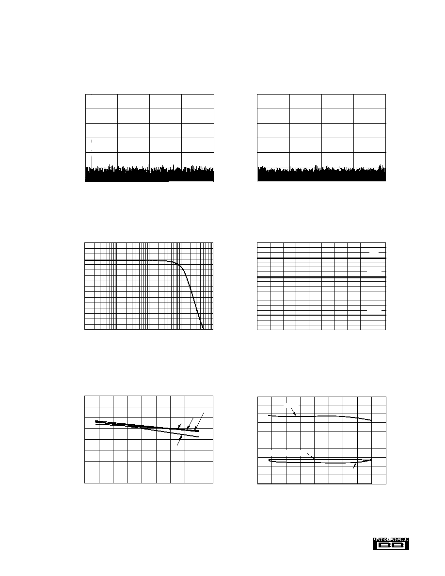
TYPICAL PERFORMANCE CURVES
T
A
= +25
∞
C, f
S
= 40kHz, V
DIG
= V
ANA
= +5V, using internal reference and fixed resistors shown in Figure 7b, unless otherwise specified.
FREQUENCY SPECTRUM
(8192 Point FFT; f
IN
= 1kHz, 0dB)
Frequency (kHz)
Amplitude (dB)
0
≠20
≠40
≠60
≠80
≠100
≠120
0
5
10
15
20
SIGNAL-TO-(NOISE + DISTORTION)
vs INPUT FREQUENCY (f
IN
= 0dB)
90
80
70
60
50
40
30
20
10
SINAD (dB)
100
1k
10k
100k
1M
Input Signal Frequency (Hz)
10kHz
20kHz
30kHz
40kHz
SIGNAL-TO-(NOISE + DISTORTION) vs TEMPERATURE
(f
IN
= 1kHz, 0dB; f
S
= 10kHz to 40kHz)
74.0
73.9
73.8
73.7
73.6
≠75
≠50
≠25
0
25
50
75
100
125
150
Temperature (∞C)
SINAD (dB)
A.C. PARAMETERS vs TEMPERATURE
(f
IN
= 1kHz, 0dB)
110
105
100
95
90
85
80
75
70
65
60
≠60
≠65
≠70
≠75
≠80
≠85
≠90
≠95
≠100
≠105
≠110
SFDR, SNR, and SINAD (dB)
THD (dB)
≠75
≠50
≠25
0
25
50
75
100
125
150
Temperature (∞C)
SFDR
SNR and SINAD
THD
FREQUENCY SPECTRUM
(8192 Point FFT; f
IN
= 15kHz, 0dB)
Frequency (kHz)
Amplitude (dB)
0
≠20
≠40
≠60
≠80
≠100
≠120
0
5
10
15
20
SIGNAL-TO-(NOISE + DISTORTION)
vs INPUT FREQUENCY AND INPUT AMPLITUDE
90
80
70
60
50
40
30
20
10
0
SINAD (dB)
0
2
4
6
8
10
12
14
16
18
20
Input Signal Frequency (kHz)
0dB
≠20dB
≠60dB

6
Æ
ADS7806
3
2
1
0
≠1
≠2
TYPICAL PERFORMANCE CURVES
(CONT)
T
A
= +25
∞
C, f
S
= 40kHz, V
DIG
= V
ANA
= +5V, using internal reference and fixed resistors shown in Figure 7b, unless otherwise specified.
0.10
0
≠0.10
12-Bit LSBs
0
4095
3584
3072
2560
2048
1536
1024
512
Decimal Code
0.10
0
≠0.10
12-Bit LSBs
0
4095
3584
3072
2560
2048
1536
1024
512
Decimal Code
All Codes DNL
3
2
1
0
≠1
≠2
0.20
0
≠0.20
Percent
From Ideal
mV From Ideal
ENDPOINT ERRORS (20V BIPOLAR RANGE)
Temperature (
∞
C)
≠50
≠25
0
25
50
75
100
125
150
≠75
Percent
From Ideal
0.20
0
≠0.20
0.40
0.20
0
0.40
0.20
0
Percent
From Ideal
mV From Ideal
ENDPOINT ERRORS (UNIPOLAR RANGES)
Temperature (
∞
C)
≠75
≠50
≠25
0
25
50
75
100
125
150
Percent
From Ideal
All Codes INL
UPO Error
+F
S
Error (4V Range)
+F
S
Error (5V Range)
≠F
S
Error
+F
S
Error
BPZ Error
POWER SUPPLY RIPPLE SENSITIVITY
INL/DNL DEGRADATION PER LSB OF P-P RIPPLE
Power Supply Ripple Frequency (Hz)
10
1
10
2
10
3
10
4
10
5
10
6
10
7
1
10
≠1
10
≠2
10
≠3
10
≠4
10
≠5
Linearity Degradation (LSB/LSB)
INL
DNL
INTERNAL REFERENCE VOLTAGE vs TEMPERATURE
≠75
≠50
≠25
0
25
50
75
100
125
150
2.520
2.515
2.510
2.505
2.500
2.495
2.490
2.485
2.480
Internal Reference (V)
Temperature (∞C)
CONVERSION TIME vs TEMPERATURE
15.10
15.00
14.90
14.80
14.70
14.60
14.50
14.40
14.30
14.20
≠75
≠50
≠25
0
25
50
75
100
125
150
Temperature (∞C)
Conversion Time (
µ
s)

7
Æ
ADS7806
BASIC OPERATION
PARALLEL OUTPUT
Figure 1a) shows a basic circuit to operate the ADS7806
with a
±
10V input range and parallel output. Taking R/C
(pin 22) LOW for 40ns (12
µ
s max) will initiate a conver-
sion. BUSY (pin 24) will go LOW and stay LOW until the
conversion is completed and the output register is updated.
If BYTE (pin 21) is LOW, the 8 most significant bits will be
valid when BUSY rises; if BYTE is HIGH, the 4 least
significant bits will be valid when BUSY rises. Data will be
output in Binary Two's Complement format. BUSY going
HIGH can be used to latch the data. After the first byte has
been read, BYTE can be toggled allowing the remaining
byte to be read. All convert commands will be ignored while
BUSY is LOW.
The ADS7806 will begin tracking the input signal at the end
of the conversion. Allowing 25
µ
s between convert com-
mands assures accurate acquisition of a new signal.
The offset and gain are adjusted internally to allow external
trimming with a single supply. The external resistors com-
pensate for this adjustment and can be left out if the offset
and gain will be corrected in software (refer to the Calibra-
tion section).
SERIAL OUTPUT
Figure 1b) shows a basic circuit to operate the ADS7806
with a
±
10V input range and serial output. Taking R/C (pin
22) LOW for 40ns (12
µ
s max) will initiate a conversion and
output valid data from the previous conversion on SDATA
(pin 19) synchronized to 12 clock pulses output on
DATACLK (pin 18). BUSY (pin 24) will go LOW and stay
LOW until the conversion is completed and the serial data
has been transmitted. Data will be output in Binary Two's
Complement format, MSB first, and will be valid on both the
rising and falling edges of the data clock. BUSY going
HIGH can be used to latch the data. All convert commands
will be ignored while BUSY is LOW.
The ADS7806 will begin tracking the input signal at the end
of the conversion. Allowing 25
µ
s between convert com-
mands assures accurate acquisition of a new signal.
The offset and gain are adjusted internally to allow external
trimming with a single supply. The external resistors com-
pensate for this adjustment and can be left out if the offset
and gain will be corrected in software (refer to the Calibra-
tion section).
STARTING A CONVERSION
The combination of CS (pin 23) and R/C (pin 22) LOW for
a minimum of 40ns immediately puts the sample/hold of the
ADS7806 in the hold state and starts conversion `n'. BUSY
(pin 24) will go LOW and stay LOW until conversion `n' is
completed and the internal output register has been updated.
All new convert commands during BUSY LOW will be
ignored. CS and/or R/C must go HIGH before BUSY goes
HIGH or a new conversion will be initiated without suffi-
cient time to acquire a new signal.
FIGURE 1a. Basic
±
10V Operation, both Parallel and Serial
Output.
FIGURE 1b. Basic
±
10V Operation with Serial Output.
1
2
3
4
5
6
7
8
9
10
11
12
13
14
28
27
26
25
24
23
22
21
20
19
18
17
16
15
ADS7806
Parallel Output
200
66.5k
±10V
+5V
0.1µF
NC
(1)
10µF
+
+5V
+
100
B6
B5
B4
LOW LOW LOW
B9
B8
B11
(MSB)
Pin 21
LOW
B10
B7
B1
B0
B3
Pin 21
HIGH
NOTE: (1) SDATA (pin 19) is always active.
B2
LOW
(LSB)
2.2µF
+
+
2.2µF
Convert Pulse
BUSY
R/C
BYTE
40ns min
1
2
3
4
5
6
7
8
9
10
11
12
13
14
NC
(1)
NC
(1)
NC
(1)
NC
(1)
NC
(1)
28
27
26
25
24
23
22
21
20
19
18
17
16
15
ADS7806
Serial Output
200
66.5k
±10V
+5V
0.1µF
NC
(1)
NC
(1)
NC
(1)
10µF
+
+5V
+
100
+
+
2.2µF
2.2µF
Convert Pulse
BUSY
40ns min
NOTE: (1) These pins should be left
unconnected.They will be active when
R/C is HIGH.
R/C
SDATA
DATACLK

8
Æ
ADS7806
CS
R/C
BUSY
OPERATION
1
X
X
None. Databus is in Hi-Z state.
0
1
Initiates conversion "n". Databus remains
in Hi-Z state.
0
1
Initiates conversion "n". Databus enters Hi-Z
state.
0
1
Conversion "n" completed. Valid data from
conversion "n" on the databus.
1
1
Enables databus with valid data from
conversion "n".
1
0
Enables databus with valid data from
conversion "n-1"
(1)
. Conversion n in progress.
0
0
Enables databus with valid data from
conversion "n-1"
(1)
. Conversion "n" in progress.
0
0
New conversion initiated without acquisition
of a new signal. Data will be invalid. CS and/or
R/C must be HIGH when BUSY goes HIGH.
X
X
0
New convert commands ignored. Conversion
"n" in progress.
NOTE: (1) See Figures 2 and 3 for constraints on data valid from
conversion "n-1".
The ADS7806 will begin tracking the input signal at the end
of the conversion. Allowing 25
µ
s between convert com-
mands assures accurate acquisition of a new signal. Refer to
Tables III and IV for a summary of CS, R/C, and BUSY
states and Figures 2 through 6 for timing diagrams.
CS and R/C are internally OR'd and level triggered. There
is not a requirement which input goes LOW first when
initiating a conversion. If, however, it is critical that CS or
R/C initiates conversion `n', be sure the less critical input is
LOW at least 10ns prior to the initiating input. If EXT/INT
(pin 8) is LOW when initiating conversion `n', serial data
from conversion `n-1' will be output on SDATA (pin 19)
following the start of conversion `n'. See Internal Data
Clock in the Reading Data section.
To reduce the number of control pins, CS can be tied LOW
using R/C to control the read and convert modes. This will
have no effect when using the internal data clock in the serial
output mode. However, the parallel output and the serial
output (only when using an external data clock) will be
affected whenever R/C goes HIGH. Refer to the Reading
Data section.
READING DATA
The ADS7806 outputs serial or parallel data in Straight
Binary or Binary Two's Complement data output format. If
SB/BTC (pin 7) is HIGH, the output will be in SB format,
and if LOW, the output will be in BTC format. Refer to
Table V for ideal output codes.
The parallel output can be read without affecting the internal
output registers; however, reading the data through the serial
Table III. Control Functions When Using Parallel Output
(DATACLK tied LOW, EXT/INT tied HIGH).
CS
R/C
BUSY
EXT/INT
DATACLK
OPERATION
0
1
0
Output
Initiates conversion "n". Valid data from conversion "n-1" clocked out on SDATA.
0
1
0
Output
Initiates conversion "n". Valid data from conversion "n-1" clocked out on SDATA.
0
1
1
Input
Initiates conversion "n". Internal clock still runs conversion process.
0
1
1
Input
Initiates conversion "n". Internal clock still runs conversion process.
1
1
1
Input
Conversion "n" completed. Valid data from conversion "n" clocked out on SDATA synchronized
to external data clock.
1
0
1
Input
Valid data from conversion "n-1" output on SDATA synchronized to external data clock.
Conversion "n" in progress.
0
0
1
Input
Valid data from conversion "n-1" output on SDATA synchronized to external data clock.
Conversion "n" in progress.
0
0
X
X
New conversion initiated without acquisition of a new signal. Data will be invalid. CS and/or R/C
must be HIGH when BUSY goes HIGH.
X
X
0
X
X
New convert commands ignored. Conversion "n" in progress.
NOTE: (1) See Figures 4, 5, and 6 for constraints on data valid from conversion "n-1".
Table IV. Control Functions When Using Serial Output.
HEX
HEX
BINARY CODE
CODE
BINARY CODE
CODE
+Full Scale (FS ≠ 1LSB)
9.99512V
4.99878V
3.999024V
0111 1111 1111 1111
7FF
1111 1111 1111 1111
FFF
Midscale
0V
2.5V
2V
0000 0000 0000 0000
000
1000 0000 0000 0000
800
One LSB Below Midscale
≠4.88mV
2.49878V
1.999024V
1111 1111 1111 1111
FFF
0111 1111 1111 1111
7FF
≠Full Scale
≠10V
0V
0V
1000 0000 0000 0000
800
0000 0000 0000 0000
000
DESCRIPTION
ANALOG INPUT
Full-Scale Range
±
10
0V to 5V
0V to 4V
Least Significant Bit (LSB)
4.88mV
1.22mV
976
µ
V
Table V. Output Codes and Ideal Input Voltages.
BINARY TWO'S COMPLEMENT
STRAIGHT BINARY
(SB/BTC LOW)
(SB/BTC HIGH)
DIGITAL OUTPUT

9
Æ
ADS7806
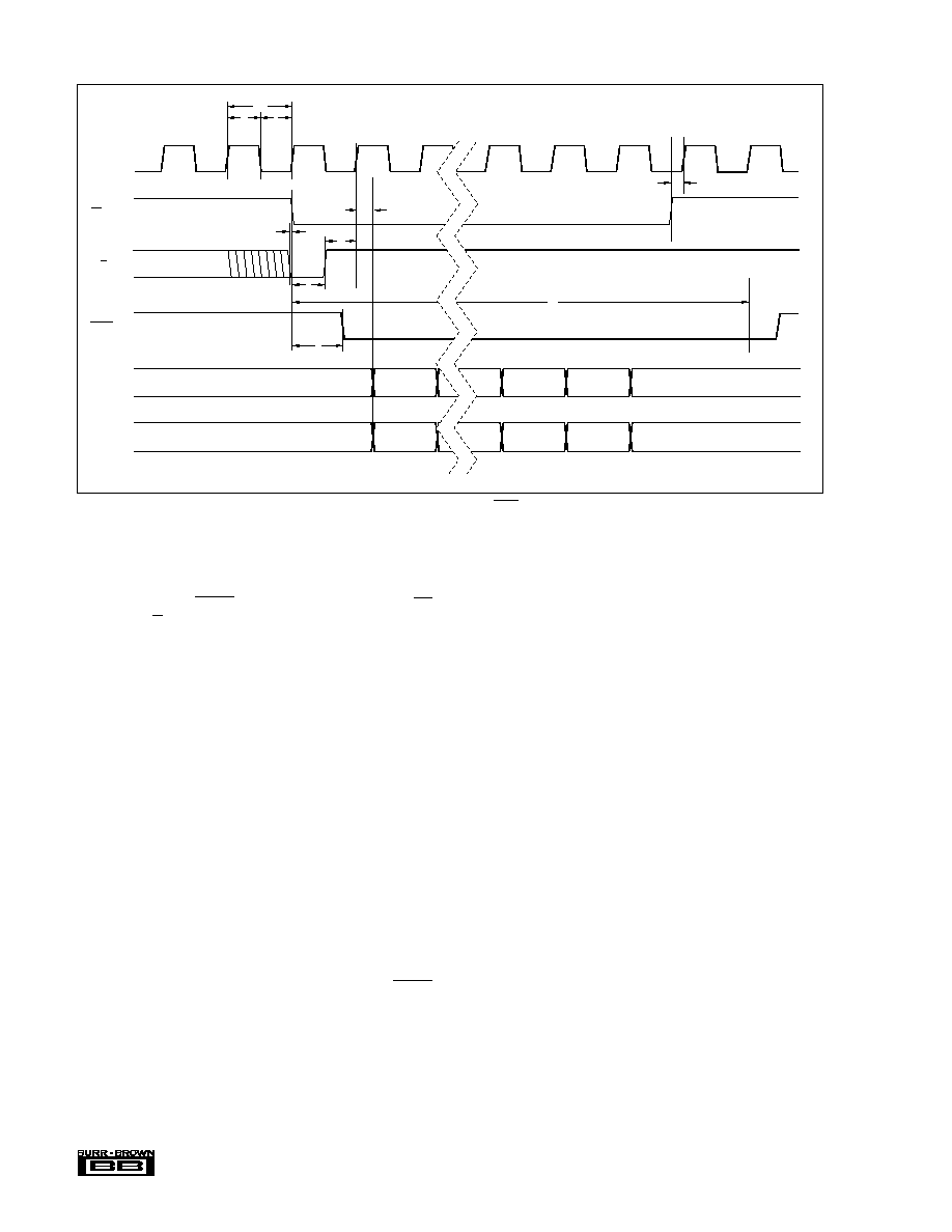
PARALLEL OUTPUT (After a Conversion)
After conversion `n' is completed and the output registers
have been updated, BUSY (pin 24) will go HIGH. Valid data
from conversion `n' will be available on D7-D0 (pins 9-13
and 15-17). BUSY going high can be used to latch the data.
Refer to Table VI and Figures 2 and 3 for timing constraints.
PARALLEL OUTPUT (During a Conversion)
After conversion `n' has been initiated, valid data from
conversion `n-1' can be read and will be valid up to 12
µ
s
after the start of conversion `n'. Do not attempt to read data
beyond 12
µ
s after the start of conversion `n' until BUSY
(pin 24) goes HIGH; this may result in reading invalid data.
Refer to Table VI and Figures 2 and 3 for timing constraints.
port will shift the internal output registers one bit per data
clock pulse. As a result, data can be read on the parallel port
prior to reading the same data on the serial port, but data
cannot be read through the serial port prior to reading the
same data on the parallel port.
PARALLEL OUTPUT
To use the parallel output, tie EXT/INT (pin 8) HIGH and
DATACLK (pin 18) LOW. SDATA (pin 19) should be left
unconnected. The parallel output will be active when R/C
(pin 22) is HIGH and CS (pin 23) is LOW. Any other
combination of CS and R/C will tri-state the parallel output.
Valid conversion data can be read in two 8-bit bytes on D7-
D0 (pins 9-13 and 15-17) . When BYTE (pin 21) is LOW,
the 8 most significant bits will be valid with the MSB on D7.
When BYTE is HIGH, the 4 least significant bits will be
valid with the LSB on D4. BYTE can be toggled to read both
bytes within one conversion cycle.
Upon initial power up, the parallel output will contain
indeterminate data.
t
10
BUSY
R/C
MODE
Acquire
Convert
t
11
t
7
t
6
t
3
t
4
t
1
Acquire
Convert
t
8
t
6
t
3
Parallel
Data Bus
Previous
High Byte Valid
t
12
Hi-Z
Not Valid
t
2
t
9
High Byte
Valid
t
12
t
9
t
12
BYTE
t
1
Previous Low
Byte Valid
Previous High
Byte Valid
Low Byte
Valid
High Byte
Valid
t
12
Hi-Z
t
12
t
12
t
5
Hi-Z State
BUSY
R/C
DATA
BUS
High Byte
t
3
t
4
t
21
t
21
t
1
t
21
t
21
BYTE
t
21
t
21
t
21
t
21
t
21
t
21
Hi-Z State
Low Byte
Hi-Z State
t
9
t
12
t
9
t
12
CS
FIGURE 2. Conversion Timing with Parallel Output (CS and DATACLK tied LOW, EXT/INT tied HIGH).
FIGURE 3. Using CS to Control Conversion and Read Timing with Parallel Outputs.

10
Æ
ADS7806
SERIAL OUTPUT
Data can be clocked out with the internal data clock or an
external data clock. When using serial output, be careful
with the parallel outputs, D7-D0 (pins 9-13 and 15-17), as
these pins will come out of Hi-Z state whenever CS (pin 23)
is LOW and R/C (pin 22) is HIGH. The serial output can not
be tri-stated and is always active.
FIGURE 4. Serial Data Timing Using Internal Data Clock (TAG tied LOW).
TABLE VI. Conversion and Data Timing. T
A
= ≠40
∞
C to
+85
∞
C.
INTERNAL DATA CLOCK (During A Conversion)
To use the internal data clock, tie EXT/INT (pin 8) LOW.
The combination of R/C (pin 22) and CS (pin 23) LOW will
initiate conversion `n' and activate the internal data clock
(typically 900kHz clock rate). The ADS7806 will output 12
bits of valid data, MSB first, from conversion `n-1' on
SDATA (pin 19), synchronized to 12 clock pulses output on
DATACLK (pin 18). The data will be valid on both the
rising and falling edges of the internal data clock. The rising
edge of BUSY (pin 24) can be used to latch the data. After
the 12th clock pulse, DATACLK will remain LOW until the
next conversion is initiated, while SDATA will go to what-
ever logic level was input on TAG (pin 20) during the first
clock pulse. Refer to Table VI and Figure 4.
EXTERNAL DATA CLOCK
To use an external data clock, tie EXT/INT (pin 8) HIGH. The
external data clock is not a conversion clock; it can only be
used as a data clock. To enable the output mode of the
ADS7806, CS (pin 23) must be LOW and R/C (pin 22) must
be HIGH. DATACLK must be HIGH for 20% to 70% of the
total data clock period; the clock rate can be between DC and
10MHz. Serial data from conversion `n' can be output on
SDATA (pin 19) after conversion `n' is completed or during
conversion `n + 1'.
An obvious way to simplify control of the converter is to tie
CS LOW and use R/C to initiate conversions. While this is
perfectly acceptable, there is a possible problem when using
an external data clock. At an indeterminate point from 12
µ
s
after the start of conversion 'n' until BUSY rises, the internal
logic will shift the results of conversion 'n' into the output
register. If CS is LOW, R/C is HIGH, and the external clock
is HIGH at this point, data will be lost. So, with CS LOW,
either R/C and/or DATACLK must be LOW during this
period to avoid losing valid data.
SYMBOL
DESCRIPTION
MIN
TYP MAX UNITS
t
1
Convert Pulse Width
0.04
12
µ
s
t
2
Data Valid Delay after R/C LOW
14.7
20
µ
s
t
3
BUSY Delay from
85
ns
Start of Conversion
t
4
BUSY LOW
14.7
20
µ
s
t
5
BUSY Delay after
90
ns
End of Conversion
t
6
Aperture Delay
40
ns
t
7
Conversion Time
14.7
20
µ
s
t
8
Acquisition Time
5
µ
s
t
9
Bus Relinquish Time
10
83
ns
t
10
BUSY Delay after Data Valid
20
60
ns
t
11
Previous Data Valid
12
14.7
µ
s
after Start of Conversion
t
12
Bus Access Time and BYTE Delay
83
ns
t
13
Start of Conversion
1.4
µ
s
to DATACLK Delay
t
14
DATACLK Period
1.1
µ
s
t
15
Data Valid to DATACLK
20
75
ns
HIGH Delay
t
16
Data Valid after DATACLK
400
600
ns
LOW Delay
t
17
External DATACLK Period
100
ns
t
18
External DATACLK LOW
40
ns
t
19
External DATACLK HIGH
50
ns
t
20
CS and R/C to External
25
ns
DATACLK Setup Time
t
21
R/C to CS Setup Time
10
ns
t
22
Valid Data after DATACLK HIGH
25
ns
t
7
+ t
8
Throughput Time
25
µ
s
1
MSB Valid
CS or R/C
(1)
DATACLK
SDATA
BUSY
t
7
+ t
8
t
16
t
15
t
14
t
13
2
3
11
12
Bit 10 Valid
Bit 1 Valid
Bit 9 Valid
LSB Valid
NOTE: (1) If controlling with CS, tie R/C LOW. Data bus pins will remain Hi-Z at all times.
If controlling with R/C, tie CS LOW. Data bus pins will be active when R/C is HIGH, and should be left unconnected.
1
MSB Valid
2
Bit 10 Valid
(Results from previous conversion.)

11
Æ
ADS7806
FIGURE 5. Conversion and Read Timing with External Clock (EXT/INT Tied HIGH) Read after Conversion.
EXTERNAL
DATACLK
CS
0
Bit 11 (MSB)
R/C
BUSY
SDATA
TAG
12
3
1
1
1
2
1
3
1
4
Bit 10
Bit 1
Bit 0 (LSB)
Tag 0
Tag 1
Tag 1
Tag 2
Tag 11
Tag 12
Tag 13
Tag 14
Tag 0
t
20
t
21
t
21
t
3
t
17
t
18
t
19
t
20
t
22
t
1
12
Æ
ADS7806
FIGURE 6. Conversion and Read Timing with External Clock (EXT/INT tied HIGH) Read During a Conversion.
EXTERNAL DATA CLOCK
(After a Conversion)
After conversion `n' is completed and the output registers
have been updated, BUSY (pin 24) will go HIGH. With CS
LOW and R/C HIGH, valid data from conversion `n' will be
output on SDATA (pin 19) synchronized to the external data
clock input on DATACLK (pin 18). The MSB will be valid
on the first falling edge and the second rising edge of the
external data clock. The LSB will be valid on the 12th falling
edge and 13th rising edge of the data clock. TAG (pin 20)
will input a bit of data for every external clock pulse. The
first bit input on TAG will be valid on SDATA on the 13th
falling edge and the 14th rising edge of DATACLK; the
second input bit will be valid on the 14th falling edge and the
15th rising edge, etc. With a continuous data clock, TAG
data will be output on SDATA until the internal output
registers are updated with the results from the next conver-
sion. Refer to Table VI and Figure 5.
EXTERNAL DATA CLOCK
(During a Conversion)
After conversion `n' has been initiated, valid data from
conversion `n-1' can be read and will be valid up to 12
µ
s
after the start of conversion `n'. Do not attempt to clock out
data from 12
µ
s after the start of conversion `n' until BUSY
(pin 24) rises; this will result in data loss. NOTE: For the
best possible performance when using an external data
clock, data should not be clocked out during a conversion.
The switching noise of the asynchronous data clock can
cause digital feedthrough degrading the converter's perfor-
mance. Refer to Table VI and Figure 6.
TAG FEATURE
TAG (Pin 20) inputs serial data synchronized to the external
or internal data clock.
When using an external data clock, the serial bit stream input
on TAG will follow the LSB output on SDATA until the
internal output register is updated with new conversion
results. See Table VI and Figures 5 and 6.
The logic level input on TAG for the first rising edge of the
internal data clock will be valid on SDATA after all 12 bits
of valid data have been output.
INPUT RANGES
The ADS7806 offers three input ranges: standard
±
10V and
0-5V, and a 0-4V range for complete, single supply systems.
Figures 7a and 7b show the necessary circuit connections for
implementing each input range and optional offset and gain
adjust circuitry. Offset and full scale error
(1)
specifications
are tested and guaranteed with the fixed resistors shown in
Figure 7b. Adjustments for offset and gain are described in
the Calibration section of this data sheet.
The offset and gain are adjusted internally to allow external
trimming with a single supply. The external resistors com-
pensate for this adjustment and can be left out if the offset
and gain will be corrected in software (refer to the Calibra-
tion section).
The input impedance, summarized in Table II, results from the
combination of the internal resistor network shown on the
front page of the product data sheet and the external resistors
NOTE: (1) Full scale error includes offset and gain errors measured at both
+FS and ≠FS.
EXTERNAL
DATACLK
CS
Bit 11 (MSB)
R/C
BUSY
DATA
TAG
Bit 0 (LSB)
Tag 0
Tag 1
Tag 1
Tag 12
Tag 13
Tag 14
Tag 0
t
20
t
21
t
1
t
11
t
3
t
17
t
18
t
19
t
22
t
20

13
Æ
ADS7806
OFFSET ADJUST
GAIN ADJUST
INPUT RANGE
RANGE (mV)
RANGE (mV)
±
10V
±
15
±
60
0 to 5V
±
4
±
30
0 to 4V
±
3
±
30
TABLE VII. Offset and Gain Adjust Ranges for Hardware
Calibration (see Figure 7a).
±
10V
0-5V
0-4V
200
1
2
3
4
5
6
AGND2
REF
CAP
R2
IN
AGND1
R1
IN
+
+
2.2µF
2.2µF
100
+5V
66.5k
V
IN
200
1
2
3
4
5
6
AGND2
REF
CAP
R2
IN
AGND1
R1
IN
+
+
2.2µF
2.2µF
33.2k
100
V
IN
FIGURE 7b. Circuit Diagrams (Without Hardware Trim).
±
10V
0-5V
0-4V
FIGURE 7a. Circuit Diagrams (With Hardware Trim).
200
1
2
3
4
5
6
AGND2
REF
CAP
R2
IN
AGND1
R1
IN
+
+
2.2µF
2.2µF
33.2k
100
V
IN
1M
+5V
50k
50k
200
1
2
3
4
5
6
AGND2
REF
CAP
R2
IN
AGND1
R1
IN
+
+
2.2µF
2.2µF
1M
+5V
50k
50k
33.2k
100
V
IN
200
1
2
3
4
5
6
AGND2
REF
CAP
R2
IN
AGND1
R1
IN
+
+
2.2µF
2.2µF
1M
+5V
50k
+5V
100
33.2k
50k
V
IN
used for each input range (see Figure 8). The input resistor
divider network provides inherent overvoltage protection
guaranteed to at least
±
25V.
Analog inputs above or below the expected range will yield
either positive full scale or negative full scale digital outputs
respectively. There will be no wrapping or folding over for
analog inputs outside the nominal range.
CALIBRATION
HARDWARE CALIBRATION
To calibrate the offset and gain of the ADS7806 in hard-
ware, install the resistors shown in Figure 7a. Table VII lists
the hardware trim ranges relative to the input for each input
range.
SOFTWARE CALIBRATION
To calibrate the offset and gain in software, no external
resistors are required. However, to get the data sheet speci-
fications for offset and gain, the resistors shown in Figure 7b
are necessary. See the No Calibration section for more
details on the external resistors. Refer to Table VIII for the
range of offset and gain errors with and without the external
resistors.
NO CALIBRATION
See Figure 7b for circuit connections. Note that the actual
voltage dropped across the external resistors is at least two
orders of magnitude lower than the voltage dropped across
the internal resistor divider network. This should be consid-
200
1
2
3
4
5
6
AGND2
REF
CAP
R2
IN
AGND1
R1
IN
+
+
2.2µF
2.2µF
33.2k
100
V
IN
14
Æ
ADS7806
ered when choosing the accuracy and drift specifications of
the external resistors. In most applications, 1% metal-film
resistors will be sufficient.
The external resistors shown in Figure 7b may not be
necessary in some applications. These resistors provide
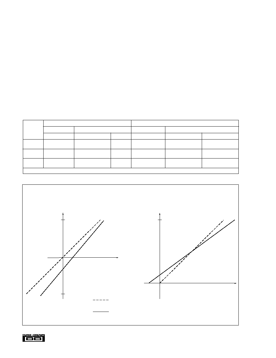
compensation for an internal adjustment of the offset and
gain which allows calibration with a single supply. Not
using the external resistors will result in offset and gain
errors in addition to those listed in the electrical specifica-
tions section. Offset refers to the equivalent voltage of the
digital output when converting with the input grounded. A
positive gain error occurs when the equivalent output volt-
age of the digital output is larger than the analog input. Refer
to Table VIII for nominal ranges of gain and offset errors
with and without the external resistors. Refer to Figure 8 for
typical shifts in the transfer functions which occur when the
external resistors are removed.
To further analyze the effects of removing any combination
of the external resistors, consider Figure 9. The combination
of the external and the internal resistors form a voltage
divider which reduces the input signal to a 0.3125V to
2.8125V input range at the CDAC. The internal resistors are
laser trimmed to high relative accuracy to meet full specifi-
cations. The actual input impedance of the internal resistor
network looking into pin 1 or pin 3 however, is only accurate
to
±
20% due to process variations. This should be taken into
account when determining the effects of removing the exter-
nal resistors.
REFERENCE
The ADS7806 can operate with its internal 2.5V reference or
an external reference. By applying an external reference to
INPUT
RANGE
W/ RESISTORS
W/OUT RESISTORS
W/ RESISTORS
W/OUT RESISTORS
(V)
RANGE (mV)
RANGE (mV)
TYP (mV)
RANGE (% FS)
RANGE (% FS)
TYP
±
10
≠10
BPZ
10
0
BPZ
35
+15
≠0.4
G
0.4
≠0.3
G
0.5
+0.05
0.15
G
(1)
0.15
≠0.1
G
(1)
0.2
+0.05
0 to 5
≠3
UPO
3
≠12
UPO
≠3
≠7.5
≠0.4
G
0.4
≠1.0
G
0.1
≠0.2
0.15
G
(1)
0.15
≠0.55
G
(1)
≠0.05
≠0.2
0 to 4
≠3
UPO
3
≠10.5
UPO
≠1.5
≠6
≠0.4
G
0.4
≠1.0
G
0.1
≠0.2
≠0.15
G
(1)
0.15
≠0.55
G
(1)
≠0.05
≠0.2
Note: (1) High Grade.
OFFSET ERROR
GAIN ERROR
TABLE VIII. Range of Offset and Gain Errors with and without External Resistors
Digital Output
(b) Unipolar
≠Full Scale
+Full Scale
Analog Input
Digital Output
(a) Bipolar
≠Full Scale
+Full Scale
Analog Input
Typical Transfer Functions
With External Resistors
Typical Transfer Functions
Without External Resistors
FIGURE 8. Typical Transfer Functions With and Without External Resistors.

15
Æ
ADS7806
CAP
CAP (pin 4) is the output of the internal reference buffer. A
2.2
µ
F tantalum capacitor should be placed as close as
possible to the CAP pin from ground to provide optimum
switching currents for the CDAC throughout the conversion
cycle. This capacitor also provides compensation for the
FIGURE 10. Characteristic Impedances of Internal Buffer.
PWRD 0
PWRD 0
PWRD 1
PWRD 1
REFD 0
REFD 1
REFD 0
REFD 1
Z
CAP
(
)
1
1
200
200
Z
REF
(
)
6k
100M
6k
100M
CDAC
CAP
(Pin 4)
Z
CAP
Buffer
Internal
Reference
REF
(Pin 5)
Z
REF
FIGURE 9. Circuit Diagrams Showing External and Internal Resistors.
pin 5, the internal reference can be bypassed; REFD (pin 26)
tied HIGH will power-down the internal reference reducing
the overall power consumption of the ADS7806 by approxi-
mately 5mW.
The internal reference has approximately an 8 ppm/
∞
C drift
(typical) and accounts for approximately 20% of the full
scale error (FSE =
±
0.5% for low grade,
±
0.25% for high
grade).
The ADS7806 also has an internal buffer for the reference
voltage. See Figure 10 for characteristic impedances at the
input and output of the buffer with all combinations of
power down and reference down.
REF
REF (pin 5) is an input for an external reference or the output
for the internal 2.5V reference. A 2.2
µ
F tantalum capacitor
should be connected as close as possible to the REF pin from
ground. This capacitor and the output resistance of REF
create a low pass filter to bandlimit noise on the reference.
Using a smaller value capacitor will introduce more noise to
the reference, degrading the SNR and SINAD. The REF pin
should not be used to drive external AC or DC loads. See
Figure 10.
The range for the external reference is 2.3V to 2.7V and
determines the actual LSB size. Increasing the reference
voltage will increase the full scale range and the LSB size of
the converter which can improve the SNR.
39.8k
200
V
IN
CDAC (High Impedance)
(0.3125V to 2.8125V)
+5V
9.9k
100
20k
40k
+2.5V
66.5k
+2.5V
39.8k
200
CDAC (High Impedance)
(0.3125V to 2.8125V)
V
IN
9.9k
33.2k
20k
40k
+2.5V
100
+2.5V
39.8k
200
V
IN
CDAC (High Impedance)
(0.3125V to 2.8125V)
9.9k
33.2k
20k
40k
+2.5V
100
+2.5V

16
Æ
ADS7806
output of the buffer. Using a capacitor any smaller than 1
µ
F
can cause the output buffer to oscillate and may not have
sufficient charge for the CDAC. Capacitor values larger than
2.2
µ
F will have little affect on improving performance. See
Figures 10 and 11.
The output of the buffer is capable of driving up to 1mA of
current to a DC load. Using an external buffer will allow the
internal reference to be used for larger DC loads and AC
loads. Do not attempt to directly drive an AC load with the
output voltage on CAP. This will cause performance degra-
dation of the converter.
REFERENCE
AND POWER DOWN
The ADS7806 has analog power down and reference power
down capabilities via PWRD (pin 25) and REFD (pin 26)
respectively. PWRD and REFD HIGH will power down all
analog circuitry maintaining data from the previous conver-
sion in the internal registers, provided that the data has not
already been shifted out through the serial port. Typical
power consumption in this mode is 50
µ
W. Power recovery
is typically 1ms, using a 2.2
µ
F capacitor connected to CAP.
See Figure 11 for power-down to power-up recovery time
relative to the capacitor value on CAP. With +5V applied to
V
DIG
, the digital circuitry of the ADS7806 remains active at
all times, regardless of PWRD and REFD states.
PWRD
PWRD HIGH will power down all of the analog circuitry
except for the reference. Data from the previous conversion
will be maintained in the internal registers and can still be
read. With PWRD HIGH, a convert command yields mean-
ingless data.
REFD
REFD HIGH will power down the internal 2.5V reference.
All other analog circuitry, including the reference buffer,
will be active. REFD should be HIGH when using an
external reference to minimize power consumption and the
loading effects on the external reference. See Figure 10 for
the characteristic impedance of the reference buffer's input
for both REFD HIGH and LOW. The internal reference
consumes approximately 5mW.
LAYOUT
POWER
For optimum performance, tie the analog and digital power
pins to the same +5V power supply and tie the analog and
digital grounds together. As noted in the electrical specifica-
tions, the ADS7806 uses 90% of its power for the analog
circuitry. The ADS7806 should be considered as an analog
component.
The +5V power for the A/D should be separate from the +5V
used for the system's digital logic. Connecting V
DIG
(pin 28)
directly to a digital supply can reduce converter performance
due to switching noise from the digital logic. For best
performance, the +5V supply can be produced from what-
ever analog supply is used for the rest of the analog signal
conditioning. If +12V or +15V supplies are present, a simple
+5V regulator can be used. Although it is not suggested, if
the digital supply must be used to power the converter, be
sure to properly filter the supply. Either using a filtered
digital supply or a regulated analog supply, both V
DIG
and
V
ANA
should be tied to the same +5V source.
GROUNDING
Three ground pins are present on the ADS7806. D
GND
is the
digital supply ground. A
GND2
is the analog supply ground.
A
GND1
is the ground to which all analog signals internal to
the A/D are referenced. A
GND1
is more susceptible to current
induced voltage drops and must have the path of least
resistance back to the power supply.
All the ground pins of the A/D should be tied to an analog
ground plane, separated from the system's digital logic
ground, to achieve optimum performance. Both analog and
digital ground planes should be tied to the "system" ground
as near to the power supplies as possible. This helps to
prevent dynamic digital ground currents from modulating
the analog ground through a common impedance to power
ground.
SIGNAL CONDITIONING
The FET switches used for the sample hold on many CMOS
A/D converters release a significant amount of charge injec-
tion which can cause the driving op amp to oscillate. The
amount of charge injection due to the sampling FET switch
on the ADS7806 is approximately 5-10% of the amount on
similar ADCs with the charge redistribution DAC (CDAC)
architecture. There is also a resistive front end which attenu-
ates any charge which is released. The end result is a
minimal requirement for the drive capability on the signal
conditioning preceding the A/D. Any op amp sufficient for
the signal in an application will be sufficient to drive the
ADS7806.
FIGURE 11. Power-Down to Power-Up Time vs Capacitor
Value on CAP.
"CAP" Pin Value (µF)
0.1
1
10
100
7000
5000
6000
4000
3000
2000
1000
0
µs

17
Æ
ADS7806
The resistive front end of the ADS7806 also provides a
guaranteed
±
25V overvoltage protection. In most cases, this
eliminates the need for external over voltage protection
circuitry.
INTERMEDIATE LATCHES
The ADS7806 does have tri-state outputs for the parallel
port, but intermediate latches should be used if the bus will
be active during conversions. If the bus is not active during
conversion, the tri-state outputs can be used to isolate the
A/D from other peripherals on the same bus.
Intermediate latches are beneficial on any monolithic A/D
converter. The ADS7806 has an internal LSB size of 610
µ
V.
Transients from fast switching signals on the parallel port,
even when the A/D is tri-stated, can be coupled through the
substrate to the analog circuitry causing degradation of
converter performance. The effects of this phenomenon will
be more obvious when using the pin-compatible ADS7807
or any of the other 16-bit converters in the ADS Family. This
is due to the smaller internal LSB size of 38
µ
V.
APPLICATIONS INFORMATION
QSPI INTERFACING
Figure 12 shows a simple interface between the ADS7806
and any QSPI equipped microcontroller. This interface as-
sumes that the convert pulse does not originate from the
microcontroller and that the ADS7806 is the only serial
peripheral.
Before enabling the QSPI interface, the microcontroller
must be configured to monitor the slave select line. When a
transition from LOW to HIGH occurs on Slave Select (SS)
from BUSY (indicating the end of the current conversion),
the port can be enabled. If this is not done, the microcontroller
and the and the A/D may be "out-of-sync."
Figure 13 shows another interface between the ADS7806
and a QSPI equipped microcontroller. The interface allows
the microcontroller to give the convert pulses while also
allowing multiple peripherals to be connected to the serial
bus. This interface and the following discussion assume a
master clock for the QSPI interface of 16.78MHz. Notice
that the serial data input of the microcontroller is tied to the
MSB (D7) of the ADS7806 instead of the serial output
(SDATA). Using D7 instead of the serial port offers tri-state
capability which allows other peripherals to be connected to
the MISO pin. When communication is desired with those
peripherals, PCS0 and PCS1 should be left HIGH; that will
keep D7 tri-stated and prevent a conversion from taking
place.
In this configuration, the QSPI interface is actually set to do
two different serial transfers. The first, an eight bit transfer,
causes PCS0 (R/C) and PCS1 (CS) to go LOW starting a
conversion. The second, a twelve bit transfer, causes only
PCS1 (CS) to go LOW. This is when the valid data will be
transferred.
For both transfers, the DT register (delay after transfer) is
used to cause a 19
µ
s delay. The interface is also set up to
wrap to the beginning of the queue. In this manner, the QSPI
is a state machine which generates the appropriate timing for
the ADS7806. This timing is thus locked to the crystal based
timing of the microcontroller and not interrupt driven. So,
this interface is appropriate for both AC and DC measure-
ments.
For the fastest conversion rate, the baud rate should be set to
two (4.19MHz SCK), DT set to ten, the first serial transfer
set to eight bits, the second set to twelve bits, and DSCK
disabled (in the command control byte). This will allow for
a 23kHz maximum conversion rate. For slower rates, DT
should be increased. Do not slow SCK as this may increase
the chance of affecting the conversion results or accidently
initiating a second conversion during the first eight bit
transfer.
In addition, CPOL and CPHA should be set to zero (SCK
normally LOW and data captured on the rising edge). The
command control byte for the eight bit transfer should be set
to 20H and for the twelve bit transfer to 61H.
FIGURE 13. QSPI Interface to the ADS7806. Processor
Initiates Conversions.
R/C
CS
DATACLK
D7 (MSB)
BYTE
ADS7806
PCS0
PCS1
SCK
MISO
QSPI
CPOL = 0
CPHA = 0
EXT/INT
+5V
FIGURE 12. QSPI Interface to the ADS7806.
R/C
BUSY
SDATA
DATACLK
CS
EXT/INT
BYTE
ADS7806
PCS0/SS
MOSI
SCK
QSPI
CPOL = 0 (Inactive State is LOW)
CPHA = 1 (Data valid on falling edge)
QSPI port is in slave mode.
Convert Pulse

18
Æ
ADS7806
SPI INTERFACE
The SPI interface is generally only capable of 8-bit data
transfers. For some microcontrollers with SPI interfaces, it
might be possible to receive data in a similar manner as
shown for the QSPI interface in Figure 12. The
microcontroller will need to fetch the 8 most significant bits
before the contents are overwritten by the least significant
bits.
A modified version of the QSPI interface shown in Figure 13
might be possible. For most microcontrollers with SPI inter-
face, the automatic generation of the start-of-conversion
pulse will be impossible and will have to be done with
software. This will limit the interface to `DC' applications
due to the insufficient jitter performance of the convert pulse
itself.
DSP56000 INTERFACING
The DSP56000 serial interface has an SPI compatibility
mode with some enhancements. Figure 14 shows an inter-
face between the ADS7806 and the DSP56000 which is very
similar to the QSPI interface seen in Figure 12. As men-
tioned in the QSPI section, the DSP56000 must be pro-
grammed to enable the interface when a LOW to HIGH
transition on SC1 is observed (BUSY going HIGH at the end
of conversion).
The DSP56000 can also provide the convert pulse by includ-
ing a monostable multi-vibrator as seen in Figure 15. The
receive and transmit sections of the interface are decoupled
(asynchronous mode) and the transmit section is set to
generate a word length frame sync every other transmit
frame (frame rate divider set to two). The prescale modulus
should be set to five.
The monostable multi-vibrator in this circuit will provide
varying pulse widths for the convert pulse. The pulse width
will be determined by the external R and C values used with
the multi-vibrator. The 74HCT123N data sheet shows that
the pulse width is (0.7)RC. Choosing a pulse width as close
to the minimum value specified in this data sheet will offer
the best performance. See the Starting A Conversion sec-
tion of this data sheet for details on the conversion pulse
width.
The maximum conversion rate for a 20.48MHz DSP56000
is 35.6kHz. If a slower oscillator can be tolerated on the
DSP56000, a conversion rate of 40kHz can be achieved by
using a 19.2MHz clock and a prescale modulus of four.
FIGURE 15. DSP56000 Interface to the ADS7806. Processor Initiates Conversions.
R
EXT1
C
EXT1
Q1
B1
CLR1
A1
R/C
DATACLK
SDATA
CS
EXT/INT
BYTE
ADS7806
74HCT123N
SC2
SC0
SRD
DSP56000
SYN = 0 (Asychronous)
GCK = 1 (Gated clock)
SCD2 = 1 (SC2 is an output)
SHFD = 0 (Shift MSB first)
WL1 = 0 WL0 = 1 (Word length = 16 bits)
R
+5V
C
+5V
R/C
BUSY
SDATA
DATACLK
CS
EXT/INT
BYTE
ADS7806
SC1
SRD
SCO
DSP56000
SYN = 0 (Asychronous)
GCK = 1 (Gated clock)
SCD1 = 0 (SC1 is an input)
SHFD = 0 (Shift MSB first)
WL1 = 0 WL0 = 1 (Word length = 12 bits)
Convert Pulse
FIGURE 14. DSP56000 Interface to the ADS7806.