 | –≠–ª–µ–∫—Ç—Ä–æ–Ω–Ω—ã–π –∫–æ–º–ø–æ–Ω–µ–Ω—Ç: ADS7807P | –°–∫–∞—á–∞—Ç—å:  PDF PDF  ZIP ZIP |

Low-Power, 16-Bit, Sampling CMOS
ANALOG-to-DIGITAL CONVERTER
FEATURES
q
35mW max POWER DISSIPATION
q
50
µ
W POWER-DOWN MODE
q
25
µ
s max ACQUISITION AND CONVERSION
q
±
1.5LSB max INL
q
DNL: 16 bits "No Missing Codes"
q
86dB min SINAD WITH 1kHz INPUT
q
±
10V, 0V TO +5V, AND 0V TO +4V INPUT RANGES
q
SINGLE +5V SUPPLY OPERATION
q
PARALLEL AND SERIAL DATA OUTPUT
q
PIN-COMPATIBLE WITH THE 12-BIT ADS7806
q
USES INTERNAL OR EXTERNAL REFERENCE
q
0.3" DIP-28 AND SO-28
DESCRIPTION
The ADS7807 is a low-power, 16-bit, sampling Analog-to-
Digital (A/D) converter using state-of-the-art CMOS struc-
tures. It contains a complete 16-bit, capacitor-based, Suc-
cessive Approximation Register (SAR) A/D converter with
sample-and-hold, clock, reference, and microprocessor inter-
face with parallel and serial output drivers.
The ADS7807 can acquire and convert 16-bits to within
±
1.5LSB in 25
µ
s max while consuming only 35mW max.
Laser trimmed scaling resistors provide standard industrial
input ranges of
±
10V and 0V to +5V. In addition, a 0V to +4V
range allows development of complete single-supply sys-
tems.
The ADS7807 is available in a 0.3" DIP-28 and SO-28, both
fully specified for operation over the industrial ≠40
∞
C to
+85
∞
C temperature range.
ADS7807
SBAS022B ≠ NOVEMBER 1992 ≠ REVISED SEPTEMBER 2003
www.ti.com
PRODUCTION DATA information is current as of publication date.
Products conform to specifications per the terms of Texas Instruments
standard warranty. Production processing does not necessarily include
testing of all parameters.
Copyright © 1992-2003, Texas Instruments Incorporated
Please be aware that an important notice concerning availability, standard warranty, and use in critical applications of
Texas Instruments semiconductor products and disclaimers thereto appears at the end of this data sheet.
CDAC
6k
40k
10k
BUSY
Parallel
and
Serial
Data
Out
Comparator
Buffer
20k
R1
IN
R2
IN
REF
Successive Approximation Register and Control Logic
Clock
Power
Down
BYTE
CS
R/C
40k
Internal
+2.5V Ref
Reference
Power-Down
Serial Data
Clock
Parallel Data
CAP
Serial Data
8
ADS7
807
ADS7807
All trademarks are the property of their respective owners.

ADS7807
2
SBAS022B
www.ti.com
Analog Inputs: R1
IN
...........................................................................
±
12V
R2
IN
..........................................................................
±
5.5V
CAP .................................. V
ANA
+ 0.3V to AGND2 ≠ 0.3V
REF ......................................... Indefinite Short to AGND2,
Momentary Short to V
ANA
Ground Voltage Differences: DGND, AGND1, and AGND2 .............
±
0.3V
V
ANA
....................................................................................................... 7V
V
DIG
to V
ANA
...................................................................................... +0.3V
V
DIG
........................................................................................................ 7V
Digital Inputs ............................................................. ≠0.3V to V
DIG
+ 0.3V
Maximum Junction Temperature ................................................... +165
∞
C
Internal Power Dissipation ............................................................. 825mW
Lead Temperature (soldering, 10s) ............................................... +300
∞
C
ABSOLUTE MAXIMUM RATINGS
(1)
ELECTRICAL CHARACTERISTICS
At T
A
= ≠40
∞
C to +85
∞
C, f
S
= 40kHz, V
DIG
= V
ANA
= +5V, and using internal reference and fixed resistors (see Figure 7b), unless otherwise specified.
ADS7807P, U
ADS7807PB, UB
PARAMETER
CONDITIONS
MIN
TYP
MAX
MIN
TYP
MAX
UNITS
RESOLUTION
16
Bits
ANALOG INPUT
Voltage Ranges
±
10, 0 to +5, 0 to +4
V
Impedance
(See Table II)
Capacitance
35
pF
THROUGHPUT SPEED
Conversion Time
20
µ
s
Complete Cycle
Acquire and Convert
25
µ
s
Throughput Rate
40
kHz
DC ACCURACY
Integral Linearity Error
±
3
±
1.5
LSB
(1)
Differential Linearity Error
+3, ≠2
+1.5, ≠1
LSB
No Missing Codes
15
16
Bits
Transition Noise
(2)
0.8
LSB
Gain Error
±
0.2
±
0.1
%
Full-Scale Error
(3,4)
±
0.5
±
0.25
%
Full-Scale Error Drift
±
7
±
5
ppm/
∞
C
Full-Scale Error
(3,4)
Ext. 2.5000V Ref
±
0.5
±
0.25
%
Full-Scale Error Drift
Ext. 2.5000V Ref
±
0.5
ppm/
∞
C
Bipolar Zero Error
(3)
±
10V Range
±
10
mV
Bipolar Zero Error Drift
±
10V Range
±
0.5
ppm/
∞
C
Unipolar Zero Error
(3)
0V to 5V, 0V to 4V Ranges
±
3
mV
Unipolar Zero Error Drift
0V to 5V, 0V to 4V Ranges
±
0.5
ppm/
∞
C
Recovery Time to Rated Accuracy
2.2
µ
F Capacitor to CAP
1
ms
from Power-Down
(5)
Power-Supply Sensitivity
+4.75V < V
S
< +5.25V
±
8
LSB
(V
DIG
= V
ANA
= V
S
)
MINIMUM
MAXIMUM
SPECIFIED
SIGNAL-TO-
INTEGRAL
NO MISSING
(NOISE +
SPECIFIED
LINEARITY
CODE LEVEL DISTORTION)
PACKAGE
TEMPERATURE
PACKAGE
ORDERING
TRANSPORT
PRODUCT
ERROR (LSB)
(LSB)
RATIO (DB)
PACKAGE-LEAD DESIGNATOR
(1)
RANGE
MARKING
NUMBER
MEDIA, QUANTITY
ADS7807P
±
3
15
83
Dip-28
NT
≠40
∞
C to +85
∞
C
ADS7807P
ADS7807P
Tubes, 13
ADS7807PB
±
1.5
16
86
"
"
"
ADS7807PB
ADS7807PB
Tubes, 13
ADS7807U
±
3
15
83
SO-28
DW
≠40
∞
C to +85
∞
C
ADS7807U
ADS7807U
Tubes, 28
"
"
"
"
"
"
"
"
ADS7807U/1K
Tape and Reel, 1000
ADS7807UB
±
1.5
16
86
"
"
"
ADS7807UB
ADS7807UB
Tubes, 28
"
"
"
"
"
"
"
"
ADS7807UB/1K Tape and Reel, 1000
PACKAGE/ORDERING INFORMATION
ELECTROSTATIC
DISCHARGE SENSITIVITY
This integrated circuit can be damaged by ESD. Texas Instru-
ments recommends that all integrated circuits be handled with
appropriate precautions. Failure to observe proper handling
and installation procedures can cause damage.
ESD damage can range from subtle performance degrada-
tion to complete device failure. Precision integrated circuits
may be more susceptible to damage because very small
parametric changes could cause the device not to meet its
published specifications.
NOTE: (1) Stresses above those listed under "Absolute Maximum Ratings"
may cause permanent damage to the device. Exposure to absolute maximum
conditions for extended periods may affect device reliability.
NOTE: (1) For the most current specifications and package information, refer to our web site at www.ti.com.

ADS7807
3
SBAS022B
www.ti.com
ELECTRICAL CHARACTERISTICS
(Cont.)
At T
A
= ≠40
∞
C to +85
∞
C, f
S
= 40kHz, V
DIG
= V
ANA
= +5V, and using internal reference and fixed resistors (see Figure 7b), unless otherwise specified.
ADS7807P, U
ADS7807PB, UB
PARAMETER
CONDITIONS
MIN
TYP
MAX
MIN
TYP
MAX
UNITS
AC ACCURACY
Spurious-Free Dynamic Range
f
IN
= 1kHz,
±
10V
90
100
96
dB
(6)
Total Harmonic Distortion
f
IN
= 1kHz,
±
10V
≠100
≠90
≠96
dB
Signal-to-(Noise + Distortion)
f
IN
= 1kHz,
±
10V
83
88
86
dB
≠60dB Input
30
32
dB
Signal-to-Noise
f
IN
= 1kHz,
±
10V
83
88
86
dB
Usable Bandwidth
(7)
130
kHz
Full-Power Bandwidth (≠3dB)
600
kHz
SAMPLING DYNAMICS
Aperture Delay
40
ns
Aperture Jitter
20
ps
Transient Response
FS Step
5
µ
s
Over-Voltage Recovery
(8)
750
ns
REFERENCE
Internal Reference Voltage
No Load
2.48
2.5
2.52
V
Internal Reference Source Current
1
µ
A
(Must use external buffer.)
Internal Reference Drift
8
ppm/
∞
C
External Reference Voltage Range
2.3
2.5
2.7
V
for Specified Linearity
External Reference Current Drain
External 2.5000V Ref
100
µ
A
DIGITAL INPUTS
Logic Levels
V
IL
≠0.3
+0.8
V
V
IH
(9)
+2.0
V
D
+ 0.3V
V
I
IL
V
IL
= 0V
±
10
µ
A
I
IH
V
IH
= 5V
±
10
µ
A
DIGITAL OUTPUTS
Parallel 16 bits in 2-bytes; Serial
Data Format
Binary Two's Complement or Straight Binary
Data Coding
V
OL
I
SINK
= 1.6mA
+0.4
V
V
OH
I
SOURCE
= 500
µ
A
+4
V
Leakage Current
High-Z State,
±
5
µ
A
V
OUT
= 0V to V
DIG
Output Capacitance
High-Z State
15
pF
DIGITAL TIMING
Bus Access Time
R
L
= 3.3k
, C
L
= 50pF
83
ns
Bus Relinquish Time
R
L
= 3.3k
, C
L
= 10pF
83
ns
POWER SUPPLIES
Specified Performance
V
DIG
Must be
V
ANA
+4.75
+5
+5.25
V
V
ANA
+4.75
+5
+5.25
V
I
DIG
0.6
mA
I
ANA
5.0
mA
Power Dissipation
V
ANA
= V
DIG
= 5V, f
S
= 40kHz
28
35
mW
REFD HIGH
23
mW
PWRD and REFD HIGH
50
µ
W
TEMPERATURE RANGE
Specified Performance
≠40
+85
∞
C
Derated Performance
≠55
+125
∞
C
Storage
≠65
+150
∞
C
Thermal Resistance (
JA
)
DIP
75
∞
C/W
SO
75
∞
C/W
Same specifications as ADS7807P, U.
NOTES: (1) LSB means Least Significant Bit. One LSB for the
±
10V input range is 305
µ
V. (2) Typical rms noise at worst-case transition. (3) As measured with
fixed resistors, see Figure 7b. Adjustable to zero with external potentiometer. (4) Full-scale error is the worst case of ≠Full-Scale or +Full-Scale untrimmed deviation
from ideal first and last code transitions, divided by the transition voltage (not divided by the full-scale range) and includes the effect of offset error. (5) This is the
time delay after the ADS7807 is brought out of Power-Down mode until all internal settling occurs and the analog input is acquired to rated accuracy. A Convert
command after this delay will yield accurate results. (6) All specifications in dB are referred to a full-scale input. (7) Usable bandwidth defined as full-scale input
frequency at which Signal-to-(Noise + Distortion) degrades to 60dB. (8) Recovers to specified performance after 2 ∑ FS input overvoltage. (9) The minimum V
IH
level for the DATACLK signal is 3V.
ADS7807
4
SBAS022B
www.ti.com
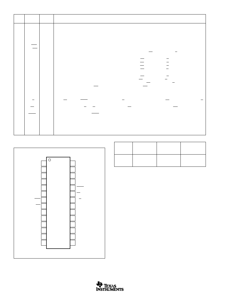
1
R1
IN
Analog Input. See Figure 7.
2
AGND1
Analog Sense Ground.
3
R2
IN
Analog Input. See Figure 7.
4
CAP
Reference Buffer Output. 2.2
µ
F tantalum capacitor to ground.
5
REF
Reference Input/Output. 2.2
µ
F tantalum capacitor to ground.
6
AGND2
Analog Ground
7
SB/BTC
I
Selects Straight Binary or Binary Two's Complement for Output Data Format.
8
EXT/INT
I
External/Internal data clock select.
9
D7
O
Data Bit 7 if BYTE is HIGH. Data bit 15 (MSB) if BYTE is LOW. Hi-Z when CS is HIGH and/or R/C is LOW. Leave
unconnected when using serial output.
10
D6
O
Data Bit 6 if BYTE is HIGH. Data bit 14 if BYTE is LOW. Hi-Z when CS is HIGH and/or R/C is LOW.
11
D5
O
Data Bit 5 if BYTE is HIGH. Data bit 13 if BYTE is LOW. Hi-Z when CS is HIGH and/or R/C is LOW.
12
D4
O
Data Bit 4 if BYTE is HIGH. Data bit 12 if BYTE is LOW. Hi-Z when CS is HIGH and/or R/C is LOW.
13
D3
O
Data Bit 3 if BYTE is HIGH. Data bit 11 if BYTE is LOW. Hi-Z when CS is HIGH and/or R/C is LOW.
14
DGND
Digital Ground
15
D2
O
Data Bit 2 if BYTE is HIGH. Data bit 10 if BYTE is LOW. Hi-Z when CS is HIGH and/or R/C is LOW.
16
D1
O
Data Bit 1 if BYTE is HIGH. Data bit 9 if BYTE is LOW. Hi-Z when CS is HIGH and/or R/C is LOW.
17
D0
O
Data Bit 0 (LSB) if BYTE is HIGH. Data bit 8 if BYTE is LOW. Hi-Z when CS is HIGH and/or R/C is LOW.
18
DATACLK
I/O
Data Clock Output when EXT/INT is LOW. Data clock input when EXT/INT is HIGH.
19
SDATA
O
Serial Output Synchronized to DATACLK
20
TAG
I
Serial Input When Using an External Data Clock
21
BYTE
I
Selects 8 most significant bits (LOW) or 8 least significant bits (HIGH) on parallel output pins.
22
R/C
I
With CS LOW and BUSY HIGH, a Falling Edge on R/C Initiates a New Conversion. With CS LOW, a rising edge on R/C
enables the parallel output.
23
CS
I
Internally OR'd with R/C. If R/C is LOW, a falling edge on CS initiates a new conversion. If EXT/INT is LOW, this same
falling edge will start the transmission of serial data results from the previous conversion.
24
BUSY
O
At the start of a conversion, BUSY goes LOW and stays LOW until the conversion is completed and the digital outputs
have been updated.
25
PWRD
I
PWRD HIGH shuts down all analog circuitry except the reference. Digital circuitry remains active.
26
REFD
I
REFD HIGH shuts down the internal reference. External reference will be required for conversions.
27
V
ANA
Analog Supply. Nominally +5V. Decouple with 0.1
µ
F ceramic and 10
µ
F tantalum capacitors.
28
V
DIG
Digital Supply. Nominally +5V. Connect directly to pin 27. Must be
V
ANA
.
DIGITAL
PIN #
NAME
I/O
DESCRIPTION
ANALOG
CONNECT R1
IN
CONNECT R2
IN
INPUT
VIA 200
VIA 100
RANGE
TO
TO
IMPEDANCE
±
10V
V
IN
CAP
45.7k
0V to 5V
AGND
V
IN
20.0k
0V to 4V
V
IN
V
IN
21.4k
TABLE I. Input Range Connections. See Figure 7.
PIN CONFIGURATION
PIN DESCRIPTIONS
Top View
DIP, SO
V
DIG
V
ANA
REFD
PWRD
BUSY
CS
R/C
BYTE
TAG
SDATA
DATACLK
D0
D1
D2
R1
IN
AGND1
R2
IN
CAP
REF
AGND2
SB/BTC
EXT/INT
D7
D6
D5
D4
D3
DGND
1
2
3
4
5
6
7
8
9
10
11
12
13
14
28
27
26
25
24
23
22
21
20
19
18
17
16
15
ADS7807

ADS7807
5
SBAS022B
www.ti.com
TYPICAL CHARACTERISTICS
At T
A
= +25
∞
C, f
S
= 40kHz, V
DIG
= V
ANA
= +5V, and using internal reference and fixed resistors (see Figure 7b), unless otherwise specified.
FREQUENCY SPECTRUM
(8192 Point FFT; f
IN
= 1kHz, 0dB)
0
≠10
≠20
≠30
≠40
≠50
≠60
≠70
≠80
≠90
≠100
≠110
≠120
≠130
0
5
10
15
20
Amplitude (dB)
Frequency (kHz)
FREQUENCY SPECTRUM
(8192 Point FFT; f
IN
= 15kHz, 0dB)
0
≠10
≠20
≠30
≠40
≠50
≠60
≠70
≠80
≠90
≠100
≠110
≠120
≠130
0
5
10
15
20
Amplitude (dB)
Frequency (kHz)
SIGNAL-TO-(NOISE + DISTORTION)
vs INPUT FREQUENCY (f
IN
= 0dB)
Input Signal Frequency (Hz)
100
1k
10k
100k
1M
100
80
90
70
60
50
40
30
20
10
SINAD (dB)
SIGNAL-TO-(NOISE + DISTORTION)
vs INPUT FREQUENCY AND INPUT AMPLITUDE
Input Signal Frequency (kHz)
0
2
4
6
8
10
12
14
16
18
20
100
80
90
70
60
50
40
30
20
10
SINAD (dB)
0dB
≠20dB
≠60dB
SIGNAL-TO-(NOISE + DISTORTION) vs TEMPERATURE
(f
IN
= 1kHz, 0dB; f
S
= 10kHz to 40kHz)
Temperature (
∞
C)
≠75
≠50
≠25
0
25
50
75
100
125
150
40kHz
100
95
90
85
80
75
SINAD (dB)
30kHz
20kHz
10kHz
AC PARAMETERS vs TEMPERATURE
(f
IN
= 1kHz, 0dB)
SFDR
THD
Temperature (
∞
C)
≠75
≠50
≠25
0
25
50
75
100
125
150
110
105
100
95
90
85
80
≠80
≠85
≠90
≠95
≠100
≠105
≠110
SFDR, SINAD, and SNR (dB)
THD (dB)
SNR
SINAD