 | –≠–ª–µ–∫—Ç—Ä–æ–Ω–Ω—ã–π –∫–æ–º–ø–æ–Ω–µ–Ω—Ç: ADS7833 | –°–∫–∞—á–∞—Ç—å:  PDF PDF  ZIP ZIP |

Æ
ADS7833
1
International Airport Industrial Park ∑ Mailing Address: PO Box 11400, Tucson, AZ 85734 ∑ Street Address: 6730 S. Tucson Blvd., Tucson, AZ 85706 ∑ Tel: (520) 746-1111 ∑ Twx: 910-952-1111
Internet: http://www.burr-brown.com/ ∑ FAXLine: (800) 548-6133 (US/Canada Only) ∑ Cable: BBRCORP ∑ Telex: 066-6491 ∑ FAX: (520) 889-1510 ∑ Immediate Product Info: (800) 548-6132
ADS7833
10-Channel, 12-Bit
DATA ACQUISITION SYSTEM
FEATURES
q
3 SIMULTANEOUS SAMPLED CHANNELS
q
3 SYNCHRONIZED 12-BIT ADCs
q
6.6
µ
s THROUGHPUT RATE
q
FULLY DIFFERENTIAL MUX INPUTS
q
DIGITALLY SELECTABLE INPUT RANGES
q
±
5V POWER SUPPLIES
q
SERIAL DIGITAL INPUT/OUTPUTS
q
2 SIMULTANEOUS SAMPLED AUXILIARY
CHANNELS
q
DIRECT INTERFACE TO MOTOROLA'S
DSP56004/7
APPLICATIONS
q
AC MOTOR SPEED CONTROLS
q
THREE PHASE POWER CONTROL
q
UNINTERRUPTABLE POWER SUPPLIES
q
VIBRATION ANALYSIS
q
PC DATA ACQUISITION
q
MEDICAL INSTRUMENTATION
Æ
ADC
2
12-Bit
PGA
2
SH
2
MUX
2
Serial Out
2
V
2-2
2
2
2
V
2-1
V
2-3
ADC
3
12-Bit
PGA
3
SH
3
MUX
3
Serial Out
3
V
3-2
2
2
2
V
3-1
V
3-4
ADC
1
12-Bit
PGA
1
SH
1
MUX
1
Serial Out
1
V
1-2
2
2
2
V
1-1
V
1-3
V
3-3
2
Control
Logic
2.5V
Ref
Input Setup
Register
DAC
8-Bit
Voltage Out
Busy
Serial IN
Convert
Clock
CAP
DAC
Input Select
Gain Select
DESCRIPTION
The ADS7833 consists of three 12-bit analog-to-digi-
tal converters preceded by three simultaneously oper-
ating sample-hold amplifiers, and multiplexers for 10
differential inputs. The ADCs have simultaneous se-
rial outputs for high speed data transfer and data
processing.
The ADS7833 also offers a programmable gain ampli-
fier with programmable gains of 1.0V/V, 1.25V/V,
2.5V/V, and 5.0V/V. Channel selection and gain se-
lection are selectable through the serial input control
word. The high through put rate is maintained by
simultaneously clocking in the 13-bit input control
word for the next conversion while the present conver-
sions are clocked out.
The part also contains an 8-bit digital-to-analog con-
verter whose digital input is supplied as part of the
input control word.
©
1994 Burr-Brown Corporation
PDS-1235C
Printed in U.S.A. May, 1997
Æ
ADS7833
2
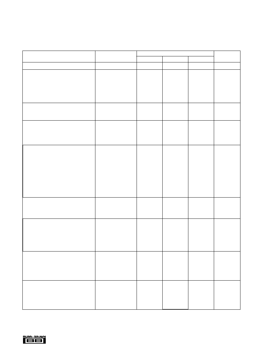
RESOLUTION
12
Bit
ANALOG INPUT
Full Scale Voltage, Differential
G = 1.0V/V
±
2.5
V
G = 1.25V/V
±
2.0
V
G = 2.5V/V
±
1.0
V
G = 5.0V/V
±
0.5
V
Common-Mode Voltage
±
0.5
See Table VII
V
Impedance
10
12
Capacitance
20
pF
THROUGHPUT SPEED
Conversion Time
CLK = 2.1MHz
6.1
µ
s
Complete Cycle
Acquire and Convert
6.6
µ
s
Throughput Rate
150
200
kHz
SAMPLING DYNAMICS
S/H Droop Rate
0.1
µ
V/
µ
s
S/H Acquisition Time
0.5
µ
s
S/H Aperture Delay
50
ns
S/H Aperture Jitter
50
ps
Sampling Skew, Channel-to-Channel
3
ns
DC ACCURACY
Integral Linearity - ADC
±
0.5
±
2
LSB
Differential Linearity - ADC
±
0.5
LSB
No Missing Codes
12
Bits
Integral Linearity - Asynchronous, Synchronous
0.5
±
3
LSB
Differential Linearity - Asynchronous, Synchronous
0.5
±
3
LSB
Full Scale Error
G = 1.0V/V
2
% of FSR
Full Scale Error Other Gains
4
% of FSR
Full Scale Error Drift
G = 1.0V/V
±
10
±
100
ppm/
∞
C
G = 2.5V/V
±
10
±
100
ppm/
∞
C
Zero Error - ADC
G = 1.0V/V
±
0.5
±
15
LSB
Zero Error - Asynchronous, Synchronous
G = 1.0V/V
±
0.5
±
20
LSB
Zero Error Drift
G = 1.0V/V
±
0.5
ppm/
∞
C
AC ACCURACY
Total Harmonic Distortion
f
IN
= 1kHz
92
dB
f
IN
= 1MHz
72
dB
CMR
V
CM
= 1V, f
CM
= 1MHz
40
dB
REFERENCE
Internal Reference Voltage
2.5
V
Internal Reference Accuracy
±
0.25
%
Internal Reference Drift
±
10
ppm/
∞
C
Internal Reference Source Current
10
µ
A
External Reference Voltage Range
2.25
2.5
2.75
V
for Specified Linearity
External Reference Current Drain
10
µ
A
DIGITAL INPUTS
Logic Levels
V
IL
0
1.5
V
V
IH
+3.5
+5
V
I
IL
±
10
µ
A
I
IH
±
10
µ
A
Input Capacitance
At All Digital Input Pins
15
pF
DIGITAL OUTPUTS
Data Format
12-Bit Serial
Data Coding
BTC
V
OL
I
SINK
= 1.6mA
0
0.4
V
V
OH
I
SOURCE
= 500
µ
A
4.2
5
V
Leakage Current
±
5
µ
A
Output Capacitance
At All Digital Output Pins
15
pF
SPECIFICATIONS
At V
ANA+
= +5V, V
ANA≠
= ≠5V, V
DIG+
= +5V, V
DIG≠
= ≠5V, and T
A
= ≠40
∞
C to +85
∞
C, using internal reference, f
CLOCK
= 2.1MHz.
ANALOG-TO-DIGITAL CONVERTER CHANNELS
ADS7833N
PARAMETER
CONDITIONS
MIN
TYP
MAX
UNITS
The information provided herein is believed to be reliable; however, BURR-BROWN assumes no responsibility for inaccuracies or omissions. BURR-BROWN assumes
no responsibility for the use of this information, and all use of such information shall be entirely at the user's own risk. Prices and specifications are subject to change
without notice. No patent rights or licenses to any of the circuits described herein are implied or granted to any third party. BURR-BROWN does not authorize or warrant
any BURR-BROWN product for use in life support devices and/or systems.

Æ
ADS7833
3
SPECIFICATIONS
(CONT)
At V
ANA+
= +5V, V
ANA≠
= ≠5V, V
DIG+
= +5V, V
DIG≠
= ≠5V, and T
A
= ≠40
∞
C to +85
∞
C, using internal reference, f
CLOCK
= 2.1MHz.
ANALOG-TO-DIGITAL CONVERTER CHANNELS
POWER SUPPLIES
Specified Performance
V
ANA+
+4.75
+5.0
+5.25
V
V
ANA≠
≠4.75
≠5.0
≠5.25
V
V
DIG+
+4.75
+5.0
+5.25
V
V
DIG≠
≠4.75
≠5.0
≠5.25
V
I
ANA+
15
25
mA
I
ANA≠
8
10
mA
I
DIG+
3
5
mA
I
DIG≠
1
2
mA
Power Dissipation
125
mW
TEMPERATURE RANGE
Specified Performance
≠40
+85
∞
C
Derated Performance
≠55
+125
∞
C
Storage
≠65
+150
∞
C
ADS7833N
PARAMETER
CONDITIONS
MIN
TYP
MAX
UNITS
RESOLUTION
8-Bits
Output Range
0
+2.5
V
Output Settling Time
To 0.5LSB
1
µ
s
Linearity Error
±
1
LSB
Differential Linearity
±
1
LSB
Output Current
200
µ
A
Offset Error
±
1
10
mV
Full Scale Error
2
%
DIGITAL-TO-ANALOG CONVERTER
ADS7833N
PARAMETER
CONDITIONS
MIN
TYP
MAX
UNITS
ABSOLUTE MAXIMUM RATINGS
Analog Input Voltage ............................................... ..........................
±
25V
Ground Voltage Difference: AGND and DGND .................................
±
0.3V
Power Supply Voltages:
V
ANA+
................................................................................................. +7V
V
ANA≠
................................................................................................. ≠7V
V
DIG+
................................................................................................. +7V
V
DIG≠
................................................................................................. ≠7V
Digital Inputs .............................................................. ≠0.3V to V
DIG
+0.3V
Maximum Junction Temperature ................................................... +165
∞
C
Internal Power Dissipation ............................................................. 825mW
Lead Temperature (soldering, 10s) ............................................... +300
∞
C
PIN CONFIGURATION
SYMBOL
DESCRIPTION
MIN TYP MAX UNITS
t
CONV
A/D Conversion Time
6.6
4.0
µ
s
CLK
A/D Conversion Clock
2.1
2.8
MHz
t
1
Setup Time for Conversion
50
ns
Before Rising Edge of Clock
t
2
Hold Time for Conversion
50
ns
After Rising Edge of Clock
t
3
Setup Time for Serial Out
25
ns
t
4
Setup Time for Serial Input
30
ns
t
5
Hold Time for Serial Input
30
ns
CONVERSION AND DATA TIMING
PACKAGE INFORMATION
PACKAGE DRAWING
PRODUCT
PACKAGE
NUMBER
(1)
ADS7833N
68-Lead PLCC
312
NOTE: (1) For detailed drawing and dimension table, please see end of data
sheet, or Appendix C of Burr-Brown IC Data Book.
4
3
2
1
ADS7833N
68 67 66
NC
V
2-1N
V
2-1P
NC
V
2-2N
V
2-2P
NC
V
2-3N
V
2-3P
NC
NC
NC
NC
NC
NC
NC
NC
NC
V
1-1N
V
1-1P
NC
V
1-2N
V
1-2P
NC
V
1-3N
V
1-3P
NC
NC
NC
NC
NC
NC
NC
NC
V
3-1P
V
3-1N
NC
V
3-2P
V
3-2N
V
3-3P
V
3-3N
V
3-4P
V
3-4N
V
ANA+
AGND
V
ANA≠
REF
GND
REF
IN
CAP
A
OUT
NC
10
11
12
13
14
15
16
17
18
19
20
21
22
23
24
25
26
65 64 63 62 61
60
59
58
57
56
55
54
53
52
51
50
49
48
47
46
45
44
9
8
7
6
5
32 33 34 35 36 37 38
TP
1
TP
2
V
DIG+
DGND
V
DIG≠
NC
S
OUT2
S
OUT3
S
OUT1
CLK
CONV
ASH
SER
IN
BUSY
DCLOCK
NC
NC
39 40 41 42 43
27 28 29 30 31

Æ
ADS7833
4
PIN DEFINITIONS
PIN NO
NAME
TYPE
(1)
DESCRIPTION
1
V
3≠4N
AI
Voltage Input, Channel 3, Mux I/P 4,
Negative Side
2
V
3≠4P
AI
Voltage Input, Channel 3, Mux IP 4,
Positive Side
3
V
3≠3N
AI
Voltage Input, Channel 3, Mux I/P 3,
Negative Side
4
V
3≠3P
AI
Voltage Input, Channel 3, Mux I/P 3,
Positive Side
5
V
3≠2N
AI
Voltage Input, Channel 3, Mux I/P 2,
Negative Side
6
V
3≠2P
AI
Voltage Input, Channel 3, Mux I/P 2,
Positive Side
7
NC
--
No Connection
8
V
3≠1N
AI
Voltage Input, Channel 3, Mux I/P 1,
Negative Side
9
V
3≠1P
AI
Voltage Input, Channel 3, Mux I/P 1,
Positive Side
10
NC
--
No Connection
11
V
2≠1N
AI
Voltage Input, Channel 2, Mux I/P 1,
Negative Side
12
V
2≠1P
AI
Voltage Input, Channel 2, Mux I/P 1,
Positive Side
13
NC
--
No Connection
14
V
2≠2N
AI
Voltage Input, Channel 2, Mux I/P 2,
Negative Side
15
V
2≠2P
AI
Voltage Input, Channel 2, Mux I/P 2,
Positive Side
16
NC
--
No Connection
17
V
2≠3N
AI
Voltage Input, Channel 2, Mux I/P 3,
Negative Side.
18
V
2≠3P
AI
Voltage Input, Channel 2, Mux I/P 3,
Positive Side
19
NC
--
No Connection
20
NC
--
No Connection
21
NC
--
No Connection
22
NC
--
No Connection
23
NC
--
No Connection
24
NC
--
No Connection
25
NC
--
No Connection
26
NC
--
No Connection
27
TP1
--
Test Point 1, Make No Connection
28
TP2
--
Test Point 2, Make No Connection
29
V
DIG+
P
Digital Supply Voltage, +5V
30
DGND
P
Digital Supply Voltage, Ground
31
V
DIG≠
P
Digital Supply Voltage, ≠5V
32
NC
--
No Connection
33
S
OUT2
DO
Serial Digital Output, Channel 2
34
S
OUT3
DO
Serial Digital Output, Channel 3
35
S
OUT1
DO
Serial Digital Output, Channel 1
36
CLK
DI
Clock for A/D Converters
37
CONV
DI
Start A/D Converters. When CONV goes to
"0" (low) the next rising edge of CLK
starts the conversion.
38
ASH
DI
Digital Control for Asynchronous Sample
Hold. If signal is "1" (high), signals
are sampled.
39
SER
IN
DI
Serial Digital Input for Input Control Word
40
BUSY
DO
A/D Converters Busy. Busy if signal
is "0" (low).
41
DCLOCK
DO
A Delayed and Truncated Version of
the CLK Signals. It is Delayed 50ns
from the CLK Signal and Stays Low
after 13 DCLOCK Cycles.
42
NC
--
No Connection
43
NC
--
No Connection
44
NC
--
No Connection
45
NC
--
No Connection
46
NC
--
No Connection
47
NC
--
No Connection
48
NC
--
No Connection
49
NC
--
No Connection
50
NC
--
No Connection
51
NC
--
No Connection
52
V
1≠3P
AI
Voltage Input, Channel 1, Mux I/P 3,
Positive Side
53
V
1≠3N
AI
Voltage Input, Channel 1, Mux I/P 3,
Negative Side
54
NC
--
No Connection
55
V
1≠2P
AI
Voltage Input, Channel 1, Mux I/P 2,
Positive Side
56
V
1≠2N
AI
Voltage Input, Channel 1, Mux I/P 2,
Negative Side
57
NC
--
No Connection
58
V
1≠1P
AI
Voltage Input, Channel 1, Mux I/P 1,
Positive Side
59
V
1≠1N
AI
Voltage Input, Channel 1, Mux I/P 1,
Negative Side
60
NC
--
No Connection
61
NC
--
No Connection
62
A
OUT
AO
Output of DAC
63
CAP
AO
Decoupling Point for Internal Reference
64
REF
IN
AI
Input Pin for External Reference
65
REF
GND
P
Ground Pin for External Reference
66
V
ANA≠
P
Analog Supply Voltage, ≠5V
67
AGND
P
Analog Supply Voltage, Ground
68
V
ANA+
P
Analog Supply Voltage, +5V
PIN NO
NAME
TYPE
(1)
DESCRIPTION
NOTE: (1) AI is Analog Input, AO is Analog Output, DI is Digital Input, DO is Digital Output, P is Power Supply Connection.

Æ
ADS7833
5
TYPICAL PERFORMANCE CURVES
At V
ANA+
= +5V, V
ANA≠
= ≠5V, V
DIG+
= +5V, V
DIG≠
= ≠5V and T
A
= 25
∞
C, using internal reference, f
CLOCK
= 2.1MHz.
OFFSET vs TEMPERATURE
Temperature (∞C)
1.4
1.2
1.0
0.8
0.6
0.4
0.2
0
≠55
≠40
≠25
0
25
70
85
125
Offset (LSB)
FULL SCALE vs TEMPERATURE
Temperature (∞C)
0.9
0.8
0.7
0.6
0.5
0.4
0.3
0.2
0.1
0
≠55
≠40
≠25
0
25
70
85
125
Full Scale (%)
DIFFERENTIAL LINEARITY (MIN) vs TEMPERATURE
Temperature (∞C)
0.000
≠0.100
≠0.200
≠0.300
≠0.400
≠0.500
≠0.600
≠0.700
≠55
≠40
≠25
0
25
70
85
125
Differential Linearity (LSB)
DIFFERENTIAL LINEARITY (MAX) vs TEMPERATURE
Temperature (∞C)
0.40
0.35
0.30
0.25
0.20
0.15
0.10
0.05
0
≠55
≠40
≠25
0
25
70
85
125
Differential Linearity (LSB)
INTEGRAL LINEARITY (MIN) vs TEMPERATURE
Temperature (∞C)
0.000
≠0.050
≠0.100
≠0.150
≠0.200
≠0.250
≠0.300
≠0.350
≠0.400
≠0.450
≠55
≠40
≠25
0
25
70
85
125
Integral Linearity (LSB)
INTEGRAL LINEARITY (MAX) vs TEMPERATURE
Temperature (∞C)
0.45
0.40
0.35
0.30
0.25
0.20
0.15
0.10
0.05
0
≠55
≠40
≠25
0
25
70
85
125
Integral Linearity (LSB)