 | –≠–ª–µ–∫—Ç—Ä–æ–Ω–Ω—ã–π –∫–æ–º–ø–æ–Ω–µ–Ω—Ç: ADS807E | –°–∫–∞—á–∞—Ç—å:  PDF PDF  ZIP ZIP |

ADS807
Æ
12-Bit, 53MHz Sampling
ANALOG-TO-DIGITAL CONVERTER
FEATURES
q
SPURIOUS FREE DYNAMIC RANGE:
82dB at 10MHz f
IN
q
HIGH SNR: 67.5dB (2Vp-p), 69dB (3Vp-p)
q
LOW POWER: 335mW
q
INTERNAL OR EXTERNAL REFERENCE
q
LOW DNL: 0.5LSB
q
FLEXIBLE INPUT RANGE: 2Vp-p to 3Vp-p
q
28-LEAD SSOP PACKAGE
TM
DESCRIPTION
The ADS807 is a high-speed, high dynamic range,
12-bit pipelined analog-to-digital converter. This con-
verter includes a high-bandwidth track-and-hold that
gives excellent spurious performance up to and beyond
the Nyquist rate. The differential nature of this track-
and-hold and A/D circuitry minimizes even-order har-
monics and gives excellent common-mode noise immu-
nity. The track-and-hold can also be operated single-
ended.
The ADS807 provides for setting the full-scale range
of the converter without any external reference cir-
cuitry. The internal reference can be disabled allowing
low drive, internal references to be used for improved
tracking in multichannel systems.
The ADS807 provides an overrange indicator flag to
indicate an input signal that exceeds the full-scale input
range of the converter. This flag can be used to reduce
the gain of front end gain control circuitry. There is
also an output enable pin to allow for multiplexing and
testability on a PC board.
The ADS807 employs digital error correction tech-
niques to provide excellent differential linearity for
demanding imaging applications.
APPLICATIONS
q
COMMUNICATIONS IF PROCESSING
q
COMMUNICATIONS BASESTATIONS
q
TEST EQUIPMENT
q
MEDICAL IMAGING
q
VIDEO DIGITIZING
q
CCD DIGITIZING
©
1998 Burr-Brown Corporation
PDS-1396C
Printed in U.S.A. January, 1999
ADS807E
Pipelined
A/D
Internal
Reference
Optional External
Reference
Timing
Circuitry
Error
Correction
Logic
3-State
Outputs
T/H
D0
∑
∑
∑
D11
CLK
ADS807
OE
IN
INT/EXT
IN
CM
+2.5V
+2.5V
+3V
+2V
+2V
+3V
FS
SEL
(Opt.)
International Airport Industrial Park ∑ Mailing Address: PO Box 11400, Tucson, AZ 85734 ∑ Street Address: 6730 S. Tucson Blvd., Tucson, AZ 85706 ∑ Tel: (520) 746-1111
Twx: 910-952-1111 ∑ Internet: http://www.burr-brown.com/ ∑ Cable: BBRCORP ∑ Telex: 066-6491 ∑ FAX: (520) 889-1510 ∑ Immediate Product Info: (800) 548-6132

2
Æ
ADS807
ADS807E
PARAMETER
CONDITIONS
MIN
TYP
MAX
UNITS
RESOLUTION
12 Guaranteed
Bits
Specified Temperature Range
Ambient Air
≠40
+85
∞
C
ANALOG INPUT
2V Full-Scale Input Range (Differential)
2Vp-p, INT or EXT Ref
2
3
V
2V Full-Scale Input Range (Single-Ended)
2Vp-p, INT or EXT Ref
1.5
3.5
V
3V Full-Scale Input Range (Differential)
3Vp-p, INT or EXT Ref
1.75
3.25
V
3V Full-Scale Input Range (Single-Ended)
3Vp-p, INT or EXT Ref
1
4
V
Analog Input Bias Current
1
µ
A
Analog Input Bandwidth
270
MHz
Input Impedance
1.25 || 3
M
|| pF
CONVERSION CHARACTERISTICS
Sample Rate
10k
53M
Samples/s
Data Latency
6
Clock Cycles
DYNAMIC CHARACTERISTICS
Differential Linearity Error (largest code error)
f = 1MHz
±
0.5
±
1.0
LSB
f = 10MHz
f
S
= 40MHz
±
0.5
±
1.0
LSB
No Missing Codes
f
S
= 50MHz,T
A
= +25
∞
C
Guaranteed
No MIssing Codes
f
S
= 40MHz, Full Temp
Guaranteed
Integral Nonlinearity Error, f = 1MHz
±
2.0
±
4.0
LSBs
Spurious Free Dynamic Range
(1)
f = 1MHz (≠1dB input)
83
dBFS
(2)
f = 10MHz (≠1dB input)
67
82
dBFS
f = 20MHz (≠1dB input)
76
dBFS
f = 40MHz (undersampling)
76
dBFS
f = 1MHz to 10MHz, f
S
= 40MHz
2Vp-p, Single-Ended Input
62
69
dBFS
Two-Tone Intermodulation Distortion
(3)
f = 12MHz and 13MHz (≠7dB each tone)
71
dBc
Signal-to-Noise Ratio (SNR)
f = 1MHz (≠1dB input)
63
68
dB
f = 10MHz (≠1dB input)
63
68
dB
f = 20MHz (≠dB input)
66
dB
f = 40MHz (undersampling)
67
dB
f = 1MHz to 10MHz, f
S
= 40MHz
63
67.5
dB
f = 1MHz to 10MHz, f
S
= 40MHz
2Vp-p, Single-Ended Input
60
67
dB
f = 1MHz (≠1dB input)
3Vp-p
69
dB
f = 10MHz (≠1dB input)
3Vp-p
69
dB
Signal-to-(Noise + Distortion) (SINAD)
(4)
f = 1MHz (≠1dBFS input)
61
67
dB
f = 10MHz (≠1dBFS input)
61
67
dB
f = 20MHz (≠1dBFS input)
67
dB
f = 1MHz to 10MHz, f
S
= 40MHz
63
67
dB
f = 1MHz to 10MHz, f
S
= 40MHz
2Vp-p, Single-Ended Input
60
64
dB
f = 1MHz (≠1dBFS input)
3Vp-p
69
dB
f = 10MHz (≠dBFS Input)
3Vp-p
69
dB
Output Noise
Input Grounded
0.2
LSBs rms
Aperture Delay Time
2
ns
Aperture Jitter
1.2
ps rms
Overvoltage Recovery Time
2
ns
DIGITAL INPUTS
Logic Family
Convert Command
Start Conversion
High Level Input Current
(5)
(V
IN
= 5V)
+50
µ
A
Low Level Input Current (V
IN
= 0V)
+10
µ
A
High Level Input Voltage
+2.4
V
Low Level Input Voltage
+1.0
V
Input Capacitance
5
pF
SPECIFICATIONS
At T
A
= full specified temperature range, V
S
= +5V, differential input range = 2V to 3V for each input, sampling rate = 50MHz, unless otherwise noted.
CMOS
Rising Edge of Convert Clock

3
Æ
ADS807
SPECIFICATIONS
At T
A
= full specified temperature range, V
S
= +5V, differential input range = 2V to 3V for each input, sampling rate = 50MHz, unless otherwise noted.
ADS807E
PARAMETER
CONDITIONS
MIN
TYP
MAX
UNITS
The information provided herein is believed to be reliable; however, BURR-BROWN assumes no responsibility for inaccuracies or omissions. BURR-BROWN assumes no responsibility
for the use of this information, and all use of such information shall be entirely at the user's own risk. Prices and specifications are subject to change without notice. No patent rights
or licenses to any of the circuits described herein are implied or granted to any third party. BURR-BROWN does not authorize or warrant any BURR-BROWN product for use in life
support devices and/or systems.
CMOS
Straight Offset Binary
DIGITAL OUTPUTS
Logic Family
Logic Coding
Low Output Voltage (I
OL
= 50
µ
A)
VDRV = 5V
+0.1
V
Low Output Voltage, (I
OL
= 1.6mA)
VDRV = 5V
+0.2
V
High Output Voltage, (I
OH
= 50
µ
A)
VDRV = 5V
+4.9
V
High Output Voltage, (I
OH
= 0.5mA)
VDRV = 5V
+4.8
V
Low Output Voltage, (I
OL
= 50
µ
A)
VDRV = 3V
+0.1
V
High Output Voltage, (I
OH
= 50
µ
A)
VDRV = 3V
+2.8
V
3-State Enable Time
OE = L
(5)
20
40
ns
3-State Disable Time
OE = H
(5)
2
10
ns
Output Capacitance
5
pF
ACCURACY (Internal Reference, 2Vp-p, Unless Otherwise Noted)
Zero Error (Referred to ≠FS)
at 25
∞
C
±
1.0
±
2.0
%FS
Zero Error Drift (Referred to ≠FS)
16
ppm/
∞
C
Gain Error
(6)
at 25
∞
C
±
1.5
±
2.5
%FS
Gain Error Drift
(6)
66
ppm/
∞
C
Gain Error
(7)
at 25
∞
C
±
1.0
±
1.5
%FS
Gain Error Drift
(7)
23
ppm/
∞
C
Power Supply Rejection of Gain
V
S
=
±
5%
50
70
dB
REFT Tolerance
2V Full Scale
Deviation From Ideal 3.0V
±
10
±
65
mV
3V Full Scale
Deviation From Ideal 3.25V
±
20
±
100
mV
REFB Tolerance
2V Full Scale
Deviation From Ideal 2.0V
±
10
±
65
mV
3V Full Scale
Deviation From Ideal 1.75V
±
20
±
100
mV
External REFT Voltage Range
REFB + 0.4
3
V
S
≠ 1.70
V
External REFB Voltage Range
1.70
2
REFT ≠ 0.4
V
Reference Input Resistance
1
k
POWER SUPPLY REQUIREMENTS
Supply Voltage: +V
S
Operating
+4.75
+5.0
+5.25
V
Supply Current: +I
S
Operating
60
mA
Power Dissipation: VDRV = 5V
External Reference
305
360
mW
VDRV = 3V
External Reference
290
350
mW
VDRV = 5V
Internal Reference
350
390
mW
VDRV = 3V
Internal Reference
335
380
mW
Thermal Resistance,
JA
28-Lead SSOP
50
∞
C/W
NOTES: (1) Spurious Free Dynamic Range refers to the magnitude of the largest harmonic. (2) dBFS means dB relative to Full Scale. (3) Two-tone intermodulation
distortion is referred to the largest fundamental tone. This number will be 6dB higher if it is referred to the magnitude of the two-tone fundamental envelope.
(4) Effective number of bits (ENOB) is defined by as (SINAD ≠ 1.76) /6.02. (5) A 50k
pull-down resistor is inserted internally on OE pin. (6) Includes internal reference.
(7) Excludes internal reference.

4
Æ
ADS807
PIN DESCRIPTIONS
+V
S
....................................................................................................... +6V
Analog Input ........................................................... (≠0.3V) to (+V
S
+ 0.3V)
Logic Input ............................................................. (≠0.3V) to (+V
S
+ 0.3V)
Case Temperature ......................................................................... +100
∞
C
Junction Temperature .................................................................... +150
∞
C
Storage Temperature ..................................................................... +150
∞
C
ABSOLUTE MAXIMUM RATINGS
Top View
SSOP
PIN CONFIGURATION
PIN
DESIGNATOR
DESCRIPTION
1
GND
Ground
2
Bit 1
Data Bit 1 (MSB)
3
Bit 2
Data Bit 2
4
Bit 3
Data Bit 3
5
Bit 4
Data Bit 4
6
Bit 5
Data Bit 5
7
Bit 6
Data Bit 6
8
Bit 7
Data Bit 7
9
Bit 8
Data Bit 8
10
Bit 9
Data Bit 9
11
Bit 10
Data Bit 10
12
Bit 11
Data Bit 11
13
Bit 12
Data Bit 12 (LSB)
14
CLK
Convert Clock
15
+V
S
+5V Supply
16
FS
SEL
HI = 3V, LO = 2V
17
OTR
Out of Range Indicator
18
INT/EXT
Reference Select: HIGH or Floating = Exter-
nal LOW = Internal 50k
pull up
19
OE
Output Enable
20
GND
Ground
21
REFB
Bottom Reference/Bypass
22
REFT
Top Reference/Bypass
23
CM
Common-Mode Voltage Output
24
IN
Complementary Analog Input
25
IN
Analog Input
26
GND
Ground
27
+V
S
+5V Supply
28
VDRV
Logic Driver Supply Voltage
ELECTROSTATIC
DISCHARGE SENSITIVITY
This integrated circuit can be damaged by ESD. Burr-Brown
recommends that all integrated circuits be handled with
appropriate precautions. Failure to observe proper handling and
installation procedures can cause damage.
ESD damage can range from subtle performance degradation to
complete device failure. Precision integrated circuits may be
more susceptible to damage because very small parametric
changes could cause the device not to meet its published
specifications.
GND
Bit 1 (MSB)
Bit 2
Bit 3
Bit 4
Bit 5
Bit 6
Bit 7
Bit 8
Bit 9
Bit 10
Bit 11
Bit 12 (LSB)
CLK
VDRV
+V
S
GND
IN
IN
CM
REFT
REFB
GND
OE
INT/EXT
OTR
FS
SEL
+V
S
1
2
3
4
5
6
7
8
9
10
11
12
13
14
28
27
26
25
24
23
22
21
20
19
18
17
16
15
ADS807E
PACKAGE
SPECIFIED
DRAWING
TEMPERATURE
PACKAGE
ORDERING
TRANSPORT
PRODUCT
PACKAGE
NUMBER
(1)
RANGE
MARKING
NUMBER
(2)
MEDIA
ADS807E
28-Lead SSOP
324
≠40
∞
C to +85
∞
C
ADS807E
ADS807E
Tube
"
"
"
"
"
ADS807E/1K
Tape and Reel
NOTES: (1) For detailed drawing and dimension table, please see end of data sheet, or Appendix C of Burr-Brown IC Data Book or download from www.burr-
brown.com. (2) Models with a slash (/) are available only in Tape and Reel in the quantities indicated (e.g., /1K indicates 1000 devices per reel). Ordering 1000
pieces of "ADS807E/1K" will get a single 1000-piece Tape and Reel. For detailed Tape and Reel mechanical information, refer to Appendix B of Burr-Brown IC
Data Book.
PACKAGE/ORDERING INFORMATION
5
Æ
ADS807
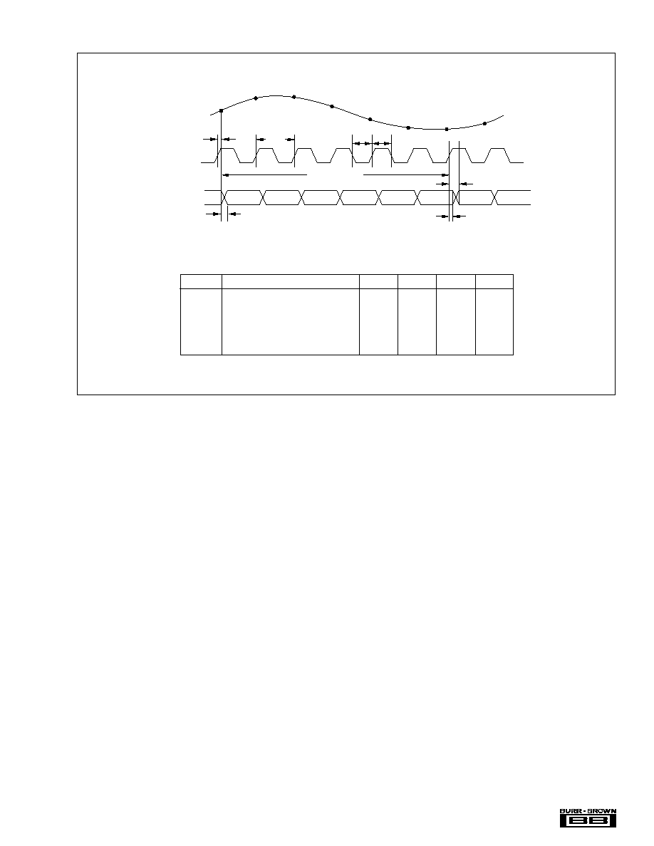
TIMING DIAGRAM
6 Clock Cycles
Data Invalid
t
D
t
L
t
H
t
CONV
N≠6
N≠5
N≠4
N≠3
N≠2
N≠1
N
N+1
Data Out
Clock
Analog In
N
t
2
N+1
N+2
N+3
N+4
N+5
N+6
N+7
t
1
SYMBOL
DESCRIPTION
MIN
TYP
MAX
UNITS
t
CONV
Convert Clock Period
18.87
100
µ
s
ns
t
L
Clock Pulse Low
9.4
t
CONV
/2
ns
t
H
Clock Pulse High
9.4
t
CONV
/2
ns
t
D
Aperture Delay
2
ns
t
1
(1)
Data Hold Time, C
L
= 0pF
2.7
ns
t
2
(1)
New Data Delay Time, C
L
= 15pF max
12
ns
NOTE: (1) t
1
and t
2
times are valid for VDRV voltages of +2.7V to +5V.