
10-Bit, 40MHz Sampling
ANALOG-TO-DIGITAL CONVERTER
FEATURES
q
NO MISSING CODES
q
INTERNAL REFERENCE
q
LOW POWER: 380mW
q
HIGH SNR: 58dB
q
INTERNAL TRACK-AND-HOLD
DESCRIPTION
The ADS821 is a low-power, monolithic 10-bit, 40MHz Ana-
log-to-Digital (A/D) converter utilizing a small geometry CMOS
process. This complete converter includes a 10-bit quantizer
with internal track-and-hold, reference, and a power-down
feature. It operates from a single +5V power supply and can
be configured to accept either differential or single-ended
input signals.
The ADS821 employs digital error correction to provide
excellent Nyquist differential linearity performance for de-
manding imaging applications. Its low distortion, high SNR,
and high oversampling capability give it the extra margin
needed for telecommunications and video applications.
This high-performance converter is specified for AC and DC-
performance at a 40MHz sampling rate. The ADS821 is
available in an SO-28 package.
APPLICATIONS
q
VIDEO DIGITIZING
q
ULTRASOUND IMAGING
q
GAMMA CAMERAS
q
SET-TOP BOXES
q
CABLE MODEMS
q
CCD IMAGING
Color Copiers
Scanners
Camcorders
Security Cameras
Fax Machines
q
IF AND BASEBAND DIGITIZATION
q
TEST INSTRUMENTATION
ADS821
SBAS040B � DECEMBER 1995 � REVISED FEBRUARY 2005
www.ti.com
Copyright � 1995-2005, Texas Instruments Incorporated
Please be aware that an important notice concerning availability, standard warranty, and use in critical applications of
Texas Instruments semiconductor products and disclaimers thereto appears at the end of this data sheet.
Pipeline
A/D
Converter
Timing
Circuitry
Error
Correction
Logic
3-State
Outputs
T&H
10-Bit
Digital
Data
CLK
+1.25V
+3.25V
MSBI
OE
IN
IN
REFT
CM
REFB
PRODUCTION DATA information is current as of publication date.
Products conform to specifications per the terms of Texas Instruments
standard warranty. Production processing does not necessarily include
testing of all parameters.
ADS8
21U
All trademarks are the property of their respective owners.

www.ti.com
ADS821
2
SBAS040B
RESOLUTION
10
Bits
Specified Temperature Range
T
AMBIENT
�40
+85
�
C
ANALOG INPUT
Differential Full-Scale Input Range
+1.25
+3.25
V
Common-Mode Voltage
+2.25
V
Analog Input Bandwidth (�3dB)
Small-Signal
�20dBFS
(1)
Input
+25
�
C
400
MHz
Full-Power
0dBFS Input
+25
�
C
65
MHz
Input Impedance
1.25 || 4
M
|| pF
DIGITAL INPUT
Logic Family
Convert Command
Start Conversion
ACCURACY
(2)
Gain Error
+25
�
C
�
0.6
�
1.5
%
Full
�
1.1
�
2.5
%
Gain Drift
�
85
ppm/
�
C
Power-Supply Rejection of Gain
+V
S
=
�
5%
+25
�
C
0.01
0.15
%FSR/%
Input Offset Error
Full
�
2.1
�
3.5
%
Power-Supply Rejection of Offset
+V
S
=
�
5%
+25
�
C
0.02
0.15
%FSR/%
CONVERSION CHARACTERISTICS
Sample Rate
10k
40M
Sample/s
Data Latency
6.5
Convert Cycle
DYNAMIC CHARACTERISTICS
Differential Linearity Error
t
H
= 13ns
(3)
f = 500kHz
+25
�
C
�
0.5
�
1.0
LSB
0
�
C to +70
�
C
�
0.6
�
1.0
LSB
f = 12MHz
+25
�
C
�
0.5
�
1.0
LSB
0
�
C to +70
�
C
�
0.6
�
1.0
LSB
No Missing Codes
0
�
C to +70
�
C
Tested
Integral Linearity Error at f = 500kHz
0
�
C to +70
�
C
�
0.5
�
2.0
LSB
Spurious-Free Dynamic Range (SFDR)
f = 500kHz (�1dBFS input)
+25
�
C
60
70
dBFS
Full
54
67
dBFS
f = 12MHz (�1dBFS input)
+25
�
C
58
63
dBFS
Full
54
62
dBFS
ADS821U
PARAMETER
CONDITIONS
TEMP
MIN
TYP
MAX
UNITS
ELECTRICAL CHARACTERISTICS
At T
A
= +25
�
C, V
S
= +5V, Sampling Rate = 40MHz, and with a 50% duty cycle clock having a 2ns rise-and-fall time, unless otherwise noted.
ABSOLUTE MAXIMUM RATINGS
(1)
+V
S
....................................................................................................... +6V
Analog Input ............................................................ 0V to (+V
S
+ 300mV)
Logic Input ............................................................... 0V to (+V
S
+ 300mV)
Case Temperature ......................................................................... +100
�
C
Junction Temperature .................................................................... +150
�
C
Storage Temperature .................................................................... +125
�
C
External Top Reference Voltage (REFT) ................................. +3.4V max
External Bottom Reference Voltage (REFB) ............................ +1.1V min
NOTES: (1) Stresses above these ratings may cause permanent damage.
Exposure to absolute maximum conditions for extended periods may degrade
device reliability.
ELECTROSTATIC
DISCHARGE SENSITIVITY
This integrated circuit can be damaged by ESD. Texas Instru-
ments recommends that all integrated circuits be handled with
appropriate precautions. Failure to observe proper handling
and installation procedures can cause damage.
ESD damage can range from subtle performance degradation
to complete device failure. Precision integrated circuits may be
more susceptible to damage because very small parametric
changes could cause the device not to meet its published
specifications.
SPECIFIED
PACKAGE
TEMPERATURE
PACKAGE
ORDERING
TRANSPORT
PRODUCT
PACKAGE-LEAD
DESIGNATOR
RANGE
MARKING
NUMBER
MEDIA, QUANTITY
ADS821
SO-8
DW
�40
�
C to +85
�
C
ADS821U
ADS821U
Rails, 28
"
"
"
"
"
ADS821U/1K
Tape and Reel, 1000
PACKAGE/ORDERING INFORMATION(1)
NOTE: (1) For the most current package and ordering information, see the Package Option Addendum at the end of this document, or see the TI website at
www.ti.com.
TTL/HCT Compatible CMOS
Falling Edge
NOTES: (1) dBFS refers to dB below Full-Scale. (2) Percentage accuracies are referred to the internal A/D converter Full-Scale Range of 4Vp-p. (3) Refer to Timing
Diagram footnotes for the differential linearity performance conditions for the SO and SSOP packages. (4) IMD is referred to the larger of the two input signals.
If referred to the peak envelope signal (
0dB), the intermodulation products will be 7dB lower. (5) Based on (SINAD � 1.76)/6.02. (6) No "rollover" of bits.

www.ti.com
ADS821
3
SBAS040B
DYNAMIC CHARACTERISTICS (Cont.)
2-Tone Intermodulation Distortion (IMD)
(4)
f = 4.4MHz and 4.5MHz (�7dBFS each tone)
+25
�
C
�61
dBc
Full
�60
dBc
Signal-to-Noise Ratio (SNR)
f = 500kHz (�1dBFS input)
+25
�
C
57
59
dB
Full
55
59
dB
f = 12MHz (�1dBFS input)
+25
�
C
56
58
dB
Full
54
58
dB
Signal-to-(Noise + Distortion) (SINAD)
f = 500kHz (�1dBFS input)
+25
�
C
56
58.5
dB
Full
52
58
dB
f = 12MHz (�1dBFS input)
+25
�
C
53
57
dB
Full
50
56
dB
Differential Gain Error
NTSC or PAL
+25
�
C
0.5
%
Differential Phase Error
NTSC or PAL
+25
�
C
0.1
Degrees
Effective Bits
(5)
f
IN
= 3.58MHz
+25
�
C
9.3
Bits
Aperture Delay Time
+25
�
C
2
ns
Aperture Jitter
+25
�
C
7
ps rms
Over-Voltage Recovery Time
(6)
1.5x Full-Scale Input
+25
�
C
2
ns
OUTPUTS
Logic Family
Logic Coding
Logic Selectable
Logic Levels
Logic LOW,
Full
0
0.4
V
C
L
= 15pF max
Logic HIGH,
Full
+2.5
+V
S
V
C
L
= 15pF max
3-State Enable Time
20
40
ns
3-State Disable Time
Full
2
10
ns
POWER-SUPPLY REQUIREMENTS
Supply Voltage: +V
S
Operating
Full
+4.75
+5
+5.25
V
Supply Current: +I
S
Operating
+25
�
C
76
88
mA
Operating
Full
78
90
mA
Power Consumption
Operating
+25
�
C
380
440
mW
Operating
Full
390
450
mW
Thermal Resistance,
JA
75
�
C/W
ELECTRICAL CHARACTERISTICS
(Cont.)
At T
A
= +25
�
C, V
S
= +5V, Sampling Rate = 40MHz, and with a 50% duty cycle clock having a 2ns rise-and-fall time, unless otherwise noted.
NOTES: (1) dBFS refers to dB below Full Scale. (2) Percentage accuracies are referred to the internal A/D converter Full-Scale Range of 4Vp-p. (3) Refer to Timing
Diagram footnotes for the differential linearity performance conditions for the SO and SSOP packages. (4) IMD is referred to the larger of the two input signals.
If referred to the peak envelope signal (
0dB), the intermodulation products will be 7dB lower. (5) Based on (SINAD � 1.76)/6.02. (6) No "rollover" of bits.
ADS821U
PARAMETER
CONDITIONS
TEMP
MIN
TYP
MAX
UNITS
TTL/HCT Compatible CMOS
SOB or BTC

www.ti.com
ADS821
4
SBAS040B
PIN
DESIGNATOR
DESCRIPTION
1
GND
Ground
2
B1
Bit 1, Most Significant Bit (MSB)
3
B2
Bit 2
4
B3
Bit 3
5
B4
Bit 4
6
B5
Bit 5
7
B6
Bit 6
8
B7
Bit 7
9
B8
Bit 8
10
B9
Bit 9
11
B10
Bit 10, Least Significant Bit (LSB)
12
DNC
Do Not Connect
13
DNC
Do Not Connect
14
GND
Ground
15
+V
S
+5V Power Supply
16
CLK
Convert Clock Input, 50% Duty Cycle
17
+V
S
+5V Power Supply
18
OE
HIGH: High-Impedance State. LOW or Floating:
Normal Operation. Internal pull-down resistor.
19
MSBI
Most Significant Bit Inversion, HIGH: MSB in-
verted for complementary output. LOW or Float-
ing: Straight output. Internal pull-down resistor.
20
+V
S
+5V Power Supply
21
REFB
Bottom Reference Bypass. For external bypass-
ing of internal +1.25V reference.
22
CM
Common-Mode Voltage. It is derived by (REFT +
REFB)/2.
23
REFT
Top Reference Bypass. For external bypassing
of internal +3.25V reference.
24
+V
S
+5V Power Supply
25
GND
Ground
26
IN
Input
27
IN
Complementary Input
28
GND
Ground
PIN DESCRIPTIONS
PIN CONFIGURATION
Top View
SO
TIMING DIAGRAM
SYMBOL
DESCRIPTION
MIN
TYP
MAX
UNITS
t
CONV
Convert Clock Period
25
100
�
s
ns
t
L
Clock Pulse LOW
12
12.5
ns
t
H
Clock Pulse HIGH
12
(2)
12.5
ns
t
D
Aperture Delay
2
ns
t
1
Data Hold Time, C
L
= 0pF
3.9
ns
t
2
New Data Delay Time, C
L
= 15pF max
12.5
ns
NOTES: (1) " " indicates the portion of the waveform that will stretch out at slower sample rates.
(2) t
H
must be 13ns minimum if no missing codes is desired only for the conditions of t
CONV
28ns
and f
IN
< 2MHz for the SO package. For best performance in the SSOP package, t
H
must be 13ns
minimum for all input frequencies and t
CONV
28ns. Refer to the Clock Requirements for a possible
clock skew circuit for this condition.
GND
Bit 1 (MSB)
Bit 2
Bit 3
Bit 4
Bit 5
Bit 6
Bit 7
Bit 8
Bit 9
Bit 10 (LSB)
DNC
DNC
GND
GND
IN
IN
GND
+V
S
REFT
CM
REFB
+V
S
MSBI
OE
+V
S
CLK
+V
S
1
2
3
4
5
6
7
8
9
10
11
12
13
14
28
27
26
25
24
23
22
21
20
19
18
17
16
15
ADS821
DNC: Do Not Connect
Track
Hold
"N"
Hold
"N + 1"
Hold
"N + 2"
Hold
"N + 3"
Hold
"N + 4"
Hold
"N + 5"
Hold
"N + 6"
Track
Data Valid
N � 7
Data Valid
N � 6
Internal
Track-and-Hold
Convert
Clock
Output
Data
t
D
t
2
t
1
DATA LATENCY
(6.5 Clock Cycles)
t
CONV
t
L
t
H
Track
Track
Track
Track
N � 3
N � 5
N � 4
N � 2
N � 1
N
Track
Track
Data Valid
N � 8
(1)
Data Invalid

www.ti.com
ADS821
5
SBAS040B
TYPICAL CHARACTERISTICS
At T
A
= +25
�
C, V
S
= +5V, Sampling Rate = 40MHz, and with a 50% duty cycle clock having a 2ns rise-and-fall time, unless otherwise noted.
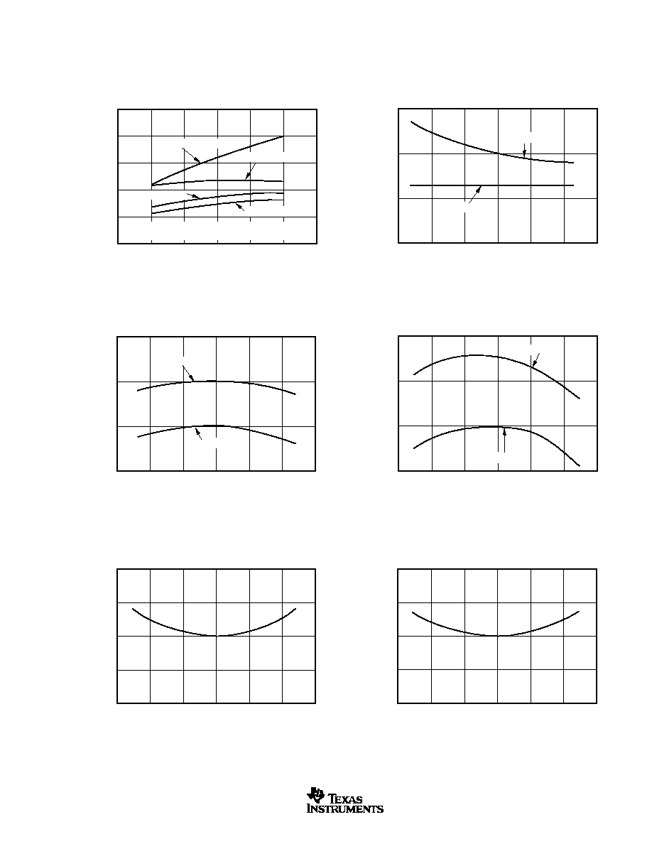
SPECTRAL PERFORMANCE
Frequency (MHz)
Amplitude (dB)
0
5
10
15
20
0
�20
�40
�60
�80
�100
�120
f
IN
= 500kHz
SPECTRAL PERFORMANCE
Frequency (MHz)
Amplitude (dB)
0
5
10
15
20
0
�20
�40
�60
�80
�100
�120
f
IN
= 5MHz
SPECTRAL PERFORMANCE
Frequency (MHz)
Amplitude (dB)
0
5
10
15
20
0
�20
�40
�60
�80
�100
�120
f
IN
= 12MHz
SPECTRAL PERFORMANCE
Frequency (MHz)
Amplitude (dB)
0
1.0
2.0
3.0
4.0
5.0
0
�20
�40
�60
�80
�100
�120
f
IN
= 1MHz
f
S
= 10MHz
DIFFERENTIAL LINEARITY ERROR
Code
DLE (LSB)
2.0
1.0
0
�1.0
�2.0
Code
0
256
512
768
1024
f
IN
= 500kHz
DIFFERENTIAL LINEARITY ERROR
Code
DLE (LSB)
2.0
1.0
0
�1.0
�2.0
Code
0
256
512
768
1024
f
IN
= 12MHz

www.ti.com
ADS821
6
SBAS040B
TYPICAL CHARACTERISTICS
(Cont.)
At T
A
= +25
�
C, V
S
= +5V, Sampling Rate = 40MHz, and with a 50% duty cycle clock having a 2ns rise-and-fall time, unless otherwise noted.
0
�20
�40
�60
�80
�100
�120
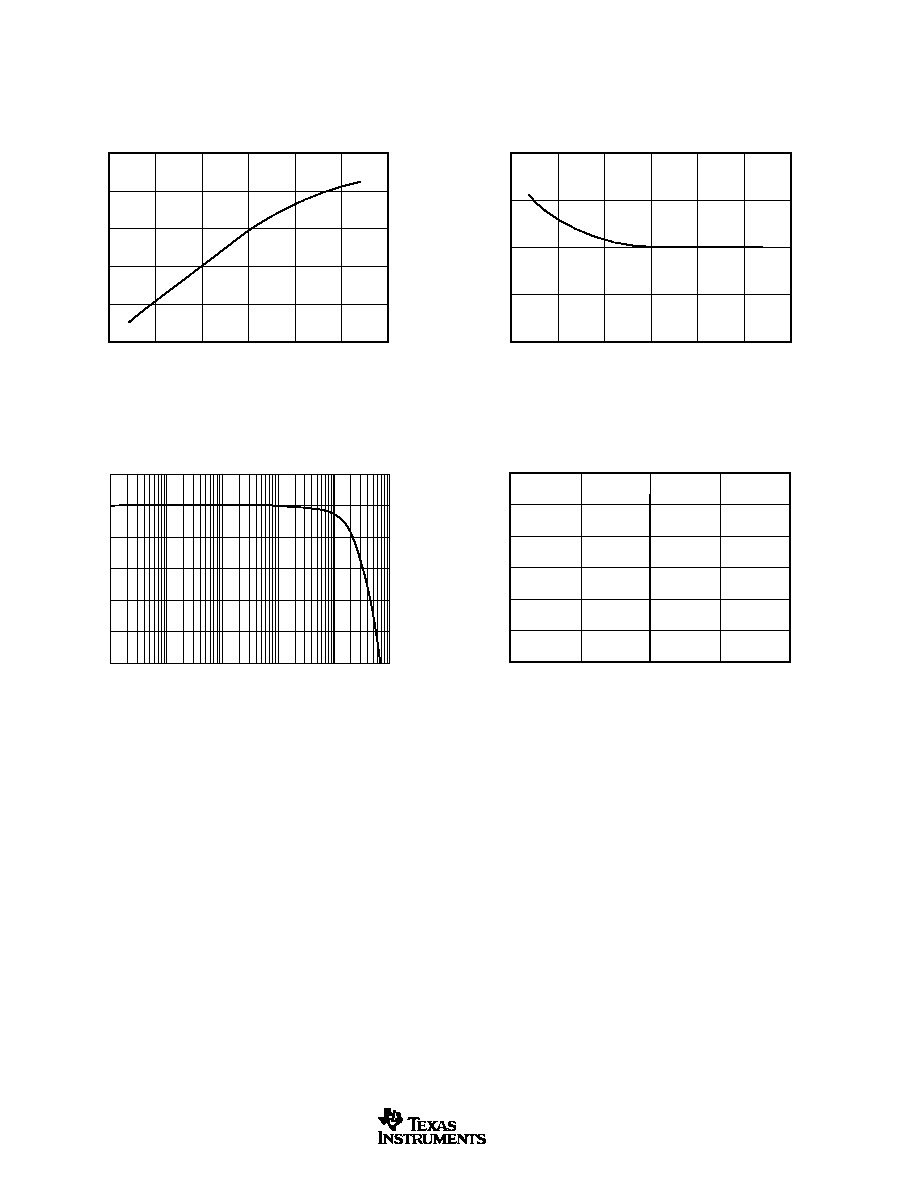
2-TONE INTERMODULATION
Amplitude (dB)
0.0
5.00
10.00
15.00
20.00
Frequency (MHz)
f
1
= 4.47MHz
f
2
= 4.39MHz
DYNAMIC PERFORMANCE vs INPUT FREQUENCY
Frequency (MHz)
SFDR, SNR (dB)
70
65
60
55
0.1
1
10
100
SFDR
SNR
100
80
60
40
20
0
Input Amplitude (dBm)
SFDR (dBFS)
SWEPT POWER SFDR
�50
�40
�30
�20
�10
0
10
f
IN
= 12MHz
60
50
40
30
20
10
0
Input Amplitude (dBm)
SWEPT POWER SNR
�50
�40
�30
�20
�10
0
10
SNR (dB)
f
IN
= 12MHz
4.0
2.0
0
�2.0
�4.0
INTEGRAL LINEARITY ERROR
Code
ILE (LSB)
f
IN
= 500kHz
0.0
0.20
0.40
0.60
0.80
1.0
65
60
55
50
45
40
DYNAMIC PERFORMANCE vs
SINGLE-ENDED FULL-SCALE INPUT RANGE
Dynamic Range (dB)
2
3
4
Single-Ended Full-Scale Input Range (Vp-p)
SNR (f
IN
= 12MHz)
SFDR (f
IN
= 500kHz)
SNR (f
IN
= 500kHz)
SFDR (f
IN
= 12MHz)
NOTE: REFT
EXT
varied, REFB is fixed at the internal
value of +1.25V.
www.ti.com
ADS821
7
SBAS040B
TYPICAL CHARACTERISTICS
(Cont.)
At T
A
= +25
�
C, V
S
= +5V, Sampling Rate = 40MHz, and with a 50% duty cycle clock having a 2ns rise-and-fall time, unless otherwise noted.
SPURIOUS-FREE DYNAMIC RANGE vs
TEMPERATURE
Temperature (
�
C)
SFDR (dBFS)
80
70
60
50
�50
�25
0
25
50
75
100
f
IN
= 500kHz
f
IN
= 12MHz
SIGNAL-TO-NOISE RATIO vs TEMPERATURE
Temperature (
�
C)
SNR (dB)
60
59
58
57
�50
�25
0
25
50
75
100
f
IN
= 500kHz
f
IN
= 12MHz
SIGNAL-TO-(NOISE + DISTORTION) vs TEMPERATURE
Temperature (
�
C)
SINAD (dB)
59
58
57
56
�50
�25
0
25
50
75
100
f
IN
= 500kHz
f
IN
= 10MHz
SUPPLY CURRENT vs TEMPERATURE
Temperature (
�
C)
I
Q
(mA)
67
66
65
�50
�25
0
25
50
75
100
POWER DISSIPATION vs TEMPERATURE
Temperature (
�
C)
Power (mW)
335
330
325
�50
�25
0
25
50
75
100
75
70
65
60
55
70
DYNAMIC PERFORMANCE vs
DIFFERENTIAL FULL-SCALE INPUT RANGE
Dynamic Range (dB)
2
3
4
Differential Full-Scale Input Range (Vp-p)
SNR (f
IN
= 500kHz)
SNR (f
IN
= 12MHz)
SFDR (f
IN
= 12MHz)
SFDR (f
IN
= 500kHz)
NOTE: REFT
EXT
varied, REFB is fixed at internal
value of +1.25V.
www.ti.com
ADS821
8
SBAS040B
TYPICAL CHARACTERISTICS
(Cont.)
At T
A
= +25
�
C, V
S
= +5V, Sampling Rate = 40MHz, and with a 50% duty cycle clock having a 2ns rise-and-fall time, unless otherwise noted.
GAIN ERROR vs TEMPERATURE
Temperature (
�
C)
Gain (% FSR)
0
�0.25
�0.5
�0.75
�1.0
�1.25
�50
�25
0
25
50
75
100
OFFSET ERROR vs TEMPERATURE
Temperature (
�
C)
Offset (% FSR)
�1.75
�2.0
�2.25
�50
�25
0
25
50
75
100
TRACK-MODE SMALL-SIGNAL INPUT BANDWIDTH
Frequency (Hz)
Track-Mode Input Response (dB)
10k
1
0
�1
�2
�3
�4
�5
100k
1M
10M
100M
1G
OUTPUT NOISE HISTOGRAM (NO SIGNAL)
Counts
1.2M
1M
0.8M
0.6M
0.4M
0.2M
0.0
Code
N � 2
N � 1
N
N + 1
N + 2

www.ti.com
ADS821
9
SBAS040B
FIGURE 1. Input Track-and-Hold Configuration with Timing
Signals.
FIGURE 2. Pipeline A/D Converter Architecture.
THEORY OF OPERATION
The ADS821 is a high-speed, sampling A/D converter with
pipelining. It uses a fully differential architecture and digital
error correction to ensure 10-bit resolution. The differential
track-and-hold circuit is shown in Figure 1. The switches are
controlled by an internal clock that has a non-overlapping 2-
phase signal,
1 and
2. At the sampling time, the input
signal is sampled on the bottom plates of the input capaci-
tors. In the next clock phase,
2, the bottom plates of the
input capacitors are connected together and the feedback
capacitors are switched to the op amp output. At this time,
the charge redistributes between C
I
and C
H
, completing one
track-and-hold cycle. The differential output is a held DC
representation of the analog input at the sample time. The
track-and-hold circuit can also convert a single-ended input
signal into a fully differential signal for the quantizer.
The pipelined quantizer architecture has 9 stages with each
stage containing a 2-bit quantizer and a 2-bit Digital-to-
Analog Converter (DAC), as shown in Figure 2. Each 2-bit
quantizer stage converts on the edge of the sub-clock, which
is twice the frequency of the externally applied clock. The
output of each quantizer is fed into its own delay line to
1
1
2
1
1
1
1
1
2
1
2
1
2
IN
IN
OUT
OUT
Op Amp
Bias
V
CM
Op Amp
Bias
V
CM
C
H
C
I
C
I
C
H
Input Clock (50%)
Internal Non-Overlapping Clock
B1 (MSB)
B2
B3
B4
B5
B6
B7
B8
B9
B10 (LSB)
2-Bit
DAC
2-Bit
Flash
Input
T&H
Digital Delay
x2
x2
2-Bit
DAC
2-Bit
Flash
Digital Delay
2-Bit
Flash
Digital Delay
2-Bit
DAC
2-Bit
Flash
Digital Delay
x2
Digital Error Correction
IN
IN
Stage 1
Stage 2
Stage 8
Stage 9
+
�
+
�
+
�

www.ti.com
ADS821
10
SBAS040B
time-align it with the data created from the following quan-
tizer stages. This aligned data is fed into a digital error
correction circuit that can adjust the output data based on the
information found on the redundant bits. This technique gives
the ADS821 excellent differential linearity and ensures no
missing-codes at the 10-bit level.
The output data is available in Straight Offset Binary (SOB) or
Binary Two's Complement (BTC) format.
THE ANALOG INPUT AND INTERNAL REFERENCE
The analog input of the ADS821 can be configured in various
ways and driven with different circuits, depending on the
nature of the signal and the level of performance desired. The
ADS821 has an internal reference that sets the full-scale
input range of the A/D converter. The differential input range
has each input centered around the common-mode of +2.25V,
with each of the two inputs having a full-scale range of +1.25V
to +3.25V. Since each input is 2Vp-p and 180
�
out-of-phase
with the other, a 4V differential input signal to the quantizer
results. As shown in Figure 3, the positive full-scale reference
(REFT) and the negative full-scale reference (REFB) are
brought out for external bypassing. In addition, the common-
mode (CM) voltage may be used as a reference to provide the
appropriate offset for the driving circuitry. However, care must
be taken not to appreciably load this reference node. For
more information regarding external references, single-ended
inputs, and ADS821 drive circuits, refer to the applications
section.
�
For most applications, the clock duty should be set to
50%. For applications requiring no missing codes, how-
ever, a slight skew in the duty cycle will improve DNL
performance for conversion rates > 35MHz and input
frequencies < 2MHz (see Timing Diagram) in the SO
package. For the best performance in the SSOP pack-
age, the clock should be skewed under all input frequen-
cies with conversion rates > 35MHz. A possible method
for skewing the 50% duty cycle source is shown in Figure 4.
FIGURE 3. Internal Reference Structure.
CLOCK REQUIREMENTS
The CLK pin accepts a CMOS level clock input. Both the
rising and falling edges of the externally applied clock con-
trols the various interstage conversions in the pipeline. There-
fore, the clock signal's jitter, rise-and-fall times and duty cycle
can affect conversion performance.
�
Low clock jitter is critical to SNR performance in fre-
quency-domain signal environments.
�
Clock rise and fall times should be as short as possible
(< 2ns for best performance).
FIGURE 4. Clock Skew Circuit.
DIGITAL OUTPUT DATA
The 10-bit output data is provided at CMOS logic levels. There
is a 6.5 clock cycle data latency from the start convert signal
to the valid output data. The standard output coding is Straight
Offset Binary where a full-scale input signal corresponds to all
"1's" at the output. This condition is met with pin 19 LOW or
Floating due to an internal pull-down resistor. By applying a
high voltage to this pin, a BTC output will be provided where
the most significant bit is inverted. The digital outputs of the
ADS821 can be set to a high impedance state by driving OE
(pin 18) with a logic HIGH. Normal operation is achieved with
pin 18 LOW or Floating due to internal pull-down resistors. This
function is provided for testability purposes and is not meant to
drive digital buses directly or be dynamically changed during
the conversion process.
OUTPUT CODE
SOB
BTC
PIN 19
PIN 19
DIFFERENTIAL INPUT
(1)
FLOATING or LOW
HIGH
+FS (IN = +3.25V, IN = +1.25V)
1111111111
0111111111
+FS � 1LSB
1111111111
0111111111
+FS � 2LSB
1111111110
0111111110
+3/4 Full-Scale
1110000000
0110000000
+1/2 Full-Scale
1100000000
0100000000
+1/4 Full-Scale
1010000000
0010000000
+1LSB
1000000001
0000000001
Bipolar Zero (IN = IN = +2.25V)
1000000000
0000000000
�1LSB
0111111111
1111111111
�1/4 Full-Scale
0110000000
1110000000
�1/2 Full-Scale
0100000000
1100000000
�3/4 Full-Scale
0010000000
1010000000
�FS + 1LSB
0000000001
1000000001
�FS (IN = +1.25V, IN = +3.25V)
0000000000
1000000000
NOTE: (1) In the single-ended input mode, +FS = +4.25V and �FS = +0.25V.
TABLE I. Coding Table for the ADS821.
+1.25V
+3.25V
2k
2k
0.1
�
F
0.1
�
F
+2.25V
REFT
REFB
CM
ADS821
To
Internal
Comparators
21
22
23
0.1
�
F
R
V
2k
V
DD
0.1
�
F
V
DD
CLK
OUT
CLK
IN
IC2
IC1
IC1, IC2 = ACT04
R
V
= 217
, Typical
www.ti.com
ADS821
11
SBAS040B
APPLICATIONS
DRIVING THE ADS821
The ADS821 has a differential input with a common-mode of
+2.25V. For AC-coupled applications, the simplest way to
create this differential input is to drive the primary winding of
a transformer with a single-ended input. A differential output
is created on the secondary if the center tap is tied to the
common-mode (CM) voltage of +2.25V, as per Figure 5. This
transformer-coupled input arrangement provides good high-
frequency AC performance. It is important to select a trans-
former that gives low distortion and does not exhibit core
saturation at full-scale voltage levels. Since the transformer
does not appreciably load the ladder, there is no need to
buffer the CM output in this instance. In general, it is
advisable to keep the current draw from the CM output pin
below 0.5
�
A to avoid nonlinearity in the internal reference
ladder. A FET input operational amplifier such as the OPA130
can provide a buffered reference for driving external circuitry.
The analog IN and IN inputs should be bypassed with 22pF
capacitors to minimize track-and-hold glitches and to im-
prove high-input frequency performance.
Figure 6 shows an AC-coupled single-ended input interface
circuit using the low-cost, current feedback OPA694 as the
active gain stage. When testing this configuration in gains of
+4, +5.8, and +8.2, it was noted that reducing the feedback
resistor of the OPA694 from the typical 402
to 360
resulted in a wider bandwidth, thus improving distortion at
higher gains. The gain resistor was scaled to 120
, 75
, and
50
for each of the three gain settings. The two 330
resistors set the RC time constant and the values can be
varied, although higher values will have the effect of moving
the corner frequency of the created high-pass filter down. In
Figure 6, the �3dB point is set at 4.2kHz.
Figure 7 illustrates another possible low-cost interface circuit
that utilizes resistors and capacitors in place of a transformer.
Depending on the signal bandwidth, the component values
should be carefully selected in order to maintain the perfor-
mance outlined in the data sheet. The input capacitors, C
IN
,
and the input resistors, R
IN
, create a high-pass filter with the
lower corner frequency at f
C
= 1/(2
R
IN
C
IN
). The corner
frequency can be reduced by either increasing the value of
R
IN
or C
IN
. If the circuit operates with a 50
or 75
imped-
ance level, the resistors are fixed and only the value of the
capacitor can be increased. Usually AC-coupling capacitors
are electrolytic or tantalum capacitors with values of 1mF or
higher. It should be noted that these large capacitors become
inductive with increased input frequency, which could lead to
signal amplitude errors or oscillation. To maintain a low AC-
coupling impedance throughout the signal band, a small
value (e.g. 1
�
F) ceramic capacitor could be added in parallel
with the polarized capacitor.
Capacitors C
SH1
and C
SH2
are used to minimize current
glitches resulting from the switching in the input track-and-
hold stage and to improve signal-to-noise performance. These
capacitors can also be used to establish a low-pass filter and
effectively reduce the noise bandwidth. In order to create a
real pole, resistors R
SER1
and R
SER2
were added in series with
each input. The cut off frequency of the filter is determined by
f
C
= 1/(2
R
SER
� (C
SH
+ C
ADC
)) where R
SER
is the resistor in
series with the input, C
SH
is the external capacitor from the
input to ground, and C
ADC
is the internal input capacitance of
the A/D converter (typically 4pF).
Resistors R
1
and R
2
are used to derive the necessary com-
mon-mode voltage from the buffered top and bottom refer-
ences.
The total load of the resistor string should be selected
FIGURE 5. AC-Coupled, Single-Ended to Differential Drive
Circuit Using a Transformer.
FIGURE 6. Low-Cost, AC-Coupled, Single-Ended Input Circuit.
Mini-Circuits
T T1-6-KK81
or Equivalent
22
26
27
CM
IN
IN
ADS821
AC Input
Signal
22pF
22pF
0.1
�
F
ADS821
A
1
V
IN
R
G
OPA694
0.1 || 2.2
0.1 || 2.2
+5V
�5V
I/O
360
330
330
IN
27
26
22
CM
+2.25V
IN
22pF
49.9
0.1
�
F
0.1
�
F
0.1
�
F

www.ti.com
ADS821
12
SBAS040B
so that the current does not exceed 1mA. Although the circuit
in Figure 7 uses two resistors of equal value so that the
common-mode voltage is centered between the top and bot-
tom reference (+2.25V), it is not necessary to do so. In all
cases the center point, V
CM
, should be bypassed to ground in
order to provide a low-impedance AC ground.
If the signal needs to be DC-coupled to the input of the
ADS821, an operational amplifier input circuit is required. In
the differential input mode, any single-ended signal must be
modified to create a differential signal. This can be accom-
plished by using two operational amplifiers, one in the
noninverting mode for the input and the other amplifier in the
inverting mode for the complementary input. The low-distor-
tion circuit in Figure 8 will provide the necessary input shifting
required for signals centered around ground. It also employs
a diode for output level shifting to ensure a low-distortion
+3.25V output swing. See Figure 9 for another DC-coupled
circuit. Other amplifiers can be used in place of the OPA860
if the lowest distortion is not necessary. If output level shifting
circuits are not used, care must be taken to select opera-
tional amplifiers that give the necessary performance when
swinging to +3.25V with a
�
5V supply operational amplifier.
The OPA620 and OPA621, or the lower power OPA650 or
OPA820 can be used in place of the OPA860 in Figure 8. In
that configuration, the OPA820 will typically swing to within
100mV of positive full scale.
The ADS821 can also be configured with a single-ended input
full-scale range of +0.25V to +4.25V by tying the complemen-
tary input to the common-mode reference voltage, see Figure 10.
This configuration will result in increased even-order harmon-
ics, especially at higher input frequencies. This tradeoff,
however, may be quite acceptable for time-domain applica-
tions. The driving amplifier must give adequate performance
with a +0.25V to +4.25V output swing in this case.
EXTERNAL REFERENCES AND ADJUSTMENT OF
FULL-SCALE RANGE
The internal-reference buffers are limited to approximately
1mA of output current. As a result, these internal +1.25V and
+3.25V references may be overridden by external references
that have at least 18mA (at room temperature) of output drive
capability. In this instance, the common-mode voltage will be
set halfway between the two references. This feature can be
used to adjust the gain error, improve gain drift, or to change
the full-scale input range of the ADS821. Changing the full-
scale range to a lower value has the benefit of easing the
swing requirements of external input amplifiers. The external
references can vary as long as the value of the external top
reference (REFT
EXT
) is less than or equal to +3.4V, the value
of the external bottom reference (REFB
EXT
) is greater than or
equal to +1.1V, and the difference between the external
references are greater than or equal to 800mV.
For the differential configuration, the full-scale input range
will be set to the external reference values that are
selected. For the single-ended mode, the input range is
2 � (REFT
EXT
� REFB
EXT
), with the common-mode being
centered at (REFT
EXT
+ REFB
EXT
)/2. Refer to the Typical
Characteristics for expected performance versus full-scale
input range.
The circuit in Figure 11 works completely on a single +5V
supply. As a reference element, it uses the
microPower
reference REF1004-2.5, which is set to a quiescent current
of 0.1mA. Amplifier A
2
is configured as a follower to buffer the
+1.25V generated from the resistor divider. To provide the
necessary current drive, a pull-down resistor (R
P
) is added.
Amplifier A
1
is configured as an adjustable gain stage, with
a range of approximately 1 to 1.32. The pull-up resistor again
relieves the op amp from providing the full current drive. The
value of the pull-up, pull-down resistors is not critical and can
be varied to optimize power consumption. The need for pull-
up, pull-down resistors depends only on the drive capability
of the selected drive amplifier and thus can be omitted.
FIGURE 7. AC-Coupled Differential Input Circuit.
ADS8xx
R
SER1
(1)
49.9
R
3
1k
R
2
(6k
)
R
1
(6k
)
C
2
0.1
�
F
C
SH1
22pF
C
SH2
22pF
C
3
0.1
�
F
C
1
0.1
�
F
C
IN
0.1
�
F
V
CM
C
IN
0.1
�
F
R
IN1
25
R
IN2
25
R
SER2
(1)
49.9
+3.25V
Top Reference
+1.25V
Bottom Reference
IN
NOTE: (1) indicates optional component.
IN
www.ti.com
ADS821
13
SBAS040B
FIGURE 9. A Wideband DC-Coupled, Single-Ended to Differential Input Driver Circuit.
FIGURE 8. A Low-Distortion DC-Coupled, Single-Ended to Differential Input Driver Circuit.
604
301
301
301
604
49.9
301
604
2.49k
2.49k
+2.25V
OPA842
OPA130
301
0.1
�
F
OPA842
OPA842
+5V
�5V
+5V
(2)
+5V
�5V
+5V
+5V
+5V
�5V
BAS16
(1)
BAS16
(1)
301
24.9
Input Level
Shift Buffer
Optional
High Impedance
Input Amplifier
DC-Coupled
Input Signal
26 IN
22 CM
27 IN
ADS821
NOTES: (1) A Philips BAS16 diode or equivalent may be used.
(2) Supply bypassing not shown.
22pF
22pF
604
0.1
�
F
0.1
�
F
50
1k
OTA
OPA860
OPA860
+1
+1
OPA130
1nF
OTA
�5V
+5V
DC-Coupled
Input Signal
27 IN
22 CM
26 IN
ADS821
NOTE: Power supplies and bypassing not shown. The measured SNR performance with 12.5MHz input signal is 57dB with this driver circuit.
1k
500
500
1k
200
243
200
3
B
2
3
2
8
5
C
6
1
6
1
8
5
C
E
E
3
2
B
200
C
1
15pF
22pF
22pF
0.1
�
F
2k
V
OUT
V
OUT
�5V
243

www.ti.com
ADS821
14
SBAS040B
results. Highly accurate phase-locked signal sources allow
high resolution FFT measurements to be made without using
data windowing functions. A low jitter signal generator, such as
the HP8644A for the test signal, phase-locked with a low jitter
HP8022A pulse generator for the A/D converter clock, gives
excellent results. Low-pass filtering (or bandpass filtering) of
test signals is absolutely necessary to test the low distortion of
the ADS821. Using a signal amplitude slightly lower than full
scale will allow a small amount of "headroom" so that noise or
DC offset voltage will not overrange the A/D converter and
cause clipping on signal peaks.
DYNAMIC PERFORMANCE DEFINITIONS
1. Signal-to-Noise-and-Distortion Ratio (SINAD):
10
15
log
(
)
Sinewave Signal Power
Noise
Harmonic Power first
harmonics
+
2. Signal-to-Noise Ratio (SNR):
10 log
Sinewave Signal Power
Noise Power
3. Intermodulation Distortion (IMD):
10
5
log
Pr
(
)
Highest IMD
oduct Power to th order
Sinewave Signal Power
-
IMD is referenced to the larger of the test signals f
1
or f
2
. Five
"bins" either side of peak are used for calculation of funda-
mental and harmonic power. The "0" frequency bin (DC) is
not included in these calculations as it is of little importance
in dynamic signal processing applications.
FIGURE 10. Single-Ended Input Connection.
PC-BOARD LAYOUT AND BYPASSING
A well-designed, clean PC-board layout will assure proper
operation and clean spectral response. Proper grounding
and bypassing, short lead lengths, and the use of ground
planes are particularly important for high-frequency circuits.
Multilayer PC-boards are recommended for best perfor-
mance but if carefully designed, a two-sided PC-board with
large, heavy ground planes can give excellent results. It is
recommended that the analog and digital ground pins of the
ADS821 be connected directly to the analog ground plane. In
our experience, this gives the most consistent results. The
A/D converter power-supply commons should be tied to-
gether at the analog ground plane. Power supplies should be
bypassed with 0.1
�
F ceramic capacitors as close to the pin
as possible.
DYNAMIC PERFORMANCE TESTING
The ADS821 is a high-performance converter and careful
attention to test techniques is necessary to achieve accurate
FIGURE 11. Optional External Reference to Set the Full-Scale Range Utilizing a Dual, Single-Supply Op Amp.
22
26
27
CM
IN
IN
ADS821
0.1
�
F
Single-Ended
Input Signal
Full-Scale = +0.25V to +4.25V with internal references.
22pF
2k
+2.5V to +3.25V
+5V
+5V
R
P
220
R
P
220
10k
6.2k
0.1
�
F
+2.5V
10k
1/2
OPA2234
1/2
OPA2234
A
1
A
2
Bottom
Reference
Top
Reference
REF1004
+1.25V
10k
10k
(1)
10k
(1)
NOTE: (1) Use parts alternatively for adjustment capability.

www.ti.com
ADS821
15
SBAS040B
FIGURE 12. ADS821 Interface Schematic with AC-Coupling and External Buffers.
GND
DNC
DNC
LSB
MSB
GND
11
12
13
14
15
16
17
18
9
8
7
6
5
4
3
2
1
19
+V
S
CLK
+V
S
OE
MSBI
+V
S
REFB
CM
REFT
+V
S
GND
IN
IN
GND
15
16
17
18
19
20
21
22
23
24
25
26
27
28
14
13
12
11
10
9
8
7
6
5
4
3
2
1
ADS821
0.1
�
F
0.1
�
F
0.1
�
F
0.1
�
F
0.1
�
F
0.1
�
F
0.1
�
F
R
1
50
R
2
50
Ext
Clk
AC Input
Signal
11
12
13
14
15
16
17
18
9
8
7
6
5
4
3
2
Dir
G+
1
19
Dir
G+
�
541
�
541
Mini-Circuits
T
T1-6-KK81
or equivalent
22pF
22pF
(1)
NOTE: (1) All capacitors should be located as close to the pins as the manufacturing
process will allow. Ceramic X7R surface-mount capacitors or equivalent are recommended.
+5V

PACKAGING INFORMATION
Orderable Device
Status
(1)
Package
Type
Package
Drawing
Pins Package
Qty
Eco Plan
(2)
Lead/Ball Finish
MSL Peak Temp
(3)
ADS821E
OBSOLETE
SSOP
DB
28
None
Call TI
Call TI
ADS821E/1K
OBSOLETE
SSOP
DB
28
None
Call TI
Call TI
ADS821U
ACTIVE
SOIC
DW
28
28
None
CU SNPB
Level-3-220C-168 HR
(1)
The marketing status values are defined as follows:
ACTIVE: Product device recommended for new designs.
LIFEBUY: TI has announced that the device will be discontinued, and a lifetime-buy period is in effect.
NRND: Not recommended for new designs. Device is in production to support existing customers, but TI does not recommend using this part in
a new design.
PREVIEW: Device has been announced but is not in production. Samples may or may not be available.
OBSOLETE: TI has discontinued the production of the device.
(2)
Eco Plan - May not be currently available - please check
http://www.ti.com/productcontent
for the latest availability information and additional
product content details.
None: Not yet available Lead (Pb-Free).
Pb-Free (RoHS): TI's terms "Lead-Free" or "Pb-Free" mean semiconductor products that are compatible with the current RoHS requirements
for all 6 substances, including the requirement that lead not exceed 0.1% by weight in homogeneous materials. Where designed to be soldered
at high temperatures, TI Pb-Free products are suitable for use in specified lead-free processes.
Green (RoHS & no Sb/Br): TI defines "Green" to mean "Pb-Free" and in addition, uses package materials that do not contain halogens,
including bromine (Br) or antimony (Sb) above 0.1% of total product weight.
(3)
MSL, Peak Temp. -- The Moisture Sensitivity Level rating according to the JEDECindustry standard classifications, and peak solder
temperature.
Important Information and Disclaimer:The information provided on this page represents TI's knowledge and belief as of the date that it is
provided. TI bases its knowledge and belief on information provided by third parties, and makes no representation or warranty as to the
accuracy of such information. Efforts are underway to better integrate information from third parties. TI has taken and continues to take
reasonable steps to provide representative and accurate information but may not have conducted destructive testing or chemical analysis on
incoming materials and chemicals. TI and TI suppliers consider certain information to be proprietary, and thus CAS numbers and other limited
information may not be available for release.
In no event shall TI's liability arising out of such information exceed the total purchase price of the TI part(s) at issue in this document sold by TI
to Customer on an annual basis.
PACKAGE OPTION ADDENDUM
www.ti.com
14-Feb-2005
Addendum-Page 1


IMPORTANT NOTICE
Texas Instruments Incorporated and its subsidiaries (TI) reserve the right to make corrections, modifications,
enhancements, improvements, and other changes to its products and services at any time and to discontinue
any product or service without notice. Customers should obtain the latest relevant information before placing
orders and should verify that such information is current and complete. All products are sold subject to TI's terms
and conditions of sale supplied at the time of order acknowledgment.
TI warrants performance of its hardware products to the specifications applicable at the time of sale in
accordance with TI's standard warranty. Testing and other quality control techniques are used to the extent TI
deems necessary to support this warranty. Except where mandated by government requirements, testing of all
parameters of each product is not necessarily performed.
TI assumes no liability for applications assistance or customer product design. Customers are responsible for
their products and applications using TI components. To minimize the risks associated with customer products
and applications, customers should provide adequate design and operating safeguards.
TI does not warrant or represent that any license, either express or implied, is granted under any TI patent right,
copyright, mask work right, or other TI intellectual property right relating to any combination, machine, or process
in which TI products or services are used. Information published by TI regarding third-party products or services
does not constitute a license from TI to use such products or services or a warranty or endorsement thereof.
Use of such information may require a license from a third party under the patents or other intellectual property
of the third party, or a license from TI under the patents or other intellectual property of TI.
Reproduction of information in TI data books or data sheets is permissible only if reproduction is without
alteration and is accompanied by all associated warranties, conditions, limitations, and notices. Reproduction
of this information with alteration is an unfair and deceptive business practice. TI is not responsible or liable for
such altered documentation.
Resale of TI products or services with statements different from or beyond the parameters stated by TI for that
product or service voids all express and any implied warranties for the associated TI product or service and
is an unfair and deceptive business practice. TI is not responsible or liable for any such statements.
Following are URLs where you can obtain information on other Texas Instruments products and application
solutions:
Products
Applications
Amplifiers
amplifier.ti.com
Audio
www.ti.com/audio
Data Converters
dataconverter.ti.com
Automotive
www.ti.com/automotive
DSP
dsp.ti.com
Broadband
www.ti.com/broadband
Interface
interface.ti.com
Digital Control
www.ti.com/digitalcontrol
Logic
logic.ti.com
Military
www.ti.com/military
Power Mgmt
power.ti.com
Optical Networking
www.ti.com/opticalnetwork
Microcontrollers
microcontroller.ti.com
Security
www.ti.com/security
Telephony
www.ti.com/telephony
Video & Imaging
www.ti.com/video
Wireless
www.ti.com/wireless
Mailing Address:
Texas Instruments
Post Office Box 655303 Dallas, Texas 75265
Copyright
2005, Texas Instruments Incorporated